EP0309714A2 - Récepteur à onde de surface à multiplication de fréquence et à amplification - Google Patents
Récepteur à onde de surface à multiplication de fréquence et à amplification Download PDFInfo
- Publication number
- EP0309714A2 EP0309714A2 EP88113281A EP88113281A EP0309714A2 EP 0309714 A2 EP0309714 A2 EP 0309714A2 EP 88113281 A EP88113281 A EP 88113281A EP 88113281 A EP88113281 A EP 88113281A EP 0309714 A2 EP0309714 A2 EP 0309714A2
- Authority
- EP
- European Patent Office
- Prior art keywords
- surface wave
- wave receiver
- voltage source
- contact electrodes
- frequency
- Prior art date
- Legal status (The legal status is an assumption and is not a legal conclusion. Google has not performed a legal analysis and makes no representation as to the accuracy of the status listed.)
- Withdrawn
Links
- 239000000463 material Substances 0.000 claims abstract description 11
- 239000000758 substrate Substances 0.000 claims abstract description 9
- 230000000694 effects Effects 0.000 claims abstract description 8
- 229910001218 Gallium arsenide Inorganic materials 0.000 claims description 4
- 239000007769 metal material Substances 0.000 claims description 2
- 239000004065 semiconductor Substances 0.000 claims description 2
- 230000003014 reinforcing effect Effects 0.000 abstract 1
- 238000010897 surface acoustic wave method Methods 0.000 description 3
- 238000001514 detection method Methods 0.000 description 2
- XAGFODPZIPBFFR-UHFFFAOYSA-N aluminium Chemical compound [Al] XAGFODPZIPBFFR-UHFFFAOYSA-N 0.000 description 1
- 229910052782 aluminium Inorganic materials 0.000 description 1
- 230000003321 amplification Effects 0.000 description 1
- 238000011161 development Methods 0.000 description 1
- 230000018109 developmental process Effects 0.000 description 1
- 238000010586 diagram Methods 0.000 description 1
- 230000005284 excitation Effects 0.000 description 1
- 239000011810 insulating material Substances 0.000 description 1
- 230000010354 integration Effects 0.000 description 1
- 238000012986 modification Methods 0.000 description 1
- 230000004048 modification Effects 0.000 description 1
- 238000003199 nucleic acid amplification method Methods 0.000 description 1
- 230000002787 reinforcement Effects 0.000 description 1
- 230000001629 suppression Effects 0.000 description 1
Images
Classifications
-
- H—ELECTRICITY
- H03—ELECTRONIC CIRCUITRY
- H03B—GENERATION OF OSCILLATIONS, DIRECTLY OR BY FREQUENCY-CHANGING, BY CIRCUITS EMPLOYING ACTIVE ELEMENTS WHICH OPERATE IN A NON-SWITCHING MANNER; GENERATION OF NOISE BY SUCH CIRCUITS
- H03B19/00—Generation of oscillations by non-regenerative frequency multiplication or division of a signal from a separate source
-
- H—ELECTRICITY
- H03—ELECTRONIC CIRCUITRY
- H03B—GENERATION OF OSCILLATIONS, DIRECTLY OR BY FREQUENCY-CHANGING, BY CIRCUITS EMPLOYING ACTIVE ELEMENTS WHICH OPERATE IN A NON-SWITCHING MANNER; GENERATION OF NOISE BY SUCH CIRCUITS
- H03B2200/00—Indexing scheme relating to details of oscillators covered by H03B
- H03B2200/0014—Structural aspects of oscillators
- H03B2200/0022—Structural aspects of oscillators characterised by the substrate, e.g. material
Definitions
- the present invention relates to a frequency-doubling, amplifying surface wave receiver for a surface wave element made of a material which can be made electrically conductive by the piezo effect and by local doping.
- transducer structures In the case of surface acoustic wave components, the signals passing through the component are coupled out via transducer structures. These transducer structures generally consist of metallic tracks that are arranged on an insulating substrate. The surface wave couples charges into the body of the surface wave component via the piezo effect, which can be tapped as a signal. However, the energy content of these signals is relatively small, so that the signal in question has to be amplified after it has been decoupled and adapted to corresponding further processing electronic components.
- the detection of surface wave components requires the detection of both the fundamental wave with the frequency f and the harmonic wave with the frequency 2f.
- the production of components that have an active suppression or enhancement of harmonics requires the monolithic integration of frequency-doubling components.
- the control of further converter structures requires high signal levels.
- the object of the present invention is to create a frequency-doubling, amplifying receiver for surface waves, with the aid of which a harmonic with the frequency 2f of a fundamental wave with the frequency f is recognized in a particularly simple manner and a necessary amplification of the signal passing through the surface wave component is achieved can be.
- the object on which the present invention is based is achieved by a frequency-doubling, amplifying surface wave receiver of the type mentioned at the outset and according to the preamble of patent claim 1, which according to the invention is characterized by the features specified in the characterizing part of claim 1.
- Known piezoelectric transducers consist of a substrate body made of an insulating material that shows the piezo effect. Two metallic contact electrodes are applied to the surface of this substrate body at a predetermined distance, each of which is connected to a terminal of an AC voltage detector.
- the operation of such an arrangement is described, for example, in IEEE 1982 ULTRA SONICS SYMPOSIUM, pages 456 to 460, Michael J. Hoskins and Bill J. Hunsinger: "MONOLITHIC GaAs ACOUSTIC CHARGE TRANSPORT DEVICES".
- Such a known arrangement has the disadvantage that the size of the available signal voltage at the two contact electrodes is small due to the low energy content of the signals in question, so that the signal is amplified after it is decoupled and further processed processing facilities must be adapted. Depending on the application, this may lead to difficulties, but in any case to a relatively high technical outlay. In addition, a harmonic of the fundamental vibration of the surface acoustic wave element cannot be detected.
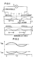
- FIG. 1 shows a schematic illustration of a preferred exemplary embodiment for the present invention.
- the illustration shows a frequency-doubling, amplifying surface wave receiver for a surface wave element made of a material that shows the piezo effect and can be made electrically conductive by local doping.
- a doping region is formed on the top of an insulating substrate body 5 which forms the surface wave element and is formed from the material characterized above, and forms a conductive channel 4 between two contact electrodes 3, 3 which are at a certain distance from one another in such a way that occurring piezo charges are able to To modulate conductivity of this channel 4.
- a pole of a voltage source 1 is connected to one of the contact electrodes 3, the other pole of which is connected to the other contact electrode 3 via an alternating current detector 2.
- the distance D between the contact electrodes 3, 3 is determined such that the condition D ⁇ ⁇ is fulfilled, the wavelength of the surface wave occurring being, which means that the distance D is so large that at least one complete wave space between the contact electrodes finds.
- the characterized material is GaAs.
- the voltage source 1 is preferably a DC voltage source, but can alternatively also be an AC voltage source, the frequency of which is in a predetermined ratio to the frequency of the surface waves.
- the contact electrodes 3, 3 preferably consist of a metallic material, for example aluminum.
- the AC detector 2 can be designed in various ways. It is preferably used as a current detector Turing semiconductor device is formed, which is applied as an integral part of the surface acoustic wave element on the substrate body 8.
- the change in the depth d of the conductive channel due to the control effect of the piezoelectric charges occurring is shown schematically in broken lines.
- This change or modulation of the conductive channel changes its resistance, so that in the circuit formed by the arrangement as a whole the current, depending on the level of the voltage of the voltage source 1, is represented as a rippled direct current or as an alternating current, said rippled direct current or alternating current in a known manner Way can be detected by the AC detector 2.
- the piezo charges act similarly to the gate charges in the case of a MESFET or MOSFET.
- the reinforcement properties depend on both the geometrical and electrical dimensions.
- the frequency doubling is achieved by the appropriate dimensioning of the electrode spacing.
- D ⁇ is assumed.
- the contact electrodes are placed in such a way that the inner edges of the contact electrodes lie on vibration nodes when the shaft is standing.
- the time profile of the current flow is shown in FIG. 2 together with the voltage profile at the electrodes that excite the shaft.
- the conductivity of the channel is not modulated compared to its equilibrium state.
- the piezo charges pinch off the part of the channel designated "1" in FIG. 1.
- Part "2" is opened at the same time. If there is such a high voltage at the contacts that the electrons reach their saturation rate in the region "1", the current flow is determined solely by the part of the channel that is cut off.
- the surface wave component according to the invention can be implemented on all substrate materials which on the one hand show the piezo effect and on the other hand can be made electrically conductive by local doping.
- a material to be used preferably, as already mentioned, is GaAs.
Landscapes
- Surface Acoustic Wave Elements And Circuit Networks Thereof (AREA)
Applications Claiming Priority (2)
| Application Number | Priority Date | Filing Date | Title |
|---|---|---|---|
| DE3732858 | 1987-09-29 | ||
| DE3732858 | 1987-09-29 |
Publications (2)
| Publication Number | Publication Date |
|---|---|
| EP0309714A2 true EP0309714A2 (fr) | 1989-04-05 |
| EP0309714A3 EP0309714A3 (fr) | 1990-08-08 |
Family
ID=6337158
Family Applications (1)
| Application Number | Title | Priority Date | Filing Date |
|---|---|---|---|
| EP88113281A Withdrawn EP0309714A3 (fr) | 1987-09-29 | 1988-08-16 | Récepteur à onde de surface à multiplication de fréquence et à amplification |
Country Status (3)
| Country | Link |
|---|---|
| US (1) | US4839607A (fr) |
| EP (1) | EP0309714A3 (fr) |
| JP (1) | JPH01115208A (fr) |
Families Citing this family (2)
| Publication number | Priority date | Publication date | Assignee | Title |
|---|---|---|---|---|
| US5001483A (en) * | 1989-10-23 | 1991-03-19 | Westinghouse Electric Corp. | Digital to analog converter for an acoustic charge transport device |
| US5435186A (en) * | 1992-10-26 | 1995-07-25 | General Electric Company | Ultrasonic parametric amplifier |
Family Cites Families (2)
| Publication number | Priority date | Publication date | Assignee | Title |
|---|---|---|---|---|
| US3713048A (en) * | 1971-07-28 | 1973-01-23 | Zenith Radio Corp | Swif{40 s with special polarization for non-linear interactions |
| US4233530A (en) * | 1978-10-05 | 1980-11-11 | Clarion Co., Ltd. | Elastic surface wave device |
-
1988
- 1988-08-16 EP EP88113281A patent/EP0309714A3/fr not_active Withdrawn
- 1988-09-16 US US07/245,371 patent/US4839607A/en not_active Expired - Fee Related
- 1988-09-28 JP JP63245828A patent/JPH01115208A/ja active Pending
Also Published As
| Publication number | Publication date |
|---|---|
| JPH01115208A (ja) | 1989-05-08 |
| EP0309714A3 (fr) | 1990-08-08 |
| US4839607A (en) | 1989-06-13 |
Similar Documents
| Publication | Publication Date | Title |
|---|---|---|
| DE3026655C2 (fr) | ||
| DE102018103166A1 (de) | Kondensator | |
| DE3204859A1 (de) | Elektrolumineszente duennfilmstruktur | |
| DE2129700A1 (de) | Anordnung zur Abstrahlung impulsfoermiger elektromagnetischer Energie | |
| DE3005179A1 (de) | Aofw-verzoegerungsleitung mit variabler verzoegerung und damit hergestellter monolithischer, spannungsgeregelter oszillator | |
| DE1276834B (de) | Elektromechanische Vorrichtung zum AEndern der Amplitude eines akustischen Signals | |
| DE202018106621U1 (de) | Kondensator | |
| DE19910889C2 (de) | Oberflächenwellenvorrichtung | |
| DE112021003299T5 (de) | Leistungshalbleitermodul und leistungsumsetzungsvorrichtung | |
| DE2713820C2 (de) | Josephson-Kontakt-Element für einen Wanderwellenverstärker | |
| DE3322310A1 (de) | Oberflaechenschallwellenvorrichtung | |
| DE2846186A1 (de) | Wechselwirkungsvorrichtung fuer magnetoelastische oberflaechenwellen | |
| EP0077481A2 (fr) | Dispositif semi-conducteur planaire | |
| EP1537610B1 (fr) | Actionneur piezo-electrique | |
| DE3049102A1 (de) | Parametrische vorrichtung zur verarbeitung von akustischen oberflaechenwellen | |
| EP0309714A2 (fr) | Récepteur à onde de surface à multiplication de fréquence et à amplification | |
| DE10050058A1 (de) | Piezoelektrischer Resonator | |
| DE1791268C2 (de) | Verzögerungsleitung für eine Lauffeldröhre mit Anschluß einer zweiten Übertragungsleitung. Ausscheidung aus: 1491448 | |
| EP0309713A2 (fr) | Récepteur amplifiant les ondes acoustiques de surface | |
| DE2209979C3 (de) | Halbleiterbauelement | |
| DE2121344A1 (de) | Wickelkondensator | |
| EP1267464B1 (fr) | Isolateur pour système de barres électriques, et assemblage d'isolation faisant usage de tels isolateurs | |
| DE2815668A1 (de) | Breitband-isolator | |
| DE112011103776B4 (de) | Piezoelektrisches Bauelement und Verfahren zu seinem Betrieb | |
| DE1439368A1 (de) | Halbleiterstromtor mit Zuendung durch Feldeffekt |
Legal Events
| Date | Code | Title | Description |
|---|---|---|---|
| PUAI | Public reference made under article 153(3) epc to a published international application that has entered the european phase |
Free format text: ORIGINAL CODE: 0009012 |
|
| AK | Designated contracting states |
Kind code of ref document: A2 Designated state(s): DE FR GB NL |
|
| PUAL | Search report despatched |
Free format text: ORIGINAL CODE: 0009013 |
|
| AK | Designated contracting states |
Kind code of ref document: A3 Designated state(s): DE FR GB NL |
|
| STAA | Information on the status of an ep patent application or granted ep patent |
Free format text: STATUS: THE APPLICATION IS DEEMED TO BE WITHDRAWN |
|
| 18D | Application deemed to be withdrawn |
Effective date: 19910301 |