EP0309713A2 - Récepteur amplifiant les ondes acoustiques de surface - Google Patents
Récepteur amplifiant les ondes acoustiques de surface Download PDFInfo
- Publication number
- EP0309713A2 EP0309713A2 EP88113280A EP88113280A EP0309713A2 EP 0309713 A2 EP0309713 A2 EP 0309713A2 EP 88113280 A EP88113280 A EP 88113280A EP 88113280 A EP88113280 A EP 88113280A EP 0309713 A2 EP0309713 A2 EP 0309713A2
- Authority
- EP
- European Patent Office
- Prior art keywords
- surface wave
- voltage source
- wave receiver
- receiver according
- amplifying
- Prior art date
- Legal status (The legal status is an assumption and is not a legal conclusion. Google has not performed a legal analysis and makes no representation as to the accuracy of the status listed.)
- Withdrawn
Links
- 239000000463 material Substances 0.000 claims abstract description 11
- 239000000758 substrate Substances 0.000 claims abstract description 10
- 230000000694 effects Effects 0.000 claims abstract description 8
- 230000003014 reinforcing effect Effects 0.000 claims abstract description 5
- 229910001218 Gallium arsenide Inorganic materials 0.000 claims description 4
- 239000007769 metal material Substances 0.000 claims description 2
- 239000004065 semiconductor Substances 0.000 claims description 2
- XAGFODPZIPBFFR-UHFFFAOYSA-N aluminium Chemical compound [Al] XAGFODPZIPBFFR-UHFFFAOYSA-N 0.000 description 1
- 229910052782 aluminium Inorganic materials 0.000 description 1
- 230000003321 amplification Effects 0.000 description 1
- 238000011161 development Methods 0.000 description 1
- 230000018109 developmental process Effects 0.000 description 1
- 239000011810 insulating material Substances 0.000 description 1
- 238000012986 modification Methods 0.000 description 1
- 230000004048 modification Effects 0.000 description 1
- 238000003199 nucleic acid amplification method Methods 0.000 description 1
- 230000002787 reinforcement Effects 0.000 description 1
- 238000010897 surface acoustic wave method Methods 0.000 description 1
Images
Classifications
-
- H—ELECTRICITY
- H03—ELECTRONIC CIRCUITRY
- H03F—AMPLIFIERS
- H03F13/00—Amplifiers using amplifying element consisting of two mechanically- or acoustically-coupled transducers, e.g. telephone-microphone amplifier
-
- H—ELECTRICITY
- H03—ELECTRONIC CIRCUITRY
- H03H—IMPEDANCE NETWORKS, e.g. RESONANT CIRCUITS; RESONATORS
- H03H9/00—Networks comprising electromechanical or electro-acoustic elements; Electromechanical resonators
- H03H9/02—Details
- H03H9/02535—Details of surface acoustic wave devices
- H03H9/0296—Surface acoustic wave [SAW] devices having both acoustic and non-acoustic properties
- H03H9/02976—Surface acoustic wave [SAW] devices having both acoustic and non-acoustic properties with semiconductor devices
Definitions
- the present invention relates to a reinforcing surface wave receiver for a surface wave element made of a material that can be made electrically conductive by the piezo effect and by local doping.
- transducer structures In the case of surface acoustic wave components, the signals passing through the component are coupled out via transducer structures. These transducer structures generally consist of metallic tracks that are arranged on an insulating substrate. The surface wave couples charges into the body of the surface wave component via the piezo effect, which can be tapped as a signal. However, the energy content of these signals is relatively small, so that the signal in question has to be amplified after it has been decoupled and adapted to corresponding further processing electronic components.
- the present invention has for its object to provide an amplifying receiver for surface waves, with the aid of which a necessary amplification of the signal passing through the surface wave component can be achieved in a particularly simple manner.
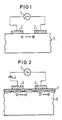
- FIG. 1 shows a piezoelectric transducer according to the prior art.
- This known piezoelectric transducer consists of a substrate body 3 made of an insulating material that shows the piezo effect. On the surface of this substrate body 3, two metallic contact electrodes 2, 2 are applied at a predetermined distance, each of which is connected to a terminal of an AC voltage detector 1.
- the operation of such an arrangement is known per se, compare for example IEEE 1982 ULTRA SONICS SYMPOSIUM, pages 456 to 460, Michael J. Hoskins and Bill J. Hunsinger: "MONOLITHIC GaAs ACOUSTIC CHARGE TRANSPORT DEVICES".
- FIG. 2 shows, as already explained, a schematic representation of a preferred embodiment for the present invention.
- the illustration shows a reinforcing surface wave receiver for a surface wave element made of a material that shows the piezo effect and can be made electrically conductive by local doping.
- a pole of a voltage source 4 is connected to one of the contact electrodes 6, the other pole of which is connected to the other contact electrode 6 via an alternating current detector 5.
- the characterized material is GaAs.
- the voltage source 4 is preferably a DC voltage source, but can alternatively also be an AC voltage source, the frequency of which is in a predetermined ratio to the frequency of the surface waves.
- the contact electrodes 6, 6 preferably consist of a metallic material, for example aluminum.
- the AC detector 5 can be designed in various ways. It is preferably designed as a current-detecting semiconductor arrangement which is applied to the substrate body 8 as an integral component of the surface wave element.
- the change in the conductive channel due to the control effect of the piezoelectric charges that occur is shown schematically in broken lines.
- the current depending on the level of the voltage of the voltage source 4
- the current is represented as a rippled direct current or as an alternating current
- this rippled direct current or alternating current in a known manner Way can be detected by the AC detector 5.
- the piezo charges act similar to the gate charges in a MESFET or MOSFET.
- the reinforcement properties depend on both the geometrical and electrical dimensions.
- the surface wave component according to the invention can be implemented on all substrate materials which on the one hand show the piezo effect and on the other hand can be made electrically conductive by local doping.
- a material to be used preferably, as already mentioned, is GaAs.
Landscapes
- Physics & Mathematics (AREA)
- Acoustics & Sound (AREA)
- Engineering & Computer Science (AREA)
- Power Engineering (AREA)
- Surface Acoustic Wave Elements And Circuit Networks Thereof (AREA)
Applications Claiming Priority (2)
| Application Number | Priority Date | Filing Date | Title |
|---|---|---|---|
| DE3732857 | 1987-09-29 | ||
| DE3732857 | 1987-09-29 |
Publications (2)
| Publication Number | Publication Date |
|---|---|
| EP0309713A2 true EP0309713A2 (fr) | 1989-04-05 |
| EP0309713A3 EP0309713A3 (fr) | 1989-12-27 |
Family
ID=6337157
Family Applications (1)
| Application Number | Title | Priority Date | Filing Date |
|---|---|---|---|
| EP88113280A Withdrawn EP0309713A3 (fr) | 1987-09-29 | 1988-08-16 | Récepteur amplifiant les ondes acoustiques de surface |
Country Status (3)
| Country | Link |
|---|---|
| US (1) | US4928069A (fr) |
| EP (1) | EP0309713A3 (fr) |
| JP (1) | JPH01115209A (fr) |
Cited By (1)
| Publication number | Priority date | Publication date | Assignee | Title |
|---|---|---|---|---|
| DE3937073A1 (de) * | 1989-11-07 | 1991-05-08 | Siemens Ag | Integriertes akustoelektronisches bauelement mit gebondeter iii-v-halbleiterschicht |
Families Citing this family (1)
| Publication number | Priority date | Publication date | Assignee | Title |
|---|---|---|---|---|
| US5435186A (en) * | 1992-10-26 | 1995-07-25 | General Electric Company | Ultrasonic parametric amplifier |
Family Cites Families (6)
| Publication number | Priority date | Publication date | Assignee | Title |
|---|---|---|---|---|
| US3388334A (en) * | 1967-09-21 | 1968-06-11 | Zenith Radio Corp | Solid state traveling wave devices |
| NL6809255A (fr) * | 1968-06-29 | 1969-12-31 | ||
| US3675140A (en) * | 1970-06-30 | 1972-07-04 | Ibm | Acoustic wave amplifier having a coupled semiconductor layer |
| US3826932A (en) * | 1972-04-17 | 1974-07-30 | W Wang | An ultrasonic convolver having piezoelectric and semiconductor properties |
| US3909741A (en) * | 1974-11-04 | 1975-09-30 | Gen Electric | Acoustic transducer with direct current output |
| US4025876A (en) * | 1975-09-12 | 1977-05-24 | Nasa | Distributed feedback acoustic surface wave oscillator |
-
1988
- 1988-08-16 EP EP88113280A patent/EP0309713A3/fr not_active Withdrawn
- 1988-09-16 US US07/245,379 patent/US4928069A/en not_active Expired - Fee Related
- 1988-09-28 JP JP63245829A patent/JPH01115209A/ja active Pending
Non-Patent Citations (2)
| Title |
|---|
| ELECTRONICS LETTERS, Band 17, Nr. 12, Juni 1981, Seiten 396-397, London, GB; Y.V. GULYAEV et al.: "Acoustoinjection transistor - a new type of electrically controlled transducer" * |
| MICROWAVE JOURNAL, Band 25, Nr. 5, Mai 1982, Seiten 139-140,142-146,148,150, Dedham, Mass., US; R.T. WEBSTER: "Programmable SAW transversal filters" * |
Cited By (1)
| Publication number | Priority date | Publication date | Assignee | Title |
|---|---|---|---|---|
| DE3937073A1 (de) * | 1989-11-07 | 1991-05-08 | Siemens Ag | Integriertes akustoelektronisches bauelement mit gebondeter iii-v-halbleiterschicht |
Also Published As
| Publication number | Publication date |
|---|---|
| US4928069A (en) | 1990-05-22 |
| EP0309713A3 (fr) | 1989-12-27 |
| JPH01115209A (ja) | 1989-05-08 |
Similar Documents
| Publication | Publication Date | Title |
|---|---|---|
| EP0277546A1 (fr) | Dispositif semi-conducteur comprenant au moins un corps semi-conducteur | |
| WO1992008209A1 (fr) | Support d'informations pour systemes d'identification | |
| DE102020101535A1 (de) | Hochspannungsvorrichtung | |
| EP0077481B1 (fr) | Dispositif semi-conducteur planaire | |
| DE112021003299T5 (de) | Leistungshalbleitermodul und leistungsumsetzungsvorrichtung | |
| DE102016226231A1 (de) | Isolierte sammelschiene, verfahren zum herstellen einer isolierten sammelschiene und elektronisches gerät | |
| DE102016116342A1 (de) | Spulenvorrichtung und drahtlos-leistungsübertragungsvorrichtung | |
| EP1537610B1 (fr) | Actionneur piezo-electrique | |
| DE10252609B4 (de) | Abschluß für ein Halbleiterbauteil mit MOS-Gatesteuerung mit Schutzringen | |
| EP0309713A2 (fr) | Récepteur amplifiant les ondes acoustiques de surface | |
| DE2938542C2 (de) | Signalzuführungsanordnung für ein Oberflächenwellen-Bauteil | |
| EP0309714A2 (fr) | Récepteur à onde de surface à multiplication de fréquence et à amplification | |
| DE1614858A1 (de) | Gehaeuse fuer ein Vierpol-Halbleiterbauelement | |
| DE2209979C3 (de) | Halbleiterbauelement | |
| EP1776725B1 (fr) | Transformateur piezo-electrique | |
| DE3905444C2 (de) | Keramischer Kondensator und Verfahren zu dessen Herstellung | |
| DE102021103424B4 (de) | Mikroelektronische Vorrichtungen | |
| DE3702780A1 (de) | Integrierte Varistor-Schutzvorrichtung zum Schutz eines Elektronikbauteils gegen die Wirkungen von elektromagnetischen Feldern oder statischen Ladungen | |
| WO1998044522A2 (fr) | Structure de condensateur | |
| DE102004061575A1 (de) | Leistungshalbleitervorrichtung | |
| DE3238806C2 (de) | Symmetriereinrichtung | |
| DE102004058743A1 (de) | Piezoelektrischer Transformator und Verfahren zu dessen Herstellung | |
| EP1024571B1 (fr) | Dispositif pour conduire des courants élevés sous faible inductance, en particulier pour redresseur ou similaires | |
| EP4292109A1 (fr) | Dispositif de connexion électrique doté d'un piège planaire | |
| DE102017105351A1 (de) | Leistungshalbleitermodul mit Leistungshalbleiterbauelementen und einem Kondensator |
Legal Events
| Date | Code | Title | Description |
|---|---|---|---|
| PUAI | Public reference made under article 153(3) epc to a published international application that has entered the european phase |
Free format text: ORIGINAL CODE: 0009012 |
|
| AK | Designated contracting states |
Kind code of ref document: A2 Designated state(s): DE FR GB NL |
|
| PUAL | Search report despatched |
Free format text: ORIGINAL CODE: 0009013 |
|
| AK | Designated contracting states |
Kind code of ref document: A3 Designated state(s): DE FR GB NL |
|
| 17P | Request for examination filed |
Effective date: 19900126 |
|
| STAA | Information on the status of an ep patent application or granted ep patent |
Free format text: STATUS: THE APPLICATION IS DEEMED TO BE WITHDRAWN |
|
| 18D | Application deemed to be withdrawn |
Effective date: 19910301 |