EP0309926A2 - Méthode pour fabriquer des circuits, dont les paramètres peuvent être entièrement spécifiés, dans la technologie de circuits intégrés - Google Patents
Méthode pour fabriquer des circuits, dont les paramètres peuvent être entièrement spécifiés, dans la technologie de circuits intégrés Download PDFInfo
- Publication number
- EP0309926A2 EP0309926A2 EP88115611A EP88115611A EP0309926A2 EP 0309926 A2 EP0309926 A2 EP 0309926A2 EP 88115611 A EP88115611 A EP 88115611A EP 88115611 A EP88115611 A EP 88115611A EP 0309926 A2 EP0309926 A2 EP 0309926A2
- Authority
- EP
- European Patent Office
- Prior art keywords
- circuit
- data block
- circuit elements
- parameters
- parameterized
- Prior art date
- Legal status (The legal status is an assumption and is not a legal conclusion. Google has not performed a legal analysis and makes no representation as to the accuracy of the status listed.)
- Withdrawn
Links
Images


Classifications
-
- G—PHYSICS
- G06—COMPUTING OR CALCULATING; COUNTING
- G06F—ELECTRIC DIGITAL DATA PROCESSING
- G06F30/00—Computer-aided design [CAD]
- G06F30/30—Circuit design
- G06F30/39—Circuit design at the physical level
Definitions
- the present invention relates to a method for producing fully parameterizable circuits in integrated circuit technology.
- the circuit developer has the opportunity to individually adapt previously developed circuits to external loads or special circuit specifications, e.g. B. to adapt the driver capability to the capacitive load of a line to be driven or to change the circuit function with regard to a given specification.
- the present invention is therefore based on the object of providing a method of the type mentioned at the outset by which the disadvantages of the conventional methods explained are eliminated.
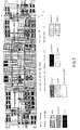
- the circuit elements to be parameterized which have been designed for the worst case, are "hidden” from the circuit, and the circuit structure thus obtained is stored as a circuit template or circuit skeleton, see FIG. 2
- the circuit elements to be parameterized are individually designed and dimensioned (designing) in a suitable manner for the respective application, in order then to be “faded in” in the circuit template in order to obtain a fully parameterized circuit in this way, see FIG. 3.
- the subcells must be designed according to the external loads, such as B. the capacitive load of the word or bit line can be adapted or parameterized in a suitable manner.
- the word decoder cell is designed for the maximum load.
- the relevant circuit elements, such as. B. inverter chains are removed from the circuit according to the invention ("hidden"), and the circuit structure thus obtained is stored as a circuit template.
- the mask information required for the circuit elements is only added to the circuit template at a later point in time (“faded in”).
- the circuit template satisfies the DRC checks that apply to the technology. If the external loads on the circuit are known for a specific application, the circuit elements can be individually adapted to the actual loads or requirements. The adapted circuit elements are together with the The circuit template is stored as the currently adapted overall circuit and used in a subsequent program sequence for physical implementation.
- the circuit template By “hiding” the circuit elements designed for the worst case, the circuit template ensures maximum space for different circuit element structures. By suitably placing the circuit elements to be parameterized or adapted at the respective edges of the circuit template, the area that is not required can be used for other purposes. This leads to a reduction in the total circuit area.
Landscapes
- Engineering & Computer Science (AREA)
- Computer Hardware Design (AREA)
- Physics & Mathematics (AREA)
- Theoretical Computer Science (AREA)
- Evolutionary Computation (AREA)
- Geometry (AREA)
- General Engineering & Computer Science (AREA)
- General Physics & Mathematics (AREA)
- Semiconductor Integrated Circuits (AREA)
- Design And Manufacture Of Integrated Circuits (AREA)
Applications Claiming Priority (2)
| Application Number | Priority Date | Filing Date | Title |
|---|---|---|---|
| DE3732851 | 1987-09-29 | ||
| DE3732851 | 1987-09-29 |
Publications (2)
| Publication Number | Publication Date |
|---|---|
| EP0309926A2 true EP0309926A2 (fr) | 1989-04-05 |
| EP0309926A3 EP0309926A3 (fr) | 1990-12-05 |
Family
ID=6337151
Family Applications (1)
| Application Number | Title | Priority Date | Filing Date |
|---|---|---|---|
| EP19880115611 Withdrawn EP0309926A3 (fr) | 1987-09-29 | 1988-09-22 | Méthode pour fabriquer des circuits, dont les paramètres peuvent être entièrement spécifiés, dans la technologie de circuits intégrés |
Country Status (2)
| Country | Link |
|---|---|
| EP (1) | EP0309926A3 (fr) |
| JP (1) | JPH01165141A (fr) |
Cited By (1)
| Publication number | Priority date | Publication date | Assignee | Title |
|---|---|---|---|---|
| EP0758624B1 (fr) * | 1995-08-11 | 2002-08-07 | Tetra Pak Plastics Limited | Installation de remplissage stérile de bouteilles suivant un cycle continu |
Families Citing this family (1)
| Publication number | Priority date | Publication date | Assignee | Title |
|---|---|---|---|---|
| HRP20160625T1 (hr) | 2007-09-10 | 2016-08-12 | Boston Biomedical, Inc. | Novi inhibitori stat3 signalnog puta i inhibitori matičnih stanica raka |
-
1988
- 1988-09-22 EP EP19880115611 patent/EP0309926A3/fr not_active Withdrawn
- 1988-09-27 JP JP63243786A patent/JPH01165141A/ja active Pending
Non-Patent Citations (3)
| Title |
|---|
| E.D.N. ELECTRICAL DESIGN NEWS, Band 28, Nr. 19, September 1983, Seiten 147-158, Boston, Mass., US; S. NANCE et al.: "Cell-layout compilers simplify custom-IC design" * |
| MICROPROCESSING & MICROPROGRAMMING, Band 18, Nr. 1-5, 1986, Seiten 445-452, Amsterdam, NL; P. FRISON et al.: "The MADMACS layout system" * |
| PROCEEDINGS OF THE IEEE 1986 CUSTOM INTEGRATED CIRCUITS CONFERENCE, Rochester, New York, 12.-15. Mai 1986, Seiten 343-346, IEEE, New York, US; S. DHOLAKIA et al.: "Compilation of standard cell libraries" * |
Cited By (1)
| Publication number | Priority date | Publication date | Assignee | Title |
|---|---|---|---|---|
| EP0758624B1 (fr) * | 1995-08-11 | 2002-08-07 | Tetra Pak Plastics Limited | Installation de remplissage stérile de bouteilles suivant un cycle continu |
Also Published As
| Publication number | Publication date |
|---|---|
| EP0309926A3 (fr) | 1990-12-05 |
| JPH01165141A (ja) | 1989-06-29 |
Similar Documents
| Publication | Publication Date | Title |
|---|---|---|
| DE69526811T2 (de) | Integrierte Halbleiterschaltung mit zwei Versorgungsspannungen | |
| DE3855158T2 (de) | Dekodier-verfahren und -system für Befehle mit verschiedenen unvereinbaren Formaten | |
| DE69315576T2 (de) | Verfahren und testanlage zur entwicklung einer integrierten schaltung. | |
| DE10051021B4 (de) | System, Verfahren und Computerprogramm zur Bereitstellung interaktiver Web-Inhalte in statisch verknüpften Dateien | |
| DE69331085T2 (de) | Automatisiertes LSI-Entwurfsystem und Verfahren | |
| EP0520083A1 (fr) | Protection de la consistance des données dans un système de télécommunications numériques | |
| DE4426001A1 (de) | Verfahren zur Überlastvermeidung bei einem Systemanlauf eines Mehrrechnersystems und Mehrrechnersystem dafür | |
| DE10212634A1 (de) | Seitenbeschreibungssprache, die für ein direktes Drucken von Mehr-Datei-Formaten ausgelegt ist | |
| DE19535519A1 (de) | Verfahren zur Reduzierung des Umfanges von Computerprogrammen | |
| EP1005215B1 (fr) | Procédé et système pour l'édition des données de configuration pour systèmes de télécommunication | |
| DE19904333B4 (de) | Informationsverarbeitungsverfahren und Informationsverarbeitungsvorrichtung mit einer Unterbrechungssteuerungsfunktion mit Prioritätswertigkeiten | |
| EP1005216A2 (fr) | Procédé et système pour validation des données de configuration pour systèmes de télécommunication | |
| EP0309926A2 (fr) | Méthode pour fabriquer des circuits, dont les paramètres peuvent être entièrement spécifiés, dans la technologie de circuits intégrés | |
| DE102004057727A1 (de) | Engineeringsystem mit automatischer Generierung von Instanzvorlagen | |
| EP1248430B1 (fr) | Méthode et dispositif de génération de masques filtrants pour vérifier l'importance de caractéristiques | |
| EP1235123A2 (fr) | Méchanisme rapporté pour un système de commande basé sur un champ de données de type | |
| EP0560342B1 (fr) | Méthode pour le débogage de programmes HDL | |
| DE69206633T2 (de) | Verfahren und rechnersystem zur datenuebertragung. | |
| DE2952689A1 (de) | Programmierbarer lesespeicher-addierer | |
| DE2836873C2 (de) | Speichersystem mit wahlfreiem Zugriff | |
| DE10128959A1 (de) | Addon-Mechanismus für ein Steuerungssystem basierend auf einem Typdatenfeld | |
| DE69329174T2 (de) | Kompilierungsmechanismus für ein Simulationsmodell | |
| DE19906177C1 (de) | Verfahren und Vorrichtung zur Übertragung von Simulationsmodellen zwischen Simulatoren | |
| DE4408106A1 (de) | Verfahren zur Simulation einer in EDIF beschriebenen Schaltung mit einem VHDL-Simulator auf einem Rechner | |
| DE10105729C1 (de) | Verfahren und System zur funktionsmäßigen Erweiterung einer Telekommunikationsanlage |
Legal Events
| Date | Code | Title | Description |
|---|---|---|---|
| PUAI | Public reference made under article 153(3) epc to a published international application that has entered the european phase |
Free format text: ORIGINAL CODE: 0009012 |
|
| AK | Designated contracting states |
Kind code of ref document: A2 Designated state(s): AT BE CH DE FR GB IT LI LU NL SE |
|
| PUAL | Search report despatched |
Free format text: ORIGINAL CODE: 0009013 |
|
| AK | Designated contracting states |
Kind code of ref document: A3 Designated state(s): AT BE CH DE FR GB IT LI LU NL SE |
|
| 17P | Request for examination filed |
Effective date: 19901205 |
|
| STAA | Information on the status of an ep patent application or granted ep patent |
Free format text: STATUS: THE APPLICATION HAS BEEN WITHDRAWN |
|
| 18W | Application withdrawn |
Withdrawal date: 19910228 |
|
| R18W | Application withdrawn (corrected) |
Effective date: 19910228 |