EP0310047A2 - Doppel-diffundierter MOSFET - Google Patents
Doppel-diffundierter MOSFET Download PDFInfo
- Publication number
- EP0310047A2 EP0310047A2 EP88116031A EP88116031A EP0310047A2 EP 0310047 A2 EP0310047 A2 EP 0310047A2 EP 88116031 A EP88116031 A EP 88116031A EP 88116031 A EP88116031 A EP 88116031A EP 0310047 A2 EP0310047 A2 EP 0310047A2
- Authority
- EP
- European Patent Office
- Prior art keywords
- semiconductor regions
- regions
- semiconductor
- region
- periphery
- Prior art date
- Legal status (The legal status is an assumption and is not a legal conclusion. Google has not performed a legal analysis and makes no representation as to the accuracy of the status listed.)
- Withdrawn
Links
Images


Classifications
-
- H—ELECTRICITY
- H10—SEMICONDUCTOR DEVICES; ELECTRIC SOLID-STATE DEVICES NOT OTHERWISE PROVIDED FOR
- H10D—INORGANIC ELECTRIC SEMICONDUCTOR DEVICES
- H10D84/00—Integrated devices formed in or on semiconductor substrates that comprise only semiconducting layers, e.g. on Si wafers or on GaAs-on-Si wafers
- H10D84/01—Manufacture or treatment
- H10D84/0123—Integrating together multiple components covered by H10D12/00 or H10D30/00, e.g. integrating multiple IGBTs
- H10D84/0126—Integrating together multiple components covered by H10D12/00 or H10D30/00, e.g. integrating multiple IGBTs the components including insulated gates, e.g. IGFETs
- H10D84/0135—Manufacturing their gate conductors
- H10D84/014—Manufacturing their gate conductors the gate conductors having different materials or different implants
-
- H—ELECTRICITY
- H10—SEMICONDUCTOR DEVICES; ELECTRIC SOLID-STATE DEVICES NOT OTHERWISE PROVIDED FOR
- H10D—INORGANIC ELECTRIC SEMICONDUCTOR DEVICES
- H10D30/00—Field-effect transistors [FET]
- H10D30/60—Insulated-gate field-effect transistors [IGFET]
- H10D30/64—Double-diffused metal-oxide semiconductor [DMOS] FETs
- H10D30/66—Vertical DMOS [VDMOS] FETs
-
- H—ELECTRICITY
- H10—SEMICONDUCTOR DEVICES; ELECTRIC SOLID-STATE DEVICES NOT OTHERWISE PROVIDED FOR
- H10D—INORGANIC ELECTRIC SEMICONDUCTOR DEVICES
- H10D62/00—Semiconductor bodies, or regions thereof, of devices having potential barriers
- H10D62/10—Shapes, relative sizes or dispositions of the regions of the semiconductor bodies; Shapes of the semiconductor bodies
- H10D62/124—Shapes, relative sizes or dispositions of the regions of semiconductor bodies or of junctions between the regions
- H10D62/126—Top-view geometrical layouts of the regions or the junctions
- H10D62/127—Top-view geometrical layouts of the regions or the junctions of cellular field-effect devices, e.g. multicellular DMOS transistors or IGBTs
-
- H—ELECTRICITY
- H10—SEMICONDUCTOR DEVICES; ELECTRIC SOLID-STATE DEVICES NOT OTHERWISE PROVIDED FOR
- H10D—INORGANIC ELECTRIC SEMICONDUCTOR DEVICES
- H10D64/00—Electrodes of devices having potential barriers
- H10D64/20—Electrodes characterised by their shapes, relative sizes or dispositions
- H10D64/23—Electrodes carrying the current to be rectified, amplified, oscillated or switched, e.g. sources, drains, anodes or cathodes
- H10D64/251—Source or drain electrodes for field-effect devices
- H10D64/258—Source or drain electrodes for field-effect devices characterised by the relative positions of the source or drain electrodes with respect to the gate electrode
-
- H—ELECTRICITY
- H10—SEMICONDUCTOR DEVICES; ELECTRIC SOLID-STATE DEVICES NOT OTHERWISE PROVIDED FOR
- H10D—INORGANIC ELECTRIC SEMICONDUCTOR DEVICES
- H10D64/00—Electrodes of devices having potential barriers
- H10D64/20—Electrodes characterised by their shapes, relative sizes or dispositions
- H10D64/27—Electrodes not carrying the current to be rectified, amplified, oscillated or switched, e.g. gates
- H10D64/311—Gate electrodes for field-effect devices
- H10D64/411—Gate electrodes for field-effect devices for FETs
- H10D64/511—Gate electrodes for field-effect devices for FETs for IGFETs
- H10D64/517—Gate electrodes for field-effect devices for FETs for IGFETs characterised by the conducting layers
- H10D64/519—Gate electrodes for field-effect devices for FETs for IGFETs characterised by the conducting layers characterised by their top-view geometrical layouts
Definitions
- the present invention relates to a double-diffused MOS FET used mainly for power control.
- a double-diffused MOS FET is generally used for power control, and is constituted by a plurality of unit FET cells connected in parallel.
- Fig. 1 is a plan view showing an arrangement of a conventional D-MOS comprising unit FET cells each having a square top surface
- Fig. 2 is a sectional view taken along line A - A′ of Fig. 1.
- low-concentration n-type epitaxial layer 11 is deposited on a surface of high-concentration n-type silicon substrate 10.
- Substrate 10 and epitaxial layer 11 together constitute a drain region of each unit FET cell.
- P+-type low-resistance regions 12 are formed separately at a plurality of positions on the surface of epitaxial layer 11, and p-type channel base regions 13 are respectively formed around regions 12.
- N+-type source region 14 is continuously formed on the surfaces of each low-resistance region 12 and each channel base region 13.
- a gate electrode 16 is formed on the surface of each channel base region 13, through gate insulating layer 15, and is patterned in the form of a mesh constituted by a plurality of square openings 17.
- reference numeral 18 denotes a source electrode which is connected to each of low-resistance regions 12 and source regions 14, and which is common to all the unit FET cells.
- drain electrode 19 is connected to the other surface of substrate 10.
- npn bipolar transistor Q constituted by n-type epitaxial region 11 as a collector, p-type channel base region 12 as a base, and source region 14 as an emitter is parasitically generated. Furthermore, parasitic resistance Rb due to a diffusion resistance in low-concentration channel base region 13 is formed between the base and emitter of transistor Q.
- low-resistance region 12 and channel base region 13 are respectively formed into square patterns. Being formed in this manner, the distance between the peripheries of region 12 and channel base region 13 which is located outward therefrom, is quite large at the respective corners of the unit FET cell. As a result, the value of parasitic resistance Rb varies depending on positions in the unit FET cell. For example, the distance from the periphery of low-resistance region 12 to that of channel base region 13, located outward therefrom, becomes relatively small at a position along line a - a′ in Fig. 4. For this reason, the value of parasitic resistance Rb at this position becomes relatively small.
- the present invention has been developed in consideration of the above situation, and has as its object to provide a double-diffused MOS FET has good resistance to destruction caused when a parasitic bipolar transistor is rendered conductive.
- a double-diffused MOS FET comprising a semiconductor substrate having parallel first and second planar surfaces and doped with an impurity of a first conductivity type, a plurality of first semiconductor regions of a second conductivity type, diffused in the form of a mesh in the first planar surface of the substrate, each of the first semiconductor regions having a substantially square periphery with four rounded corners, a plurality of second semiconductor regions of the second conductivity type, each of which is diffused so as to surround a corresponding one of the first semiconductor regions, has a depth less than that of the first semiconductor region, and has a periphery the shape of which corresponds to that of the first semiconductor region, the planar distance from the periphery of each of the first second semiconductor regions to that of a corresponding one of the first semiconductor regions being set to be equal throughout the periphery of each of the first semiconductor regions, a plurality of source regions
- Reference numeral 20 denotes a silicon semiconductor layer.
- Antimony or arsenic is doped as an n-type impurity in semiconductor layer 20, at a concentration of, for example, about 1 x 10¹⁸ to 1 x 10²⁰ (/cm3).
- Semiconductor layer 20 and epitaxial layer 21 constitute n-type substrate 22.
- Semiconductor layer 20 and epitaxial layer 21 serve as a drain for a plurality of unit FETs to be described later.
- P+-type low-resistance regions 23 are formed separately in a plurality of portions of the exposed surface of n-type epitaxial layer 21, and are doped with boron, as a p-type impurity, is doped at a surface concentration of about 1 x 10²⁰ (/cm3).
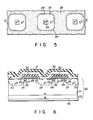
- Low-resistance regions 23 are formed on the exposed surface of n-type epitaxial layer 21 in the form of a mesh, as shown in Fig. 5.
- P-type channel base regions 24 each having a depth less than that of each low-resistance region 23 are respectively formed around low-resistance regions 23. Boron as a p-type impurity is doped in each channel base region 24 at a surface concentration of about 1 .
- a plurality of n-type source regions 25 each having a depth smaller than that of each channel base region 24 are continuously formed on the surfaces of low-resistance regions 23 and channel base regions 24, respectively.
- Each source region 25 is formed such that its periphery is located inward from that of a corresponding channel base region 24 while a predetermined distance is kept between these peripheries.
- Surface region 26 of channel base region 24, which is present between the peripheries of each source region 25 and corresponding channel base region 24, is defined as a channel region of each unit FET cell. Therefore, channel regions 26 of the unit FET cells are formed so as to surround corresponding channel base regions 24.
- Gate insulating layer 27 consisting of silicon oxide is deposited in the form of a mesh so as to surround channel base regions 24 and low-resistance regions 23 and cover channel regions 26 described above.
- gate electrode 28 consisting of polysilicon and having the same shape as that of gate insulating layer 27 is deposited on gate insulating layer 27. As shown in Fig. 5, gate insulating layer 27 and gate electrode 28 formed into the same shape are patterned in the form of a mesh constituted by a plurality of substantially square openings 29 each having rounded four corners.
- a plurality of unit FET cells each constituted by n-type silicon semiconductor and n-type epitaxial layers 20 and 21 as a drain, channel base region 24 as a base, and source region 25 as a source are formed near openings 29.
- Insulating interlayer 30 is deposited on gate electrode 28.
- Source electrode 31 consisting of aluminum is integrally formed on the exposed surfaces of low-resistance regions 23 and source regions 25, so that all source regions 25 are connected to source electrode 31.
- surface protective layer 32 consisting of silicon oxide or silicon nitride is deposited on source electrode 31 by CVD.
- Drain electrode 33 consisting of aluminum is formed on the exposed surface of n-type silicon semiconductor layer 20. Note that each low-resistance region 23 is formed so as to decrease the value of parasitic resistance Rb due to a diffusion resistance between the base and the emitter of parasitic bipolar transistor Q.
- Channel base region 24 is formed by p-type impurity diffusion using gate electrode 28 as a mask. Furthermore, low-resistance region 23 is formed into a shape similar to opening 29. Low-resistance regions 23 are formed by p-type impurity diffusion using a mask (not shown) for impurity diffusion, which has a plurality of openings smaller than openings 29. Then, the mask which is used for forming low-resistance regions 23 is removed.
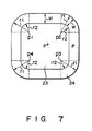
- Fig. 7 is a plan view showing a pattern of channel base region 24 and low-resistance region 23 of one unit FET in the D-MOS of the above embodiment.
- the peripheries of low-resistance region 23 and channel base region 24 are formed into substantially square shapes similar to each other.
- the four corners of regions 23 and 24 respectively constitute parts of concentrical circles respectively defined by radii r1 and r2, and points p1, p2, p3, and p4 as the centers.
- Distance W from the periphery of low-resistance region 23 to that of channel base region 24 is set to be constant at any positions.
- the value of parasitic resistance Rb between the base and the emitter of the bipolar transistor corresponding to parasitic bipolar transistor Q shown in Fig. 3 is set to be constant at any positions in each unit FET.
- the parasitic transistors are turned on in the same manner at any positions in each unit FET, thus solving the problem that only some of the transistors are easily rendered conductive as in the conventional D-MOS.
- the D-MOS of this embodiment has good resistance to destruction caused when an inductive load is driven.
- the D-MOS of this embodiment can be manufactured by only changing the shape of mask pattern for diffusion without specifically adding complex manufacturing processes.
Landscapes
- Insulated Gate Type Field-Effect Transistor (AREA)
- Semiconductor Integrated Circuits (AREA)
- Metal-Oxide And Bipolar Metal-Oxide Semiconductor Integrated Circuits (AREA)
Applications Claiming Priority (2)
| Application Number | Priority Date | Filing Date | Title |
|---|---|---|---|
| JP62246013A JPS6489465A (en) | 1987-09-30 | 1987-09-30 | Double-diffusion type mos field effect transistor |
| JP246013/87 | 1987-09-30 |
Publications (2)
| Publication Number | Publication Date |
|---|---|
| EP0310047A2 true EP0310047A2 (de) | 1989-04-05 |
| EP0310047A3 EP0310047A3 (de) | 1990-01-31 |
Family
ID=17142161
Family Applications (1)
| Application Number | Title | Priority Date | Filing Date |
|---|---|---|---|
| EP88116031A Withdrawn EP0310047A3 (de) | 1987-09-30 | 1988-09-28 | Doppel-diffundierter MOSFET |
Country Status (3)
| Country | Link |
|---|---|
| EP (1) | EP0310047A3 (de) |
| JP (1) | JPS6489465A (de) |
| KR (1) | KR910008714B1 (de) |
Cited By (12)
| Publication number | Priority date | Publication date | Assignee | Title |
|---|---|---|---|---|
| US5521409A (en) * | 1990-12-21 | 1996-05-28 | Siliconix Incorporated | Structure of power mosfets, including termination structures |
| EP0776048A3 (de) * | 1995-11-21 | 1998-07-29 | Fuji Electric Co., Ltd. | MOS-Gate-Anordnung-Basiszone mit hoher Durchschlagsfestigkeit |
| WO1999007018A1 (de) * | 1997-07-31 | 1999-02-11 | Siemens Aktiengesellschaft | Halbleiterstruktur auf basis von silizium-carbid-material mit mehreren elektrisch unterschiedlichen teilgebieten |
| EP0492991B1 (de) * | 1990-12-21 | 1999-06-23 | SILICONIX Incorporated | Verfahren zur Herstellung von doppelt-diffundierten integrierten MOSFET-Zellen |
| EP1029363A2 (de) * | 1997-11-13 | 2000-08-23 | Abb Research Ltd. | Sic halbleiteranordnung und sic transistor mit isolierter steuerelektrode |
| US9431249B2 (en) | 2011-12-01 | 2016-08-30 | Vishay-Siliconix | Edge termination for super junction MOSFET devices |
| US9484451B2 (en) | 2007-10-05 | 2016-11-01 | Vishay-Siliconix | MOSFET active area and edge termination area charge balance |
| US9508596B2 (en) | 2014-06-20 | 2016-11-29 | Vishay-Siliconix | Processes used in fabricating a metal-insulator-semiconductor field effect transistor |
| US9614043B2 (en) | 2012-02-09 | 2017-04-04 | Vishay-Siliconix | MOSFET termination trench |
| US9842911B2 (en) | 2012-05-30 | 2017-12-12 | Vishay-Siliconix | Adaptive charge balanced edge termination |
| US9882044B2 (en) | 2014-08-19 | 2018-01-30 | Vishay-Siliconix | Edge termination for super-junction MOSFETs |
| US9887259B2 (en) | 2014-06-23 | 2018-02-06 | Vishay-Siliconix | Modulated super junction power MOSFET devices |
Families Citing this family (1)
| Publication number | Priority date | Publication date | Assignee | Title |
|---|---|---|---|---|
| JP5687128B2 (ja) * | 2011-05-06 | 2015-03-18 | 三菱電機株式会社 | 半導体装置およびその製造方法 |
Family Cites Families (2)
| Publication number | Priority date | Publication date | Assignee | Title |
|---|---|---|---|---|
| US4639762A (en) * | 1984-04-30 | 1987-01-27 | Rca Corporation | MOSFET with reduced bipolar effects |
| JPS6180859A (ja) * | 1984-09-28 | 1986-04-24 | Hitachi Ltd | パワ−mosfet |
-
1987
- 1987-09-30 JP JP62246013A patent/JPS6489465A/ja active Pending
-
1988
- 1988-09-28 EP EP88116031A patent/EP0310047A3/de not_active Withdrawn
- 1988-09-30 KR KR1019880012751A patent/KR910008714B1/ko not_active Expired
Cited By (17)
| Publication number | Priority date | Publication date | Assignee | Title |
|---|---|---|---|---|
| EP0492991B1 (de) * | 1990-12-21 | 1999-06-23 | SILICONIX Incorporated | Verfahren zur Herstellung von doppelt-diffundierten integrierten MOSFET-Zellen |
| US5521409A (en) * | 1990-12-21 | 1996-05-28 | Siliconix Incorporated | Structure of power mosfets, including termination structures |
| EP0776048A3 (de) * | 1995-11-21 | 1998-07-29 | Fuji Electric Co., Ltd. | MOS-Gate-Anordnung-Basiszone mit hoher Durchschlagsfestigkeit |
| WO1999007018A1 (de) * | 1997-07-31 | 1999-02-11 | Siemens Aktiengesellschaft | Halbleiterstruktur auf basis von silizium-carbid-material mit mehreren elektrisch unterschiedlichen teilgebieten |
| US6225680B1 (en) | 1997-07-31 | 2001-05-01 | Siced Electronics Development Gmbh & Co. Kg | Semiconductor structure based on silicon carbide material, with a plurality electrically different partial regions |
| EP1029363A2 (de) * | 1997-11-13 | 2000-08-23 | Abb Research Ltd. | Sic halbleiteranordnung und sic transistor mit isolierter steuerelektrode |
| US9484451B2 (en) | 2007-10-05 | 2016-11-01 | Vishay-Siliconix | MOSFET active area and edge termination area charge balance |
| US9431249B2 (en) | 2011-12-01 | 2016-08-30 | Vishay-Siliconix | Edge termination for super junction MOSFET devices |
| US9935193B2 (en) | 2012-02-09 | 2018-04-03 | Siliconix Technology C. V. | MOSFET termination trench |
| US9614043B2 (en) | 2012-02-09 | 2017-04-04 | Vishay-Siliconix | MOSFET termination trench |
| US9842911B2 (en) | 2012-05-30 | 2017-12-12 | Vishay-Siliconix | Adaptive charge balanced edge termination |
| US10229988B2 (en) | 2012-05-30 | 2019-03-12 | Vishay-Siliconix | Adaptive charge balanced edge termination |
| US9508596B2 (en) | 2014-06-20 | 2016-11-29 | Vishay-Siliconix | Processes used in fabricating a metal-insulator-semiconductor field effect transistor |
| US9887259B2 (en) | 2014-06-23 | 2018-02-06 | Vishay-Siliconix | Modulated super junction power MOSFET devices |
| US10283587B2 (en) | 2014-06-23 | 2019-05-07 | Vishay-Siliconix | Modulated super junction power MOSFET devices |
| US9882044B2 (en) | 2014-08-19 | 2018-01-30 | Vishay-Siliconix | Edge termination for super-junction MOSFETs |
| US10340377B2 (en) | 2014-08-19 | 2019-07-02 | Vishay-Siliconix | Edge termination for super-junction MOSFETs |
Also Published As
| Publication number | Publication date |
|---|---|
| JPS6489465A (en) | 1989-04-03 |
| EP0310047A3 (de) | 1990-01-31 |
| KR890005895A (ko) | 1989-05-17 |
| KR910008714B1 (ko) | 1991-10-19 |
Similar Documents
| Publication | Publication Date | Title |
|---|---|---|
| EP2302683B1 (de) | Feldeffekt-halbleiteranordnung und verfahren zu ihrer herstellung | |
| US4931846A (en) | Vertical MOSFET having voltage regulator diode at shallower subsurface position | |
| US6724044B2 (en) | MOSFET device having geometry that permits frequent body contact | |
| US6657262B2 (en) | Monolithically integrated electronic device and fabrication process therefor | |
| US5897355A (en) | Method of manufacturing insulated gate semiconductor device to improve ruggedness | |
| US5451531A (en) | Method of fabricating an insulated gate semiconductor device | |
| US4779123A (en) | Insulated gate transistor array | |
| EP0310047A2 (de) | Doppel-diffundierter MOSFET | |
| JP7526010B2 (ja) | 半導体装置 | |
| US4975751A (en) | High breakdown active device structure with low series resistance | |
| US5091336A (en) | Method of making a high breakdown active device structure with low series resistance | |
| JP2635044B2 (ja) | 半導体デバイス | |
| US5786622A (en) | Bipolar transistor with a ring emitter | |
| US6563169B1 (en) | Semiconductor device with high withstand voltage and a drain layer having a highly conductive region connectable to a diffused source layer by an inverted layer | |
| JP2001007322A (ja) | 高破壊耐量電界効果型トランジスタ | |
| JP2002141505A (ja) | 電界効果トランジスタ | |
| JP3099917B2 (ja) | 電界効果トランジスタ | |
| US4599635A (en) | Semiconductor integrated circuit device and method of producing same | |
| JPH01238174A (ja) | 縦型mosfet | |
| US6459128B1 (en) | Field-effect transistor | |
| JPH0621359A (ja) | 深いp型本体接触ソースプラグを備えた電界効果トランジスタ | |
| KR102417149B1 (ko) | 전력 반도체 소자 | |
| JP2988047B2 (ja) | 半導体装置 | |
| KR102369057B1 (ko) | 전력 반도체 소자 및 그 제조 방법 | |
| KR0118637Y1 (ko) | 집적주입 논리회로소자 |
Legal Events
| Date | Code | Title | Description |
|---|---|---|---|
| PUAI | Public reference made under article 153(3) epc to a published international application that has entered the european phase |
Free format text: ORIGINAL CODE: 0009012 |
|
| 17P | Request for examination filed |
Effective date: 19881025 |
|
| AK | Designated contracting states |
Kind code of ref document: A2 Designated state(s): DE FR GB IT |
|
| PUAL | Search report despatched |
Free format text: ORIGINAL CODE: 0009013 |
|
| AK | Designated contracting states |
Kind code of ref document: A3 Designated state(s): DE FR GB IT |
|
| 17Q | First examination report despatched |
Effective date: 19911022 |
|
| STAA | Information on the status of an ep patent application or granted ep patent |
Free format text: STATUS: THE APPLICATION IS DEEMED TO BE WITHDRAWN |
|
| 18D | Application deemed to be withdrawn |
Effective date: 19920505 |