EP0310457B1 - Digitaler Vormodulationsfilter - Google Patents
Digitaler Vormodulationsfilter Download PDFInfo
- Publication number
- EP0310457B1 EP0310457B1 EP88309216A EP88309216A EP0310457B1 EP 0310457 B1 EP0310457 B1 EP 0310457B1 EP 88309216 A EP88309216 A EP 88309216A EP 88309216 A EP88309216 A EP 88309216A EP 0310457 B1 EP0310457 B1 EP 0310457B1
- Authority
- EP
- European Patent Office
- Prior art keywords
- signal
- digital
- filter
- coupled
- modulation
- Prior art date
- Legal status (The legal status is an assumption and is not a legal conclusion. Google has not performed a legal analysis and makes no representation as to the accuracy of the status listed.)
- Expired - Lifetime
Links
- 230000006870 function Effects 0.000 claims description 23
- 230000002902 bimodal effect Effects 0.000 claims description 19
- 238000003491 array Methods 0.000 claims description 17
- 238000005316 response function Methods 0.000 claims description 13
- 230000004044 response Effects 0.000 claims description 12
- 238000005070 sampling Methods 0.000 claims description 3
- 210000000352 storage cell Anatomy 0.000 claims 3
- 210000004027 cell Anatomy 0.000 claims 1
- 238000001914 filtration Methods 0.000 claims 1
- 230000008672 reprogramming Effects 0.000 claims 1
- 238000000034 method Methods 0.000 description 20
- 230000008569 process Effects 0.000 description 11
- 238000010586 diagram Methods 0.000 description 10
- 238000007792 addition Methods 0.000 description 6
- 238000006243 chemical reaction Methods 0.000 description 5
- 238000009825 accumulation Methods 0.000 description 4
- 238000004891 communication Methods 0.000 description 3
- 230000008520 organization Effects 0.000 description 3
- 238000001228 spectrum Methods 0.000 description 2
- 230000003321 amplification Effects 0.000 description 1
- 230000008901 benefit Effects 0.000 description 1
- 230000005540 biological transmission Effects 0.000 description 1
- 230000003750 conditioning effect Effects 0.000 description 1
- 238000012937 correction Methods 0.000 description 1
- 238000013461 design Methods 0.000 description 1
- 238000012986 modification Methods 0.000 description 1
- 230000004048 modification Effects 0.000 description 1
- 238000003199 nucleic acid amplification method Methods 0.000 description 1
- 238000013139 quantization Methods 0.000 description 1
- 238000012546 transfer Methods 0.000 description 1
Images


Classifications
-
- H—ELECTRICITY
- H03—ELECTRONIC CIRCUITRY
- H03H—IMPEDANCE NETWORKS, e.g. RESONANT CIRCUITS; RESONATORS
- H03H17/00—Networks using digital techniques
- H03H17/02—Frequency selective networks
- H03H17/0294—Variable filters; Programmable filters
-
- H—ELECTRICITY
- H03—ELECTRONIC CIRCUITRY
- H03H—IMPEDANCE NETWORKS, e.g. RESONANT CIRCUITS; RESONATORS
- H03H17/00—Networks using digital techniques
- H03H17/02—Frequency selective networks
- H03H17/06—Non-recursive filters
- H03H17/0607—Non-recursive filters comprising a ROM addressed by the input data signals
Definitions
- the present invention relates generally to transmitters for transmitting angle modulated signals, and, more particularly, to a digital premodulation filter for conditioning a serial bit stream prior to frequency (or phase) modulation of a RF carrier signal.
- a disadvantage of frequency modulation (FM) is however that the spectrum is rather wide.
- a solution is to use spectrally efficient modulation to maximize the bandwidth efficiency, measured in bits/second/Hz.
- a method for achieving spectrally efficient modulation is to shape the data at the input of the frequency modulator by means of a premodulation filter.
- a premodulation filter is described in the article "Tamed Frequency Modulation, A Novel Method to Achieve Spectrum Economy in Digital Transmission” by F. deJager and C.B. Dekker, published in "IEEE Transactions on Communications" Vol. Com. 26 No. 5, May, 1978.
- the modulation described in this article relates to what is commonly referred to as tamed frequency modulation (TFM).
- the premodulation filter comprises a Gaussian low-pass filter and a correction filter.
- the latter filter comprises a cascade of 2n delay sections, each having a time delay of T seconds.
- the output of the premodulation filter is connected to the signal input of a frequency modulation circuit to provide the modulated output as desired.
- the premodulation filter comprises the series arrangement of a non-recursive second order digital filter with three weighting factors, two of which are equal to each other, and a low pass filter realized by means of a "raised cosine" filter which satisfies the first Nyquist criterion.
- the mutually unequal weighting factors have the values A and B, the value of the weighting factor A and, respectively of the non-recursive second order filter being less than one-fourth and larger than one-half, respectively, 2A + B being equal to one and the roll off coefficient of the "raised cosine" filter being unequal to zero.
- premodulation filter circuits comprising analog filters or a combination of digital and analog filters to provide carrier modulation dedicated to a single modulation type; TFM, for example.
- CPM continuous phase modulation
- Examples of such CPM are minimum shift keying (MSK), Gaussian minimum shift keying (GMSK), tamed frequency modulation (TFM) and four-level FM (4-FM) and additional modulation methods which a user may define.
- the premodulation filter of the present invention is electronically configurable by a user to perform a desired modulation type, thus providing a more versatile instrument than previous methods which are typically dedicated to a single modulation type.
- the premodulation filter utilizes a finite impulse response filter (FIR) technique to digitally filter an input serial bit data stream.
- FIR finite impulse response filter
- Each modulation format such as TFM, has a unique impulse response function g(t) which is the response to a single input data bit represented by a single impulse function.
- the premodulation filter preforms a linear combination of g(t) responses resulting from the input data stream represented by a series of bimodal impulse functions.
- the output of FIR digital filter in the form of parallel digital words is coupled to a digital to analog converter (DAC).
- DAC digital to analog converter
- the output of the DAC is then passed through an analog filter to provide a smooth analog voltage input to a modulator to vary, for example, the frequency or phase of an oscillator, such as a voltage controlled oscillator (VCO) to provide a digitally modulated carrier output.
- a modulator such as a voltage controlled oscillator (VCO) to provide a digitally modulated carrier output.
- VCO voltage controlled oscillator
- the prior art premodulation filters described hereinabove are typically dedicated to a single digital modulation format and are not easily user configurable.
- a number of frequency or phase pulse-shape function g(t) arrays are stored in ROM (or RAM) allowing the user to easily choose any desired modulation format.
- a user may adjust operational parameters to optimize further performance or to design a custom modulation format for use with a user's particular digital communication system.
- prior art digital premodulation FIR filters typically utilize multiplication in the convolution process whereas the present invention utilizes an adder thus providing a speed advantage over the prior art.
- Figure 1 is a block diagram illustrating an RF transmitter utilizing FM modulation and of an RF transmitter utilizing phase modulation.
- Figure 2 is a block diagram illustrating an RF transmitter utilizing I-Q modulation.
- Figure 3 is a block diagram illustrating a conceptual representation of a FIR digital premodulation filter according to the principals of the present invention.
- Figure 4 is a graphical presentation of an example of a two-level digital modulation impulse response function g(t) and algorithm utilized in the apparatus shown in Figure 6.
- Figure 5 is graphical representation of an example of a four-level digital modulation impulse response function g(t) and algorithm utilized in the apparatus shown in Figure 7.
- Figure 6 is a block diagram illustrating the implementation of the FIR premodulation filter algorithm shown in Figure 4 for two-level digital modulation.
- Figure 7 is block diagram illustrating the implementation of the FIR premodulation filter algorithm shown in Figure 5 for two-level or four-level digital modulation.
- the method and apparatus described herein utilizes a Finite Impulse Response (FIR) technique to digitally filter an input data signal.
- the FIR digital premodulation filter is programmable by the user to generate various modulation signals corresponding to several different types of frequency modulation (FM) and phase modulation (PM). Each modulation type or format has a unique impulse response function g(t) which is the response to a single input data impulse.
- the FIR digital premodulation filter performs a convolution utilizing a linear combination of g(t) responses resulting from the input data stream.
- the input to the FIR digital premodulation filter is in the form of a bimodal impulse stream which represents the input data.
- FIG. 1A and 1B a block diagram illustrating a portion 10 of a signal generator which provides a frequency modulated RF carrier signal is shown. It comprises a digital premodulation filter 11 having an input line 17 for receiving a data signal, and an RF carrier generator 15 coupled to a frequency modulator 13. By means of the digital premodulation filter 11, which will be described in greater detail, an analog modulation signal is generated. This modulation signal is coupled to the modulator 13 to frequency modulate the RF carrier signal supplied by the RF carrier generator 15. The FM RF output signal thus formed by modulator 13 is output on line 19.
- Fig. 1A represents a frequency modulation system wherein the FIR function g(t) utilized by the digital premodulation filter 11 represents the instantaneous frequency deviation of the RF carrier output signal on line 19 resulting from a single impulse function and can be termed a "frequency pulse shape function”.
- Fig. 1B represents a phase modulation system wherein the FIR function g(t) utilized by the digital premodulation filter 11 represents the instantaneous phase deviation of the RF carrier output signal on line 19 resulting from a single impulse function and can be termed "phase pulse shape function".
- a multiple-phase modulation system 20 including an inphase (I) channel and a quadrature (Q) channel (I-Q modulator) is shown.
- FIR digital premodulation filter 23 may be programmed to generate a desired type of modulation wherein g(t) will represent either the instantaneous frequency or phase deviation of the RF output signal resulting from a single impulse function, depending on whether FM or PM operation is used.
- a input data stream on line 21 is coupled to the FIR digital premodulation filter 23 which performs a convolution utilizing a linear combination of g(t) responses and outputs a signal in the form of parallel digital words.
- the output of the FIR digital premodulation filter 23 is coupled via switch 25 to a modulo 2 PI transform network and accumulator 27 to transform the instantaneous frequency deviation to an instantaneous phase deviation.
- the accumulator 27 output is coupled via switch 31 to a cosine-weighted DAC 33 and an analog reconstruction filter 35 to provide the analog signal for the I channel modulator 45.
- the accumulator 27 output signal is coupled to a sine-weighted DAC 37 and analog reconstruction filter 39 to provide the analog signal to the Q channel modulator 47.
- the output of the FIR digital premodulation filter 23 is coupled to a modulo 2 PI transform network 29 to provide the modulation signal representing instantaneous phase deviation.
- the transform network 29 output signal is coupled via switch 31 to the I channel and Q channel modulators 45 and 47, respectively.
- the RF carrier signal generated by RF frequency source 41 is coupled to both I and Q channel modulators 45, 47 to be modulated in a conventional manner and provide an RF output signal on line 55 at the output of adder 53.
- FIG. 3 a schematic drawing which illustrates a conceptual representation of the classical convolution operation of the FIR digital premodulation filter of Figs. 1 and 2 is shown.
- a serial logic level input data stream on line 61 is converted to binary numbers by converter 63 and converter 64.
- the value of each binary number represents the magnitude and sign of a corresponding bimodal data impulse.
- Converter 63 performs the conversion for two-level modulation formats such as MSK, GMSK, and TFM.
- two-level modulation as shown in Table 1, a logical 1 input data bit may be represented by a binary number of value 1 (base 10) which corresponds to a bimodal data impulse of value +1.
- a logical 0 data bit may be represented by a binary number of value -1 (base 10) which corresponds to a bimodal data impulse of value -1.
- Table 1 Two-Level Conversion Logical Level Input Data Bit Value Binary Number (base 10) 0 -1 1 1
- Converter 64 performs the conversion for four-level modulation formats such as 4-FM.
- pairs of serial data bits are represented by binary numbers of value -1, -1/3, 1/3 or 1 (base 10) which correspond to bimodal data impulses of values -1, -1/3, 1/3, and +1 respectively.
- Table 2 Four-Level Conversion Pairs of Serial Logical Level Input Data Bits Value of Binary Number (base 10) 00 1 01 1/3 11 -1/3 10 -1
- Switch 65 selects either two- or four-level operation. It is shown for illustration purposes in the four-level position and four-level binary numbers are present in shift register 67.
- Curve 74 is a graphical representation of a selected one of several g(t) impulse response functions corresponding to different modulation formats stored as digital binary arrays in a ROM or RAM 71.
- a desired modulation format may be selected by a user via external control lines 75 coupled to the address block 72.
- the xq data clock 77 is phase locked to the data clock 73 with frequency of data clock 73 * q.
- the binary numbers which represent the input data stream are convolved with the stored binary numbers which represent the selected impulse response function g(t).
- the convolution involves multiplication of these binary number sequences in multiplier 69 and accumulation in accumulator 81.
- One convolution cycle occurs every xq clock cycle.
- one multiply and accumulate operation takes place for each shift register 67 cell and corresponding stored g(t) binary number.
- the g(t) array values which are selected for each convolution cycle are separated via an addressing scheme by an amount which corresponds to a time interval of T.
- a multiply and accumulate operation occurs at every internal clock (INT CLK) 82 cycle.
- the INT CLK operates asynchronously with the xq data clock 77 at a rate much higher than the xq data clock 77 rate.
- Latch 83 is clocked with each xq data clock 73 cycle to transfer the contents of the accumulator 81 to either DAC 85 or to the parallel digital output 84.
- the DAC provides an analog output signal at the output 89 via an analog reconstruction filter 87.
- latch 83 is clocked, the selected addresses of the desired g(t) binary number array in ROM or RAM 71 are all incremented by an amount which corresponds to one subinterval T/q in time to start the next multiplication and accumulation cycle. This repeated operation performs the convolution.
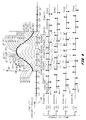
- the selected g(t) impulse response function is stored as array of binary numbers in ROM or RAM 71 which represent samples of the continuous g(t) impulse response function 91.
- the y-axis 93 represents both the magnitude and sign of the continuous g(t) function 91 and the magnitude and sign of samples of the g(t) function 91 which are stored as binary numbers in ROM or RAM 71 (indicated in Fig. 4 and 5 as discrete data points 105).
- the x-axis 95 represents time (t) and is divided into units of data clock intervals (T). One data impulse occurs per each data clock interval T 107. Each data clock interval is further subdivided into q equal size data clock subintervals 109 per data clock interval T.
- the parameter q may take on values 1,2,3,4 . . . data clock subintervals/data clock interval. As previously described, the parameter q also determines the "xq" data clock 77 rate.
- a binary number is stored in ROM or RAM 71 to represent the sampled value of the g(t) function for every data clock subinterval included in parameter L data clock intervals.
- the parameter L may take on values 1,2,3, . . . data clock intervals.
- the g(t) function may be symmetrically divided such that L*q/2 binary numbers are used to represent each of the upper and lower sides of the g(t) function relative to the maximum magnitude of the continuous g(t) function. Therefore, a total of L*q binary numbers which represent sampled values of the g(t) function are stored in ROM or RAM 71 for each two-level g(t) modulation format and 2*L*q binary numbers are stored for each four-level format. Outside +/- L/2 data clock intervals from the maximum, values of zero are assumed for g(t). The convolution algorithm does not operate on these zero values resulting in increased speed of execution.
- +/- L/2 +/- 3.5 data clock intervals from the maximum value of g(t) 91, the value of g(t) and the binary numbers representing samples of g(t) are set to equal zero. In Figs. 4 and 5, the maximum value of g(t) 91 occurs at 7.5 T.
- the first array of binary numbers represents the set of samples 105 of the g(t) function 91 just as for two-level modulation formats. This organization of this array is indicated in Table 3.
- the second array of binary numbers g′(t) 92 represents the set of samples 105 scaled by 1/3.
- Each array has individual values of L and q assumed for the respective stored array values. Also, it is possible to choose g′(t) values which are scaled by an amount other than 1/3. For example, all g′(t) array members may be defined to be zero, in which case the four-level modulation degenerates into three-level modulation.
- multiplications of stored binary numbers in ROM or RAM 71 which represent sampled g(t) values are not used in the convolution algorithm. Instead, additions or subtractions of the stored binary numbers in ROM or RAM 71 which represent either sampled g(t) values 105 or scaled samples of g(t) which are represented as g′(t) values 92 are used.
- addition and subtraction of sampled g(t) values 105 provide the identical result as multiplication by +1 or -1 since the converted input bimodal data impulses have values of +1 or -1.
- addition or subtraction of the sampled g(t) values which are scaled by 1/3 provide the same result as multiplication of g(t) sampled values times the converted bimodal data impulses having values of +1/3 and -1/3, respectively.
- Table 5 illustrates an example of the two-level modulation format convolution algorithm which operates on the g(t) impulse function samples 105 that are depicted in Fig. 4.
- the corresponding hardware block diagram is illustrated in Fig. 6.
- Table 6 illustrates the four-level modulation format convolution algorithm which operates on the g(t) and g′(t) impulse samples 105 and 92 respectively that are depicted in Fig. 5.
- the corresponding hardware block diagram is illustrated in Fig. 7.
- Tables 5 and 6 contain both the convolution process equations for the conventional convolution method using multiplication and accumulation, and the equivalent convolution method used in the present invention using additions and subtractions.
- D(m+n) indicates the value of a single bimodal data impulse function in the serial bimodal impulse data stream. Possible values for D(m+n) are +1 or -1 for two level modulation formats and +1, +1/3, -1/3, -1 for four level modulation formats.
- Parameter (m+n) is an index which represents the sequential position in time of each individual bimodal data impulse in the serial input data stream. Larger values of the index (m+n) indicate more recent data impulses.
- Parameter m is a reference index and parameter n is the sequential position of an individual bimodal data impulse relative to the reference index m.
- the process is then repeated for t6, t7, and t8.
- the data impulse stream index (m+n) is again incremented by one and the process is repeated again for t9, t10, t11 and t12. This process is repeated continuously.
- the process is then repeated for t6, t7, and t8.
- the data stream index (m+n) is again incremented by one and the process is repeated again for t9, t10, t11, and t12. This process is repeated continuously.
- the value of each data impulse function D(m+n) is indicated by an impulse symbol 111 on the D(m+n) versus time axes (97,99,101,103).
- Impulse symbols which point upward indicate positive values and impulse symbols which point downward indicate negative values.
- the length of each impulse symbol indicates its magnitude.
- the D(m+n) impulse data stream is sequentially moved to the right for each of the four convolution cycles by an amount which corresponds to one data clock subinterval 109.
- a dashed line connects each D(m+n) impulse 111 to a corresponding sampled g(t) or g′(t) array value 105, 92 which is added to or subtracted from the value in the Accum(t) 165 (as shown in Figs. 6 and 7) once during each convolution cycle. Addition is used when the value of D(m+n) is positive and subtraction is used when the value of D(m+n) is negative.
- the numerical values which represent samples of g(t) are multiplied by corresponding values of D(m+n) and subsequently added to the accumulation, Accum(t).
- the sign (+1 or -1) of each D(m+n) determines whether the numerical values which represent discrete values of the g(t) impulse response 105 or g′(t) scaled impulse response 92 are added to or subtracted from Accum(t).
- the absolute value (1 or 1/3) of D(m+n) determines whether numerical values used for the preceding addition or subtraction are addressed from the array which represents discrete values of g(t) 105 or from the array which represents discrete values of g′(t) 92.
- Fig. 6 illustrates a detailed block diagram of the premodulation filter 11 of Fig. 1 implementing the two-level modulation algorithm illustrated in Table 5 and Fig. 4.
- Fig. 7 illustrates a detailed block diagram of the premodulation filter 11 of Fig. 1 implementing the four-level modulation algorithm illustrated in Table 6 and Fig. 5.
- the array members for each modulation format are stored in ROM (or RAM) 155.
- the g(t) array members are loaded into RAM 155 via data bus 184.
- Ram 155 has enough capacity to store several g(t) arrays for different modulation types.
- Several types of continuous phase modulation digital modulation formats may be programmed on a computer (not shown) and corresponding g(t) arrays can be generated given the values of the parameters L and q.
- a user may also create his own g(t) arrays by whatever means he desires.
- the specific modulation format to be used is selected by a user by setting the associated array address on lines 182 for that portion of ROM (or RAM) 155 containing the g(t) array members corresponding to the desired modulation format.
- a g′(t) array must also be loaded into ROM (or RAM) 155 as well as a g(t) array.
- the premodulation filter characteristics may be changed very rapidly by switching between different g(t) arrays stored in ROM (or RAM) 155. If ROM is used, it must be loaded externally prior to assembly. In the preferred embodiment, RAM is utilized rather than ROM to allow not only switching between pre-loaded g(t) arrays, but also to allow dynamic loading of g(t) arrays and custom tailoring of g(t) arrays. Switching between g(t) arrays may be done by dynamic control of the array address lines 182 via controller 185 or by an external controller (not shown).
- a serial non-return-to-zero (NRZ) data stream is input on line 154.
- a data converter 158 converts the NRZ data stream to binary digits which represent a bimodal impulse stream.
- Logical 1's correspond to bimodal data impulses of value +1 and logical 0's correspond to bimodal data impulses of value -1.
- Shift register 162 is a 15 cell (bit) long one cell (bit) wide serial input, parallel output shift register which is clocked by the data clock on line 156.
- the NRZ input data stream present in shift register 162 is shifted one cell (corresponding to data clock period T) to the right and index (m+n) is incremented by one.
- the 15 parallel output lines 160 of shift register 162 are input to a multiplexer 161.
- Four address lines 157 from math state machine 153 control which of the 15 output lines 160 are selected to be on the +/- select line 164.
- the math state machine 153 is clocked by an asynchronous Int Clk on line 152 which operates at a much higher rate than the xq clock 159 and generates a portion of the ROM (or RAM) 155 address on lines 157 for each g(t) array element of the selected g(t) modulation format array.
- This portion of the ROM (or RAM) 155 address selects the particular data clock cell (T) from which g(t) array members are to be selected. For example, in Table 5 and Fig.
- NRZ data bit D(m+4) corresponds to g(t) members g(1), g(2), g(3) and g(4) during successive convolution subinterval periods t1, t2, t3 and t4, respectively, and are all selected by a single address on lines 157.
- address lines 157 are incremented to select g(t) members from ROM (or RAM) 155 and corresponding NRZ data bits from shift register 162.
- g(t) is divided into parameter L data clock intervals (maximum 15 due to 4 address lines) which corresponds to the maximum address which will be present on lines 157.
- the sample address state machine 151 is clocked by the xq clock 159 and generates another portion of the ROM (or RAM) 155 address on lines 150 for each g(t) array elements of the selected g(t) modulation format array.
- This portion of the ROM (or RAM) 155 address selects g(t) array members with the same relative position within each data clock cell T. For example, in Fig. 4, g(1), g(5), g(9), g(13), g(17), g(21) and g(25) are all selected with the same value on address lines 150.
- the maximum address which will present on lines 150 corresponds to q, which is the number of data clock subinterval periods/data clock period.
- the convolution algorithm follows the process previously described in Table 5.
- the initial value contained in Accum(t) is set by Initial Bias Value block 172. In the preferred embodiment, this is set to a value which corresponds to a value midway in the dynamic range of the accumulator 165.
- the accumulator 165 is set to this initial bias value preceding every convolution cycle via control from the Math State machine 153.
- the output of the accumulator 165 is coupled to latch 167 which is latched after every convolution cycle by the xq clock 159.
- the output of latch 167 is coupled to DAC 168 where it is converted to an analog signal smoothed by the analog reconstruction filter 169 to reduce spurious signals.
- the output of the analog reconstruction filter 169 on line 171 is coupled to the particular modulator 13 (shown in Fig. 1) being used in the system.
- An alternative to the analog output is the parallel digital output data bus 173 from the latch 167. This data bus is used in systems such as shown in Fig. 2 which require a digital input.
- the preferred embodiment uses 16 bit resolution in the convolution process with 12 bits being sent to latch 167 and the DAC 168.
- the reconstruction filter 169 reduces spurious frequency output from the DAC 168 due to digital quantization noise and sampling aliasing.
- the reconstruction filter 169 is a linear phase (constant group delay) analog filter having a selectable cutoff frequency over a wide range of data rates as dictated by the xq data clock 159 rate.
- Switches 178 and 179 will allow the apparatus in Fig. 7 to operate either in four-or two-level operation.
- switches 178 and 179 are in the two-level mode, the apparatus in Fig. 7 reduces to the apparatus in Fig. 6.
- a serial NRZ data stream is input to switch 178 and to a two-to-four bit coder 177 where pairs of serial input data bits are coded into two parallel bits on data lines 190 and 192.
- Data line 192 is the data input for shift register 162. Shift register 162 and multiplexer 161 operate as in two-level modulation operation where +/- control line 164 determines whether adder 163 adds or subtracts.
- Data line 190 is the data input for shift register 175 and multiplexer 173 which operate similarly to shift register 162 and multiplexer 161; control line 176 is an address line for ROM (or RAM) 155.
- Both g(t) and g′(t) arrays are stored in ROM (or RAM) 155.
- Address line 176 controls which array is addressed. Providing the remaining address lines 182, 150 and 157 remain constant, address line 176 will select g(t) or g′(t) array members corresponding to the same data clock subinterval, t1, t2, t3, etc.
- the first of the two serial logical input bits is embodied in data line 192.
- the logical level of data line 192 represents the sign of the binary number which represents the corresponding bimodal data impulse.
- the second of the two serial logical input data bits is embodied in data line 190.
- the logical level of data line 190 represents the magnitude of the binary number which represents the corresponding bimodal data impulse.
Landscapes
- Physics & Mathematics (AREA)
- Engineering & Computer Science (AREA)
- Computer Hardware Design (AREA)
- Mathematical Physics (AREA)
- Digital Transmission Methods That Use Modulated Carrier Waves (AREA)
Claims (8)
- Vorrichtung zum Erzeugen eines Modulationssignales zum Modulieren eines Trägersignales, mit einem programmierbaren digitalen Filter (163, 165, 167), der auf ein digitales Daten-Eingabesignal (154) anspricht und eine endliche Impuls-Response hat, die durch eine Responsefunktion (g(t)) definiert ist, welche die Impuls-Response entsprechend einem Modulationsformat darstellt, dadurch gekennzeichnet, daß der programmierbare digitale Filter (163, 165, 167) mit einer Speichereinrichtung (155) zum Speichern einer Vielzahl von Anordnungen von Filterkoeffizienten, wobei jede Anordnung eine unterschiedliche, wählbare Response-Funktion (g(t)) definiert, die einem unterschiedlichen, wählbaren Modulationsformat zugeordnet ist, und einer Steuereinrichtung (185), die mit dem programmierbaren digitalen Filter (163, 165, 167) und mit der Speichereinrichtung (155) gekoppelt ist, um eine gewünschte der Anordnungen von Filterkoeffizienten auszuwählen und um den programmierbaren digitalen Filter (165, 167, 169) so zu programmieren, daß er eine endliche Impuls-Response hat, die durch die Impuls-Response-Funktion (g(t)) entsprechend der gewünschten Anordnung definiert ist, gekoppelt ist.
- Vorrichtung nach Anspruch 1, dadurch gekennzeichnet, daß jede der Anordnungen von Filterkoeffizienten einen Satz numerischer Werte aufweist, die durch Berechnen der entsprechenden Response-Funktion (g(t)) an jedem einer Vielzahl von Probenpunkten bestimmt worden ist.
- Vorrichtung nach Anspruch 1 oder Anspruch 2, dadurch gekennzeichnet, daß Signalwandlermittel (158) so geschaltet sind, daß sie das digitale Daten-Eingabesignal (154) vor dem Empfang des Eingabesignales durch den programmierbaren digitalen Filter (163, 165, 167) auffangen, um das digitale Daten-Eingabesignal (154) in ein digitales Signal (97, 99, 101, 103) umzuwandeln, das eine Anzahl bimodaler Impulse mit positiven und negativen Amplituden darstellt.
- Vorrichtung nach einem der vorangehenden Ansprüche, dadurch gekennzeichnet, daß der programmierbare digitale Filter (163, 165, 167) eine Summiereinrichtung (163), die auf das digitale Signal (97, 99, 101, 103) anspricht, zum Aufsummieren der Filterkoeffizienten, die eine ausgewählte Response-Funktion (g(t)) definieren, wobei jeder der numerischen Werte einem diskreten Impuls entspricht, der durch das digitale Signal (97, 99, 101, 103) dargestellt wird und addiert wird, wenn der entsprechende Impuls eine positive Amplitude hat, und subtrahiert wird, wenn der entsprechende Impuls eine negative Amplitude hat; eine Akkumulatoreinrichtung (165), die mit der Summiereinrichtung (193) gekoppelt ist, um die Summe der numerischen Werte aufzurechnen, wobei die Akkumulatoreinrichtung (165) auf ein erstes Taktsignal (152) anspricht, um die Summe für jede erste Taktperiode zu aktualisieren; und eine Halteeinrichtung (167), die mit der Akkumulatoreinrichtung (165) gekoppelt ist und auf ein zweites Taktsignal (159) anspricht, um die Summe zwischenzuspeichern und sie jede zweite Taktperiode auszugeben, aufweist.
- Vorrichtung nach Anspruch 4, dadurch gekennzeichnet, daß weiterhin eine Schieberegistereinrichtung (162) mit einem seriellen Eingang, der mit der Signalwandeleinrichtung (158) zum Empfangen des digitalen Signales (97, 99, 101, 103) gekoppelt ist, einer Vielzahl paralleler Ausgänge (160) und einer Vielzahl von Speicherzellen, und die auf ein drittes Taktsignal (156) zum Verschieben des digitalen Signales (97, 99, 101, 103) anspricht, um eine Zelle bei jeder dritten Taktperiode zu verschieben, wobei jeder der parallelen Ausgänge (160) mit einer unterschiedlichen der Speicherzellen verbunden ist; und eine Multiplexereinrichtung (161), die mit der Vielzahl paralleler Ausgänge (160), mit der Steuereinrichtung (153, 185) und mit der Summiereinrichtung (163) verschaltet ist und die auf das erste Taktsignal anspricht, um das digitale Signal, das in jeder Speicherzelle vorliegt, jeweils eines zur Zeit, an die Summiereinrichtung (163) zu koppeln, vorgesehen ist, wobei das erste Taktsignal (152) eine Frequenz hat, die größer ist als die Frequenzen des zweiten und dritten Taktsignales (159; 156), und wobei die Frequenz des zweiten Taktsignales (159) größer ist als die Frequenz des dritten Taktsignales (156) und ein ganzzeiliges Vielfaches der Frequenz des dritten Taktsignales (156) ist.
- Vorrichtung gemäß einem der vorangehenden Ansprüche, dadurch gekennzeichnet, daß ein Digital-Analog-Wandler (168) an die Halteeinrichtung (167) zum Umwandeln der Summe in ein analoges Signal, das repräsentativ für das Modulationssignal ist, gekoppelt und ein Analogfilter (169) an den Digital-Analog-Wandler (168) zum Filtern des Analogsignals gekoppelt ist.
- Vorrichtung nach einem der vorangehenden Ansprüche, dadurch gekennzeichnet, daß die Speichereinrichtung (155) einen RAM mit dynamischer Eingangseinrichtung (184, 182) zum Echtzeitladen von Anordnungen von Filterkoeffizienten, die gewünschte Impulsfunktionen (g(t)) definieren, und zum dynamischen Neuprogrammieren der Summiereinrichtung (163, wobei die Steuereinrichtung (185) eine Einrichtung zum Modifizieren der Anordnungen von Filterkoeffizienten, die in dem RAM gespeichert sind, umfaßt.
- Vorrichtung nach einem der Ansprüche 4, 5, 6 oder 7, dadurch gekennzeichnet, daß Vorspannungsmittel (172) an die Kontrolleinrichtung (185) und an die Summiereinrichtung (163) zum Initialisieren der Inhalte der Akkumulatoreinrichtung (165) am Anfang jeder Periode des Datentaktsignales (156) gekoppelt sind.
Applications Claiming Priority (2)
| Application Number | Priority Date | Filing Date | Title |
|---|---|---|---|
| US104201 | 1979-12-17 | ||
| US07/104,201 US4757519A (en) | 1987-10-02 | 1987-10-02 | Digital premodulation filter |
Publications (3)
| Publication Number | Publication Date |
|---|---|
| EP0310457A2 EP0310457A2 (de) | 1989-04-05 |
| EP0310457A3 EP0310457A3 (en) | 1990-11-22 |
| EP0310457B1 true EP0310457B1 (de) | 1994-04-27 |
Family
ID=22299190
Family Applications (1)
| Application Number | Title | Priority Date | Filing Date |
|---|---|---|---|
| EP88309216A Expired - Lifetime EP0310457B1 (de) | 1987-10-02 | 1988-10-03 | Digitaler Vormodulationsfilter |
Country Status (5)
| Country | Link |
|---|---|
| US (1) | US4757519A (de) |
| EP (1) | EP0310457B1 (de) |
| JP (1) | JP2928522B2 (de) |
| CA (1) | CA1293778C (de) |
| DE (1) | DE3889276T2 (de) |
Families Citing this family (30)
| Publication number | Priority date | Publication date | Assignee | Title |
|---|---|---|---|---|
| NL8703084A (nl) * | 1987-12-21 | 1989-07-17 | Philips Nv | Digitaal premodulatiefilter. |
| US5051981A (en) * | 1988-01-21 | 1991-09-24 | Codex Corporation | Digital filtering |
| JP2518394B2 (ja) * | 1989-05-24 | 1996-07-24 | 日本電気株式会社 | エコ―キャンセラ方式全二重送受信回路 |
| US5140613A (en) * | 1990-05-25 | 1992-08-18 | Hewlett-Packard Company | Baseband modulation system with improved ROM-based digital filter |
| US5045817A (en) * | 1990-09-07 | 1991-09-03 | John Fluke Mfg. Co., Inc. | FM deviation control of direct digital synthesizers |
| DE4036512A1 (de) * | 1990-11-16 | 1992-05-21 | Philips Patentverwaltung | Digitale schaltungsanordnung zur naeherungsweisen realisierung einer gmsk (gaussian minimum shift keying)-modulation |
| DE4038903A1 (de) * | 1990-12-06 | 1992-06-11 | Telefunken Sendertechnik | Anordnung zur verarbeitung von signalen im modulationsweg zu einem sender |
| US5177769A (en) * | 1991-05-03 | 1993-01-05 | Bell Communications Research, Inc. | Digital circuits for generating signal sequences for linear TDMA systems |
| US5347542A (en) * | 1991-06-28 | 1994-09-13 | Motorola, Inc. | Demodulation selection for a communication signal |
| US5412691A (en) * | 1991-06-28 | 1995-05-02 | Digital Equipment Corporation | Method and apparatus for equalization for transmission over a band-limited channel |
| US5311556A (en) * | 1991-08-30 | 1994-05-10 | Elsag International B.V. | Digital FSK transmitter receiver and method of operating same |
| US5325400A (en) * | 1992-06-04 | 1994-06-28 | The Lan Guys, Inc. | Method and apparatus for predistortion of signals in digital transmission systems |
| US5657353A (en) * | 1992-12-31 | 1997-08-12 | Stellar One Corporation | Pulse shaping filter for received digital transmissions using phase lock loop for adjusting shift register |
| JPH06350654A (ja) * | 1993-06-14 | 1994-12-22 | Toshiba Corp | クロック同期制御検証装置 |
| KR100311072B1 (ko) * | 1993-08-31 | 2001-12-15 | 윤종용 | 다치중첩진폭변조의기저대역신호발생장치 |
| US5638405A (en) * | 1994-02-04 | 1997-06-10 | Amd | Dual-mode baseband controller for radio-frequency interfaces relating to digital cordless telephones |
| US5633893A (en) * | 1994-09-29 | 1997-05-27 | Ericsson Inc. | Digital modulation method with controlled envelope variation |
| US5644601A (en) * | 1994-10-31 | 1997-07-01 | Symbol Technologies, Inc. | Method and apparatus for bias suppression in a VCO based FM transmission system |
| US5768317A (en) * | 1995-05-08 | 1998-06-16 | National Semiconductor Corporation | Equalization filter compensating for distortion in a surface acoustic wave device |
| JPH11112581A (ja) * | 1997-10-06 | 1999-04-23 | Fujitsu Ltd | 変調システム |
| US5945885A (en) * | 1998-03-05 | 1999-08-31 | Hewlett-Packard Company | Digital baseband modulator adaptable to different modulation types |
| FR2776093A1 (fr) * | 1998-03-10 | 1999-09-17 | Philips Electronics Nv | Circuit processeur programmable muni d'une memoire reconfigurable, pour realiser un filtre numerique |
| US6281823B1 (en) * | 1999-09-21 | 2001-08-28 | Agere Systems Guardian Corp. | Direct digital synthesis using a sine weighted DAC |
| US20020199210A1 (en) * | 2001-06-26 | 2002-12-26 | Pingnan Shi | Universal test meter for digital signal distribution systems |
| US6999522B2 (en) * | 2001-09-28 | 2006-02-14 | Intersil Americas, Inc. | Constrained-envelope digital communications transmitter and method therefor |
| WO2003069867A1 (en) * | 2002-02-12 | 2003-08-21 | British Telecommunications Public Limited Company | Gaussian fsk modulation with more than two modulation states |
| US7248646B1 (en) * | 2002-04-19 | 2007-07-24 | Analog Devices Inc. | Digital reconfigurable core for multi-mode base-band transmitter |
| US7505537B1 (en) | 2003-03-25 | 2009-03-17 | Marvell International Ltd. | System and method for controlling gain and timing phase in a presence of a first least mean square filter using a second adaptive filter |
| US8779847B1 (en) | 2011-07-13 | 2014-07-15 | Marvell International Ltd. | Systems and methods for finite impulse response adaptation for gain and phase control |
| CN118590013B (zh) * | 2024-08-06 | 2024-12-03 | 中国科学技术大学 | 基于现场可编程门阵列的可调制射频信号的产生方法 |
Family Cites Families (12)
| Publication number | Priority date | Publication date | Assignee | Title |
|---|---|---|---|---|
| FR95978E (fr) * | 1967-10-07 | 1972-05-19 | Philips Nv | Dispositif pour la transmission d'impulsions synchrones. |
| GB1488433A (en) * | 1974-11-21 | 1977-10-12 | Ibm | Dpsk modulator |
| US3958191A (en) * | 1974-11-21 | 1976-05-18 | International Business Machines Corporation | Multi-line, multi-mode modulator using bandwidth reduction for digital fsk and dpsk modulation |
| US4003001A (en) * | 1974-11-21 | 1977-01-11 | International Business Machines Corporation | Multi-line, multi-mode modulator using bandwidth reduction for digital FSK and DPSK modulation |
| JPS5791058A (en) * | 1980-11-26 | 1982-06-07 | Toshiba Corp | Digital modulator |
| NL189588C (nl) * | 1981-04-01 | 1993-05-17 | Philips Nv | Zender voor hoekgemoduleerde signalen. |
| NL8201533A (nl) * | 1982-04-13 | 1983-11-01 | Philips Nv | Een zender ingericht voor het zenden van fm gemoduleerde signalen. |
| JPS59207720A (ja) * | 1983-05-11 | 1984-11-24 | Toshiba Corp | デジタルフイルタ |
| DE3333275A1 (de) * | 1983-09-15 | 1985-04-18 | ANT Nachrichtentechnik GmbH, 7150 Backnang | Uebertragungsanordnung fuer digitale signale |
| US4584540A (en) * | 1985-05-20 | 1986-04-22 | Rockwell International Corporation | Digital direct modulator with type of modulation selection |
| JPS62179211A (ja) * | 1986-02-03 | 1987-08-06 | Victor Co Of Japan Ltd | デジタル・グラフイツク・イコライザ |
| US4686490A (en) * | 1986-04-07 | 1987-08-11 | Hayes Microcomputer Products, Inc. | Digital data modulator and digital-to-analog converter |
-
1987
- 1987-10-02 US US07/104,201 patent/US4757519A/en not_active Expired - Lifetime
-
1988
- 1988-06-09 CA CA000569102A patent/CA1293778C/en not_active Expired - Lifetime
- 1988-09-30 JP JP63248889A patent/JP2928522B2/ja not_active Expired - Lifetime
- 1988-10-03 EP EP88309216A patent/EP0310457B1/de not_active Expired - Lifetime
- 1988-10-03 DE DE3889276T patent/DE3889276T2/de not_active Expired - Lifetime
Also Published As
| Publication number | Publication date |
|---|---|
| JP2928522B2 (ja) | 1999-08-03 |
| DE3889276D1 (de) | 1994-06-01 |
| DE3889276T2 (de) | 1994-11-17 |
| CA1293778C (en) | 1991-12-31 |
| EP0310457A2 (de) | 1989-04-05 |
| JPH01105647A (ja) | 1989-04-24 |
| EP0310457A3 (en) | 1990-11-22 |
| US4757519A (en) | 1988-07-12 |
Similar Documents
| Publication | Publication Date | Title |
|---|---|---|
| EP0310457B1 (de) | Digitaler Vormodulationsfilter | |
| EP0494696B1 (de) | Quadraturmodulationsschaltung | |
| EP0169612B1 (de) | Auf Datensignale ansprechende Vorrichtung zur Erregung eines winkelmodulierten Trägersignals konstanter Amplitude | |
| US5812608A (en) | Method and circuit arrangement for processing received signal | |
| EP0716785B1 (de) | Verbessertes rom filter | |
| US5590155A (en) | Equipment for generating a transmit signal from first and second digital signals | |
| EP0440187B1 (de) | Einrichtung zur Umwandlung eines binären Eingangssignals in entsprechende Quadratursignale | |
| JPH1023096A (ja) | ディジタル変調器および復調器 | |
| KR19980087508A (ko) | 고정된 샘플링 속도를 사용한 이산시간 샘플시스템들을 위한 가변속도 다운샘플링 필터 장치 및 그 방법 | |
| JPH06188927A (ja) | ディジタル信号の送信方法及びそのための送信器 | |
| US6944250B2 (en) | Variable rate modulator | |
| US4812786A (en) | Method and system for providing precise multi-function modulation | |
| JPH0683277B2 (ja) | 角度変調信号発生回路及びそれに関連する振幅及び位相変調信号発生回路 | |
| US7046738B1 (en) | 8-PSK transmit filtering using reduced look up tables | |
| US7158578B2 (en) | Quadrature modulator with pulse-shaping | |
| US7450659B2 (en) | Digital modulator employing a polyphase up-converter structure | |
| US5872532A (en) | Selection apparatus | |
| JP3147000B2 (ja) | 疑似gmsk変調装置 | |
| US5581253A (en) | Implementation and method for a digital sigma-delta modulator | |
| US5198779A (en) | Digital oscillator | |
| US5495504A (en) | Signal generating apparatus | |
| US6194977B1 (en) | State variable-based table-driven modulation signal generation | |
| EP0704978B1 (de) | Auswahlvorrichtung zur Wahl elektrischer Zellen und Gerät zur Anwendung einer solchen Vorrichtung | |
| EP0620667A1 (de) | Modulator für pi/4 QPSK Signale | |
| JPH06104943A (ja) | 四相位相変調装置 |
Legal Events
| Date | Code | Title | Description |
|---|---|---|---|
| PUAI | Public reference made under article 153(3) epc to a published international application that has entered the european phase |
Free format text: ORIGINAL CODE: 0009012 |
|
| AK | Designated contracting states |
Kind code of ref document: A2 Designated state(s): DE FR GB IT |
|
| PUAL | Search report despatched |
Free format text: ORIGINAL CODE: 0009013 |
|
| AK | Designated contracting states |
Kind code of ref document: A3 Designated state(s): DE FR GB IT |
|
| 17P | Request for examination filed |
Effective date: 19910405 |
|
| 17Q | First examination report despatched |
Effective date: 19930730 |
|
| GRAA | (expected) grant |
Free format text: ORIGINAL CODE: 0009210 |
|
| AK | Designated contracting states |
Kind code of ref document: B1 Designated state(s): DE FR GB IT |
|
| ITF | It: translation for a ep patent filed | ||
| REF | Corresponds to: |
Ref document number: 3889276 Country of ref document: DE Date of ref document: 19940601 |
|
| ET | Fr: translation filed | ||
| PLBE | No opposition filed within time limit |
Free format text: ORIGINAL CODE: 0009261 |
|
| STAA | Information on the status of an ep patent application or granted ep patent |
Free format text: STATUS: NO OPPOSITION FILED WITHIN TIME LIMIT |
|
| 26N | No opposition filed | ||
| REG | Reference to a national code |
Ref country code: GB Ref legal event code: 732E |
|
| REG | Reference to a national code |
Ref country code: GB Ref legal event code: 732E |
|
| REG | Reference to a national code |
Ref country code: FR Ref legal event code: TP |
|
| REG | Reference to a national code |
Ref country code: FR Ref legal event code: TP |
|
| REG | Reference to a national code |
Ref country code: GB Ref legal event code: IF02 |
|
| PG25 | Lapsed in a contracting state [announced via postgrant information from national office to epo] |
Ref country code: IT Free format text: LAPSE BECAUSE OF NON-PAYMENT OF DUE FEES;WARNING: LAPSES OF ITALIAN PATENTS WITH EFFECTIVE DATE BEFORE 2007 MAY HAVE OCCURRED AT ANY TIME BEFORE 2007. THE CORRECT EFFECTIVE DATE MAY BE DIFFERENT FROM THE ONE RECORDED. Effective date: 20051003 |
|
| PGFP | Annual fee paid to national office [announced via postgrant information from national office to epo] |
Ref country code: GB Payment date: 20061025 Year of fee payment: 19 |
|
| PGFP | Annual fee paid to national office [announced via postgrant information from national office to epo] |
Ref country code: DE Payment date: 20071130 Year of fee payment: 20 |
|
| GBPC | Gb: european patent ceased through non-payment of renewal fee |
Effective date: 20071003 |
|
| REG | Reference to a national code |
Ref country code: FR Ref legal event code: ST Effective date: 20080630 |
|
| PGFP | Annual fee paid to national office [announced via postgrant information from national office to epo] |
Ref country code: FR Payment date: 20061017 Year of fee payment: 19 |
|
| PG25 | Lapsed in a contracting state [announced via postgrant information from national office to epo] |
Ref country code: GB Free format text: LAPSE BECAUSE OF NON-PAYMENT OF DUE FEES Effective date: 20071003 |
|
| PG25 | Lapsed in a contracting state [announced via postgrant information from national office to epo] |
Ref country code: FR Free format text: LAPSE BECAUSE OF NON-PAYMENT OF DUE FEES Effective date: 20071031 |