EP0310655B1 - Kontinuierlich bereitgestellter impulszugprozessor hoher zuverlässigkeit - Google Patents
Kontinuierlich bereitgestellter impulszugprozessor hoher zuverlässigkeit Download PDFInfo
- Publication number
- EP0310655B1 EP0310655B1 EP88904099A EP88904099A EP0310655B1 EP 0310655 B1 EP0310655 B1 EP 0310655B1 EP 88904099 A EP88904099 A EP 88904099A EP 88904099 A EP88904099 A EP 88904099A EP 0310655 B1 EP0310655 B1 EP 0310655B1
- Authority
- EP
- European Patent Office
- Prior art keywords
- pulse
- module
- pulses
- train
- pulse train
- Prior art date
- Legal status (The legal status is an assumption and is not a legal conclusion. Google has not performed a legal analysis and makes no representation as to the accuracy of the status listed.)
- Expired - Lifetime
Links
Images


Classifications
-
- G—PHYSICS
- G08—SIGNALLING
- G08B—SIGNALLING SYSTEMS, e.g. PERSONAL CALLING SYSTEMS; ORDER TELEGRAPHS; ALARM SYSTEMS
- G08B13/00—Burglar, theft or intruder alarms
- G08B13/22—Electrical actuation
- G08B13/24—Electrical actuation by interference with electromagnetic field distribution
- G08B13/2402—Electronic Article Surveillance [EAS], i.e. systems using tags for detecting removal of a tagged item from a secure area, e.g. tags for detecting shoplifting
- G08B13/2465—Aspects related to the EAS system, e.g. system components other than tags
- G08B13/2488—Timing issues, e.g. synchronising measures to avoid signal collision, with multiple emitters or a single emitter and receiver
-
- G—PHYSICS
- G08—SIGNALLING
- G08B—SIGNALLING SYSTEMS, e.g. PERSONAL CALLING SYSTEMS; ORDER TELEGRAPHS; ALARM SYSTEMS
- G08B13/00—Burglar, theft or intruder alarms
- G08B13/22—Electrical actuation
- G08B13/24—Electrical actuation by interference with electromagnetic field distribution
- G08B13/2402—Electronic Article Surveillance [EAS], i.e. systems using tags for detecting removal of a tagged item from a secure area, e.g. tags for detecting shoplifting
- G08B13/2465—Aspects related to the EAS system, e.g. system components other than tags
- G08B13/2468—Antenna in system and the related signal processing
- G08B13/2471—Antenna signal processing by receiver or emitter
Definitions
- the present invention is directed to the field of noise rejection circuitry, and more particularly, to a continuously armed, highly reliable, pulse train processor especially for magnetic strip and resonant tag signal detection.
- Magnetic and swept frequency systems, components and subsystems are disclosed in United States Patents No's. 3,810,147, 3,828,337, 3,863,244, 3,913,219, 3,938,044, 3,961,322, 3,967,161, 4,021,705, 4,117,466, 4,168,496, 4,243,980, 4,251,808, 4,260,990, 4,498,076, 4,567,473, and in Canadian Patent No. 1005546, of the same inventive entity as herein, each being incorporated herein by reference.
- United States Patent 3,961,322 discloses receiver circuitry operative to distinguish an interrogation signal in the form of an interrogation signal pulse train from environmental and other spurious signals.
- the therein disclosed receiver circuitry In response to the pulse height of the initial pulse of the received pulse train, the therein disclosed receiver circuitry starts a counter.
- the counter with each increment enables a sequential pulse descrimination module until it cycles through a predetermined time sequence that sequentially enables all of the pulse descrimination modules.
- the prior system cannot be reset until after the entire cycle has been gone through, so that during this whole time, the prior system is locked-up, and is subjected to an undesireable failure of alarm situation.
- each pulse discrimination module of the prior system is limited with respect to the capability that it is able to discriminate the characteristics of the pulses, such that if the pulses meet predetermined merely minimum duration conditions, the disclosed receiver circuitry produces an alarm, notwithstanding that the pulses may later exhibit totally unexpected characteristics typically representative of noise, so that the prior system is thereby subjected to an undesireable false alarm situation.
- United States patent publication 3,863,244 discloses a device as cited in the preamble of claim 1.
- the publication discloses receiver circuitry capable of distinguishing true resonant signals from noise and other spurious signals.
- This publication similarly provides pulsed discrimination which is capable of discriminating with respect to a minimum duration condition only, failing to provide noise rejection circuitry capable of detecting received pulses having a duration greater than that expected.
- this known system is operative for discriminating between the rate at which the frequency of a received signal changes to ascertain whether the signal is caused by a tag circuit or by noise conditions, received pulses which pass these limited criteria may also exhibit characteristics representative of spurious signals, and a system according to this publication may allow such spurious signals to be processed, resulting in false alarms.
- the present invention contemplates as one of its objects the provision of a pulse train processor capable of processing the several constitutive consecutive pulses of a magnetic system pulse train in such a way that the processing occurs without locking-up the system after processing of an initial pulse is initiated so that the system is substantially continuously armed.
- the present invention accomplishes this object by providing a pulse train processor operative to discriminate the constitutive pulses of the received pulse train with respect to whether they severally satisfy certain expected characteristics in such a way that if any of the pulses fails to satisfy its corresponding expected characteristics, the processor resets itself immediately, without having to first complete any timing cycle.
- the present invention contemplates as another object a pulse train processor that discriminates the several constitutive pulses with respect to both minimum as well as maximum conditions, and that provides an output alarm if the pulses severally satisfy the minimum conditions and only if they do not exceed the maximum conditions whereby a high reliability of output alarm signaling is substantially ensured.
- the present invention accomplishes this object by providing a pulse train processor that is responsive to both the minimum duration and to the maximum duration of each of the several pulses, and alarms if and only if each of the pulses is within its respective minimum and maximum bounds and the several pulses occur in their proper time sequence.
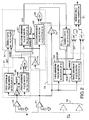
- FIG. 10 generally designated at 10 is a block diagram of the continuously armed, high reliability pulse train processor in an exemplary magnetic and resonant interrogation system receiver application according to the present invention.
- the present invention has its utility in discriminating true signal from noise in a field disturbance responsive receiver sensitive to the movement of a marked tag through an interrogation zone to provide an alarm representative of shoplifting and other unlawful taking in retail stores, libraries and the like.
- a transmitter generally designated 12 drives an antenna 14 which generates either a low-frequency or a radio frequency magnetic field in a specific area called the "interrogation zone".
- a second and separate antenna 15 connected to a receiver generally designated 16 is responsive to changes in the magnetic field caused by a so-called target 18 schematically illustrated by a circle with a "X" therethrough.
- the target is typically a high permeability magnetic strip which saturates abruptly as compared to the period of the changing magnetic field.
- the interrogation signal consists of a radio frequency signal which is frequency modulated approximately five to ten percent of the center frequency.
- the target is a resonant circuit tuned to be near the center frequency of the interrogation signal. Each time that the frequency of the interrogation signal passes through the resonant frequency of the target, an abrupt change takes place in the magnetic field.
- the signal induced by the abrupt change in the magnetic field is sensed by the receiver antenna 15, is demodulated by the receiver 16, filtered in a band-pass filter 20 to remove noise, and amplified in an amplifier 22. Thereafter, the signal is fed in parallel into the pulse train processor 24 to be described of the present invention.
- the pulse train processor 24 is operative to distinguish true target signals from noise, and in such a way as to be both substantially continuously armed and to provide a very high confidence detection signal.
- the pulse train processor is operative to produce an output trigger pulse if each of the pulses of the pulse train have a height above a predetermined threshold that severally exist during selected but precisely defined time windows and only if the several pulses occur in a predetermined polarity sequence.
- a first necessary but not sufficient criteria that must be satisfied if the processor 24 is to produce an output trigger pulse representative of a true signal is that the received pulses as produced by the tag being in the interrogation zone or otherwise arising must correspond to an expected polarity sequence of an ideal pulse train.
- such an expected polarity sequence is, on the one hand, a succession of a positive a negative and a positive pulse, and on the other hand, a succession of a negative a positive and a negative pulse.
- the pulse train processor 24 does not produce the output trigger pulse if the received pulse train does not conform to the expected polarity sequence.
- the pulse train processor includes a plurality of pulse processing modules each dedicated to corresponding ones of the expected pulses of the ideal pulse train.
- a plurality of pulse processing modules each dedicated to corresponding ones of the expected pulses of the ideal pulse train.
- three pulse processing modules 26, 28, and 30 are disclosed, although a different number of pulse processing modules are possible in accordance with the number of pulses expected to be produced in the particular control system, one pulse processing module being dedicated to the expected characteristics of each of the several pulses of the ideal pulse train.
- the several modules 26, 28, 30 are respectively dedicated to the constitutive pulses of the exemplary tertiary pulse ideal pulse train.
- each of the received pulses must meet predetermined minimum, maximum, and threshold criteria if the pulse train processor is to produce an output trigger pulse.
- Each module 26, 28, 30 is operative to detect whether the corresponding pulse exceeds a predetermined pulse height threshold for a time longer than a predetermined first time but not longer than a predetermined second time. But if the corresponding pulse processing modules are not satisfied that the corresponding pulses conform to these very accurate several criteria, the pulse train processor rejects the received pulses as spurious, and false alarms are thereby substantially prevented.
- the pulse train processor is substantially continuously armed, and no timers or other sequencing devices lock out system responsiveness. If the characteristics of the first received pulse of the pulse train correspond to the expected characteristics thereof, the module 26 is operative to enable the module 28. But if the characteristics of that pulse do not correspond do the expected characteristics of the pulse, the module 26 does not enable but rather resets the module 28, and the processor is therewith returned to its armed state.
- the module 26, in the preferred embodiment, is always enabled.
- the module 28, assuming it was enabled by the upstream module 26, is operative to determine whether the next pulse of the received pulse train has characteristics that correspond to the expected characteristics associated with that pulse in the ideal pulse train. In the event that the pulse does have the requisite pulse characteristics, the pulse module 28 enables the downstream pulse detection module 30.
- each module is self-resetting at the termination of the corresponding pulse, as described more fully below.
- the module 30 If the several modules 26, 28, 30 detect the expected characteristics of the corresponding pulses of the pulse train in the correct temporal polarity sequence, the module 30 provides an output trigger pulse signaling detection of a pulse train representative of a tag being present in the interrogation zone.
- a monostable multivibrator 32 is connected to the output module of the pulse train processor 24.
- the monostable multivibrator 32 produces a pulse in response to each trigger signal out of the the pulse train processor.
- the monostable multivibrator 32 may be part of a missing pulse detector described in U.S. Patent 3,828,337 of the same inventive entity as herein, incorporated herein by reference.
- An integrating and threshold circuit 34 to be described is connected to the output of the multivibrator 32.
- the processor 50 includes three pulse processing modules illustrated in dashed outline 52, 54, and 56.
- the modules 52, 54, 56 are dedicated to a positive pulse, a negative pulse and a positive pulse defining an expected pulse train sequence.
- the positive, negative, positive pulse three pulse pulse train is exemplary only.
- another bank of pulse processing modules not specifically illustrated, may be employed for a three pulse pulse train having a negative, positive, and a negative pulse polarity sequence.
- the principles of the instant invention can be employed with other numbers of constitutive pulses of an expedited pulse train with a different expected polarity sequence without departing from the inventive concept.
- a positive threshold detector 59 and a negative threshold detector 61 are connected in parallel to receive the filtered and amplified signal of the receiver of the magnetic interrogation system.
- the modules 52, 54, and 56 are so connected to corresponding thresholds that the modules dedicated to positive pulses are connected to the positive threshold detector 59 while the module dedicated to the negative pulse is connected to the negative threshold detector 61.
- the modules are severally responsive to the output of the threshold detectors 59, 61 to enable as well as disable the succeeding stages in dependence on whether or not the pulse corresponding to the prior stage module is within its expected bounds. The modules reset themselves whenever the corresponding pulse for that module passes away.
- Each of the modules 52, 54, 56 includes a minimum pulse width detector 60, 62, 64 and a maximum pulse width detector 66, 68, and 70 connected to receive the output of the corresponding positive or negative threshold detector 59, 61.
- the minimum and maximum pulse width detector pairs 60, 66; 62, 68; and 64, 70 of the modules 52, 54, and 56 respectively are selected to conform to the expected duration time and magnitude characteristics of the corresponding constitutive pulses of the expected pulse train. Only the correct polarity sequence of pulses above a preselected threshold that exist within carefully defined time durational windows are passed through by the pulse train processor, while all other pulse signal kinds and types are rejected thereby as undesirable noise.
- Inverters 72, 74, and 76 are respectively connected to the output of the positive threshold detector 59, the output of the negative threshold detector 61, and the output of the positive threshold detector 59.
- the output of the inverters 72, 74 and 76 are respectively connected to the reset inputs of the minimum and maximum pulse-width detector pairs 60, 66; 62, 68; and 64, 70 of the pulse processing modules 52, 54, and 64.
- the inverters are respectively responsive to the falling edge of the pulse output of the corresponding threshold detectors 59, 61 for resetting, at the trailing edge of each pulse, the pulse processing module associated with the respective inverters.
- the several pulse processing modules, insofar as the minimum and maximum pulse-width detectors associated therewith are reset by the trailing edge of the pulses analysed thereby, are substantially continuously armed.
- An enable gate 78 is connected between the output of the minimum pulse-width detector 60 of the initial pulse processing module 52 and the enable input of both of the minimum and of the maximum pulse-width detectors 62, 68 of the downstream pulse processing module 54.
- An enable gate 80 is connected to the output of the minimum pulse-width detector 62 of the pulse processing module 54 and the enable input of both the minimum and the maximum pulse-width detectors 64, 70 of the pulse processing module 56.
- the gates 78, 80 are toggled to logic "1" provided the pulses analysed in the modules 52, 54 satisfy preselected minimum duration conditions.
- the gates 78, 80 enable the downstream modules 54, 56, and in such a way that the initial module enables the intermediate module 54, and thereafter the intermediate module enables the downstream module 56, and so on time sequentially, in dependence on receiving a pulse train having the proper pulse polarity sequence the constitutive pulses of which having the proper minimum durations.
- the minimum pulse-width detector 60 of the initial module 52 is always enabled, and is responsive to detection of a positive pulse beyond the threshold established by the threshold detector 59 that subsists for at least a specified minimum time to set the enable gate 78.
- the enable gate 78 is driven to the logic "1" state thereby, and enables the detectors 62, 68 of the intermediate module 54. If a negative polarity pulse of the requisite height is received in immediate temporal sequence, the detectors 62, 68, already in the enabled condition, are thereby able to respond to the duration of the negative pulse of the pulse train. If the negative polarity pulse is timely and is of a duration that matches the minimum duration expected for that pulse, the minimum pulse width detector 62 of the module 54 sets the enable gate 80.
- the gate 80 is driven to the logical "1" state, which in turn enables the detectors 64, 70 of the module 56. If a positive polarity pulse is then received of at least the threshold expected by the positive threshold detector 59, the minimum pulse-width detector 64, already in the enabled condition is able to determine whether or not it satisfies the minimum duration condition expected for that pulse. If it does, a trigger signal is output therefrom to the monostable multivibrator 81 via an OR gate 82. The OR gate 82 also receives the trigger output signal from the terminal module of the "negative, positive, negative" pulse train processor 58.
- One input of an OR gate 84 is connected to the output of the inverter 74, and another input of the OR gate 84 is connected to the output of the maximum pulse-width detector 66 of the processing module 52.
- the output of the OR gate 84 is connected in parallel to the reset input of the enable gate 78 and to the reset inputs of the minimum and of the maximum pulse-width detectors 62, 68 of the pulse processing module 54.
- One input of an OR gate 86 is connected to the output of the inverter 76, and another input thereof is connected to the output of the maximum pulse-width detector 68 of the module 54.
- the output of the OR gate 86 is connected in parallel to the reset input of the enable gate 80 and to the reset inputs of the minimum and maximum pulse width detectors 64, 70 of the pulse processing module 56.
- the OR gates 84, 86 are operative, on the one hand, to pass through the output pulses of the associated inverters to reset the detectors 62, 68 and the detectors 64, 70 of the modules 54, 56 after the perishing of the corresponding pulse.
- the OR gates 84, 86 are further responsive to the same condition, that is to the occurrence of the trailing edge of the corresponding pulse, to reset the enable gate 78, and the enable gate 80.
- the gates 78, 80 are thereby toggled to the binary "0" state, and must await the occurance of the appropriate duration and polarity pulse.
- the OR gates 84, 86 are responsive to an output from the maximum pulse-width detector 66 and to an output from the maximum pulse-width detector 68 of the modules 52, 54 for resetting the enable gate 78 and minimum and maximum detectors 62, 68 of the module 54, and for resetting the enable gate 80 and the minimum and maximum detectors 64, 70 of the module 56.
- the detectors of the several modules as well as their associated enabling gates are thereby reset in the event that the pulse associated with the corresponding upstream module endures for a time period longer than the expected time period.
- figure 3 generally designated at 100 in figure 3-A thereof is a graph illustrating a typical "tag" signal for an exemplary resonant tuned circuit system consisting of a pulse train having a positive polarity, a negative polarity, and a positive polarity pulse.
- a curve generally designated 102 in figure 3-B illustrates the positive pulses having the widths designated "W-1", "W-3" produced by the positive threshold detector 59 (figure 2) as the pulse train 100 is delivered thereto.
- the leading and trailing edges defining the widths of the pulses are delimited respectively at the times when the positive pulses of the pulse train exceed and fall below the preselected threshold as selectably provided therefor by the positive threshold detector.
- a pulse having a width designated "W-2" is provided by the negative threshold detector 61 (figure 2), and in such a way that the duration thereof is delimited by the negative threshold level selected for the negative threshold detector.
- pulses are produced at the trailing edge of the pulses illustrated by the graph 102 in figure 3-B by the inverters 74, 76 (figure 2) coupled to receive the output signal of the positive threshold detector, and as shown by a graph 108 in figure 3-E, a pulse is produced at the trailing edge of the output signal of the negative threshold detector 62 (figure 2) as the corresponding pulse falls below the preselected threshold.
- pulses are produced by the pulse-width detector 60 (figure 2) of the initial pulse processing module 52 (figure 2) as soon as the duration of the pulse corresponding thereto exceeds the minimum duration selected for that pulse processing module.
- the minimum duration is designated as "tau1" in figure 3-F.
- the third pulse of the pulse train illustrated in figure 3-A likewise produces a pulse out of the minimum pulse detector 52, (figure 2) as the pulse train is fed to the several modules in parallel.
- a pulse is produced by the maximum pulse-width detector 66 of the module 52 (figure 2) upon the pulse exceeding the maximum duration conditions prescribed for the pulse corresponding to the first pulse processing module. As appears below, the output of the maximum pulse-width detector resets the downstream module, thereby preventing a false alarm.
- the gate 78 (figure 2) is toggled to the logical "1" state with the rising edge of the first pulse illustrated in the graph 110 of figure 3-F.
- the gate signal is toggled to the logical "0" condition upon the occurance of the leading edge of the negative pulse signal illustrated by the graph 108 in figure 3-E.
- the enable gate 78 (figure 2) as illustrated by the second pulse of the graph 114 is toggled to the logical "1" state upon the leading edge of the second pulse of the graph 110 in figure 3-F representative of the third pulse of the pulse chain exceeding the minimum condition for duration prescribed for the first pulse.
- the gate is toggled to the logical "0" state by the leading edge of the output pulse of the maximum pulse-width detector illustrated by the graph 112 in figure 3-G.
- the enable gate 78 (figure 2) is reset by the output of the OR gate 84, (figure 2) which output is produced either by the termination of the negative pulse, represented by the first pulse of the graph 116, or by the timing out of the maximum pulse-width detector 66 of the module 52, (figure 3).
- the minimum detector 62 of the module 54 produces a pulse after a specified minimum time duration after the beginning of the pulse produced by the negative threshold detector as can be seen by comparing the graph 104 of figure 3-C.
- the maximum pulse-width detector of the intermediate module provides an output pulse after a preselected time interval designated "tau4" from the beginning of the pulse produced by the negative threshold detector.
- the enable gate of the third and final processing module in the illustrated embodiment is toggled to the logical "1" state in response to the occurence of the output pulse of the upstream minimum pulse-width detector, as best seen by comparing graph 118 of figure 3-J.
- the enable gate for the terminal module is toggled to the logical "0" state in response to the trailing edge of the third constitutive pulse of the pulse train as can be seen by comparing the second pulse of the graph 102 of figure 3-B.
- the reset for the enable gate is illustrated by the graph generally designated 124 in figure 3-M.
- the minimum pulse-width detector of the terminal module of the pulse train processor produces a pulse upon the corresponding pulse of the pulse train satisfying a duration condition designated "tau5" specified therefor.
- the maximum pulse-width detector of the third processing module provides a pulse at a time when the corresponding pulse of the pulse train subsists for a time as long as the maximum time specified for that pulse and designated by an interval "tau6".
- the pulse is illustrated in dashed outline for reasons that appear immediately below.
- the minimum pulse-width signal represented as the pulse in the graph 126 of Figure 3-N triggers the monostable multivibrator 81 (figure 1).
- the monostable multivibrator is retriggerable, and would be retriggered in the event that the pulse persists for a time longer than the prescribed time. In that event, the multivibrator would be reset, and a failure of alarm condition would thereby be prevented.
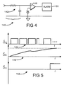
- FIG. 140 generally designated at 140 is a schematic circuit diagram illustrating the integration and averaging circuit of the present invention.
- the pulse output stream provided by the retriggerable monostable multivibrator is integrated in an R, C network generally designated 142.
- the input signal applied to the integrator 142 is the output of the monostable multivibrator.
- the output pulses are integrated by the integrator 142 producing a potential that rises with each pulse output of the monostable multivibrator as shown by a graph generally designated 146 in Figure 5-B.
- the integrated signal is applied to a threshold comparator 148.
- the comparator provides an output signal to an alarm 150 if the magnitude of the integrated signal potential exceeds the selected threshold of the comparator 148 as illustrated by the dashed line in figure 5-B, and, thereafter, an alarm is signaled by a graph generally designated 152 in figure 5-C.
Landscapes
- Engineering & Computer Science (AREA)
- Physics & Mathematics (AREA)
- Automation & Control Theory (AREA)
- Computer Security & Cryptography (AREA)
- Electromagnetism (AREA)
- General Physics & Mathematics (AREA)
- Signal Processing (AREA)
- Burglar Alarm Systems (AREA)
- Air Bags (AREA)
- Time-Division Multiplex Systems (AREA)
Claims (25)
- Impulsfolgeprozessor (10; 50) für einen Feldstörsensor, mit
Mitteln (15, 16, 20, 22) zum Vorsehen einer Impulsfolge von konstitutiven, aufeinanderfolgenden Impulsen als Reaktion auf eine magnetische Kennzeichnung (18), die sich in einem Abfragebereich des Feldstörsensors befindet,
gekennzeichnet durch
zurücksetzbare Mittel (25), die mit der Impulsfolge gekoppelt sind und Mittel zum aufeinanderfolgenden Bestimmen vorsehen, ob die mehreren konstitutiven Impulse seriell mit vorbestimmten minimalen und maximalen temporären Dauerkriterien übereinstimmen, welche dafür eingerichtet wurden, und
Mittel, welche mit den zurücksetzbaren Mitteln (24) zusammenwirken und auf einen Fehler irgendeines Impulses der Impulsfolge reagieren, um den entsprechenden Kriterien zum Zurücksetzen der zurücksetzbaren Mittel (24) derart zu genügen, daß die zurücksetzbaren Mittel (24) wiederum in die Lage gesetzt werden, aufeinanderfolgend nach der Initialisierung zu bestimmen, ob aufeinanderfolgend empfangene Impulse der Impulsfolge, welche seriell nach dem Zurücksetzen der zurücksetzbaren Mittel (24) empfangen wurden, den dafür eingerichteten Impulsfolgekriterien ensprechen, d.h., daß der Impulsfolgeprozessor (10; 50) fortlaufend betriebsbereit ist,
wobei die zurücksetzbaren Mittel (24) ein Feld von aktivierbaren Impulsverarbeitungsmodulmitteln (26, 28, 30; 52, 54, 56) enthalten, die die Impulsfolge empfangen, wobei wiederum die Modulmittel zum Erfassen der erwarteten Minimal- und Maximaldauerkriterien eines unterschiedlichen konstitutiven Impulses der Impulsfolge vorgesehen sind, und
wobei die zurücksetzbaren Mittel (24) aktivierbare Gatter (78, 80) enthalten, die seriell zwischen die ersten und letzten der Pulsverarbeitsmodulmittel (26, 28, 30; 52, 54, 56) geschaltet sind, zum Definieren von stromauf- und stromabliegenden Pulsverarbeitungsmodulmitteln, die Gatter (78, 80) sind zum Aktivieren der stromabliegenden Modulmittel betätigbar, wenn und nur in Reaktion auf eine Erfassung der stromaufliegenden Modulmittel der entsprechenden, vorbestimmten Impulskriterien, die Gatter (78, 80) sind ferner für ein Reaktivieren der stromabliegenden Modulmittel derart betätigbar, sowohl in Reaktion auf die Beendigung des Impulses entsprechend den Modulmitteln als auch in Reaktion auf die Erfassung der stromaufliegenden Modulmittel, daß die Impulscharakteristika, die diesem Impuls entsprechen, die Maximaldauerkriterien, wie vorstehend beschrieben, überschreiten. - Impulsfolgeprozessor nach Anspruch 1, indem die Gatter Flipflops sind, welche wählbare logische Zustände aufweisen, wobei die Flipflops die Aktivierung der stromabliegenden Modulmittel und die Deaktivierung derselben entsprechend den logischen Zuständen der Flipflops verursachen.
- Impulsfolgeprozessor nach Anspruch 1, in dem die temporären Minimal- und Maximaldauerkriterien mit zugewiesenen Pulsweitendetektoren angewendet werden.
- Durchgehend betriebsbereiter Impulsfolgeprozessor für einen Sensor einer gewobbelten Funkfrequenz, mit
Mitteln zum Vorsehen einer Impulsfolge von konstitutiven fortlaufenden Impulsen in Reaktion auf eine Resonanzkennzeichnung, welche in einem Abfragebereich eines Sensors für eine gewobbelte Funkfrequenz vorhanden ist,
zurücksetzbaren Mitteln, die mit den die Impulsfolge vorsehenden Mitteln verbunden sind, zum sequentiellen Bestimmen, ob die verschiedenen konstitutiven Impulse seriell vorbestimmte und temporäre Minimal- und Maximaldauerkriterien erfüllen, welche dafür eingerichtet sind, und
Mitteln, die mit den zurücksetzbaren Mitteln zusammenwirken und auf einen Fehler von irgendeinem Impuls der Impulsfolge reagieren, zum Erfüllen der entsprechenden Kriterien für ein Zurücksetzen der zurücksetzbaren Mittel derart, daß die zurücksetzbaren Mittel wiederum für ein sequentielles Bestimmen nach Initialisierung in der Lage sind, ob die sequentiell empfangenen Impulsfolgepulse, welche seriell nach dem Zurücksetzen der zurücksetzbaren Mitteln empfangen wurden, die dafür eingerichteten vorbestimmten Impulsfolgekriterien erfüllen. - Impulsfolgeprozessor nach Anspruch 4, indem die zurücksetzbaren Mittel ein Feld von aktivierbaren Impulsverarbeitungsmodulmittel enthalten, die die Impulsfolge empfangen, wobei die Modulmittel zum Erfassen der erwarteten Minimal- und Maximaldauerkriterien von einem zu den konstitutiven Impulsen der Impulsfolge unterschiedlichen Impuls vorgesehen sind.
- Impulsfolgeprozessor nach Anspruch 5, indem die zurücksetzbaren Mittel aktivierbare Gatter enthalten, die serielle zwischen die ersten und die letzten der Impulsverarbeitungsmodulmittel verbunden sind, welche dadurch stromaufliegende und stromabliegende Pulsverarbeitungsmodulmittel bilden, wobei die Gatter für ein Aktivieren der stromaufliegenden Modulmittel betätigbar sind, wenn und nur in Reaktion auf die Erfassung der entsprechenden, vorbestimmten Impulskriterien der stromaufliegenden Modulmittel, wobei die Gatter weiterhin für ein Reaktivierung der stromabliegenden Modulmittel betätigbar sind, einerseits in Reaktion auf die Beendigung des Impulses entsprechend den Modulmitteln und andererseits in Reaktion auf die Erfassung der stromaufliegenden Modulmittel, daß die Impulscharakteristika, die diesen Impulsen entsprechen, die Maximaldauerkriterien, wie vorangehend beschrieben, überschreiten.
- Impulsfolgeprozessor nach Anspruch 6, in dem die Gatter Flipflops sind, welche wählbare logische Zustände aufweisen, wobei die Flipflops die Aktivierung und die Deaktivierung der stromabliegenden Modulmittel durchführen, entsprechend den logischen Zuständen der Flipflops.
- Impulsfolgeprozessor nach Anspruch 4, in dem die temporären Minimal- und Maximalkriterien mit zugewiesenen Impulsweitendetektoren angewendet werden.
- Impulsfolgeprozessor zum Unterscheiden einer Impulsfolge eines echten Objekts vom Rauschen eines falschen Objekts, mit
Empfängermittel, die ein Empfangsfeld zum Vorsehen eines Impulsfolgesignals aufweisen, das n aufeinanderfolgende Impulse in Reaktion auf ein Objekt aufweist, das sich im Empfangsfeld befindet, wobei n eine ganze Zahl ist, welche größer oder gleich 2 ist,
eine zu n vergleichbare Anzahl von zurücksetzbaren Impulsverarbeitungsmodulmitteln, welche parallel mit den Empfängermitteln verbunden sind, zum Unterscheiden von entsprechenden Impulsen der n Impulse, welche das Impulsfolgesignal bilden, ob oder ob nicht die individuellen konstitutiven Impulse des Impulsfolgesignals die vorbestimmten erwarteten ersten Kriterien erfüllen, in Zusammenhang mit jedem der Impulse des Impulsfolgesignals,
Sequentierungsmitteln, die mit den mehreren Impulsverarbeitungsmodulen für ein Aktivieren eines k-ten Modulmittels der n Pulsverarbeitungsmodulmittel verbunden sind, für ein Unterscheiden eines entsprechenden k-ten Impulses in Reaktion dazu, ob die k - 1 Modulmittel schon unterschieden haben, daß der entsprechende k - 1 Impuls seine zugehörigen ersten Kriterien erfüllt und zum Deaktivieren des aktivierten k-ten Moduls in Reaktion auf ein Abklingen des K-ten Impulses für jedes Modulmittel, außer einem ersten Modulmittel, das immer aktiviert ist, wobei k eine ganze Zahl ist, größer als 1 und kleiner oder gleich n, und
Mitteln, die mit den Sequenzmitteln zusammenwirken und mit Pulsverarbeitungsmodulmitteln für eine Zurücksetzung des k-ten Modulmittels verbunden sind, wenn der k - 1 Impuls des Impulsfolgesignals ein zweites vorbestimmtes Kriterium erfüllt, welches von dem ersten vorbestimmten Kriterium für jedes Modulmittel unterschiedlich ist. - Impulsfolgeprozessor nach Anspruch 9, indem die ersten Kriterien eine temporäre Minimaldauer einer miminalen Impulsamplitude enthält.
- Impulsfolgeprozessor nach Anspruch 10, in dem das erste Kriterium unter Verwendung eines Schwellwertdetektors und eines zugehörigen Minimalpulsweitendetektors angewendet wird.
- Impulsfolgeprozessor nach Anspruch 9, in dem die Sequentierungsmittel Logikmittel enthalten, die die n Modulmittel seriell mit elektrisch nahegelegenen stromauf- und stromabliegenden Modulmitteln verbinden.
- Impulsfolgeprozessor nach Anspruch 12, in dem die Logikmittel ein Binärgatter enthalten, welches in einem logischen Zustand in Reaktion auf die stromaufliegenden Modulmittel geschaltet wird, die schon das erste Kriterium unterschieden haben, entsprechend zum zugehörigen Impuls, und in einem anderen logischen Zustand geschaltet werden, in Reaktion zu der abfallenden Flanke des Impulses des stromaufliegenden Moduls, unter Ausnahme des ersten Moduls.
- Impulsfolgeprozessor nach Anspruch 9, in dem das erste Kriterium eine temporäre Maximaldauer enthält.
- Impulsfolgeprozessor nach Anspruch 14, in dem das temporäre Maximaldauerkriterium mit einem Maximalpulsweitendetektor angewendet wird.
- Impulsfolgeprozessor nach Anspruch 13, in dem die Zurücksetzmittel zweite Logikmittel enthalten, welche mit den Gattermitteln für ein Schalten der Gattermittel zu dem logischen Zustand, zu den das Gatter geschaltet ist verbunden sind, in Reaktion auf die abfallende Flanke des Impulses, entsprechend jedem stromaufliegenden Modul.
- Impulsfolgeprozessor nach Anspruch 9, in dem der Erfassungsbereich durch einen Feldstörsensor vorgesehen ist.
- Impulsfolgeprozessor nach Anspruch 9, in dem das Erfassungsfeld durch einen Sensor für eine gewobbelte Funkfrequenz vorgesehen ist.
- Zur Verwendung in einem elektronischen Diebstahlverhinderungssystem, das Übertragungsmittel zum Vorsehen eines Felds innerhalb einer vorbestimmten Abtastzone enthält, weiterhin Empfängermittel enthält, zum Anzeigen des Felds der Abtastzone und zum Erfassen des Warnsystems eines Objekts in der Abtastzone und zum Vorsehen einer Impulsfolge repräsentativ zu einem Vorhandensein des Objekts in der Abtastzone und weiterhin einen Impulsfolgeprozessor enthält, zum Unterscheiden einer Impulsfolge eines echten Objekts vom Rauschen eines falschen Objekts, wobei der Prozessor umfaßt:
mehrere Impulserfassungsmodule, die zum gleichzeitigen Empfangen der Impulsfolge betätigbar sind, wobei die mehreren Impulserfassungsmodule ein erstes Modul enthalten, eines oder mehrere mittlere Module und ein letztes Modul,
wobei das erste Modul für ein Empfangen des ersten Impulses der Impulsfolge betätigbar ist und in Reaktion auf die Erkennung einer vorbestimmten gültigen Charakteristik des erten Impulses, für ein Aktivieren des nächsten mittleren Moduls,
wobei jedes der mittleren Module für ein Empfangen der entsprechenden nachfolgenden Impulse der Impulsfolge betätigbar ist und wobei jedes dieser Module bei einer Erkennung der vorbestimmten gültigen Charakteristika der aufeinanderfolgenden empfangenen Impulse betätigbar ist, für eine Aktivierung des nächsten mittleren oder des letzten Moduls,
wobei das letzte Modul für ein Empfangen des nächsten nachfolgenden Impulses der Impulsfolge betätigbar ist und in Reaktion auf die Erkennung der vorbestimmten gültigen Charakteristika dieses empfangenen Impulses, für ein Vorsehen eines Triggerimpulsausgangssignals,
Mittel zum Akkumulieren der Triggerimpulse von dem letzten Modul, und
Mittel zum Vorsehen eines Ausgangsalarmsignals in Reaktion auf die Akkumulierung einer vorbestimmten Anzahl von Triggerimpulsen. - Erfindung nach Anspruch 19, in der die Mittel zum Akkumulieren
Multivibratormittel enthalten, die in Reaktion auf die Triggerimpulse betätigbar sind, zum Vorsehen von Multivibratorausgangsimpulsen,
weiterhin Integrationsmittel enthalten, die in Reaktion auf die Multivibratorausgangsimpulse betätigbar sind, zum Vorsehen eines Integrationssignals,
weiterhin Schwellwertmittel enthalten, zum Vorsehen eines vorbestimmten Schwellwertniveaus, und
weiterhin Mittel zum Vorsehen des Alarmausgangssignals enthalten, in Reaktion auf ein Überschreiten des Schwellwertniveaus durch das Integrationssignal. - Erfindung nach Anspruch 20, in der das erste und mittlere Modul in Reaktion auf eine Pulsweite betätigbar sind, welche größer als eine vorbestimmte Maximalweite ist, zum Zurücksetzen des folgende Moduls, und
in der das letzte Modul in Reaktion auf eine Impulsweite betätigbar ist, welche größer ist als die vorbestimmte Maximalweite, für ein Zurücksetzen der monostabilen Multivibratormittel. - Erfindung nach Anspruch 19, in der positive und negative Schwellwertdetektoren operativ mit den mehreren Impulserfassungsmodulen verbunden sind, und zwar derart, daß die ausgewählten Module zu Impulsen mit einer positiven Polarität reagieren und die ausge wählten anderen der Module auf Impulse mit einer negativen Polarität reagieren.
- Erfindung nach Anspruch 19, in der die Module in Reaktion auf ein Abklingen des Impulses der empfangenen Impulsfolge reagieren, für ein eigenes Zurücksetzen.
- Erfindung nach Anspruch 23, in der die Module zurücksetzbare Zeitglieder aufweisen, zum Einstellen von minimal und maximal gültigen Dauercharakteristika der Impulse und in der das Abklingen des Impulses ein Wiederstarten der Zeitglieder erlaubt.
- Erfindung nach Anspruch 19, in der keines der Impulserfassungsmodule betätigbar ist, wenn die empfangenen Impulse nicht eine minimale Pulsweite aufweisen.
Applications Claiming Priority (3)
| Application Number | Priority Date | Filing Date | Title |
|---|---|---|---|
| US37647 | 1979-05-10 | ||
| US07/037,647 US4779077A (en) | 1987-04-13 | 1987-04-13 | Continuously armed high reliability pulse train processor |
| PCT/US1988/001209 WO1988008181A1 (en) | 1987-04-13 | 1988-04-12 | Continuously armed high reliability pulse train processor |
Publications (3)
| Publication Number | Publication Date |
|---|---|
| EP0310655A1 EP0310655A1 (de) | 1989-04-12 |
| EP0310655A4 EP0310655A4 (en) | 1991-04-17 |
| EP0310655B1 true EP0310655B1 (de) | 1995-07-26 |
Family
ID=21895497
Family Applications (1)
| Application Number | Title | Priority Date | Filing Date |
|---|---|---|---|
| EP88904099A Expired - Lifetime EP0310655B1 (de) | 1987-04-13 | 1988-04-12 | Kontinuierlich bereitgestellter impulszugprozessor hoher zuverlässigkeit |
Country Status (5)
| Country | Link |
|---|---|
| US (1) | US4779077A (de) |
| EP (1) | EP0310655B1 (de) |
| AT (1) | ATE125631T1 (de) |
| DE (1) | DE3854218T2 (de) |
| WO (1) | WO1988008181A1 (de) |
Families Citing this family (13)
| Publication number | Priority date | Publication date | Assignee | Title |
|---|---|---|---|---|
| EP0390779A4 (en) * | 1988-06-20 | 1991-04-24 | George J. Lichtblau | Continuously armed high reliability pulse train processor |
| US5103209A (en) * | 1989-01-09 | 1992-04-07 | Checkpoint Systems, Inc. | Electronic article surveillance system with improved differentiation |
| AU631170B2 (en) * | 1989-01-09 | 1992-11-19 | Checkpoint Systems, Inc. | Electronic article surveillance system with improved differentiation |
| JPH0375894A (ja) * | 1989-08-17 | 1991-03-29 | Fuji Electric Co Ltd | 磁気マーカーの識別方法 |
| US4975968A (en) * | 1989-10-27 | 1990-12-04 | Spatial Dynamics, Ltd. | Timed dielectrometry surveillance method and apparatus |
| US5300922A (en) * | 1990-05-29 | 1994-04-05 | Sensormatic Electronics Corporation | Swept frequency electronic article surveillance system having enhanced facility for tag signal detection |
| SE504899C2 (sv) * | 1994-05-16 | 1997-05-26 | Leif Aasbrink | Anordning för att förhindra störningar i elektroniska larmsystem |
| JPH0962952A (ja) * | 1995-08-29 | 1997-03-07 | Maspro Denkoh Corp | 盗難防止システム |
| JP3202155B2 (ja) * | 1995-10-18 | 2001-08-27 | 株式会社小糸製作所 | 車輌用灯具の反射鏡及びその形成方法 |
| DE19850928C2 (de) * | 1997-11-07 | 2001-06-28 | Leuze Electronic Gmbh & Co | Vorrichtung zur bidirektionalen Übertragung von Datenworten |
| US6133829A (en) * | 1999-03-05 | 2000-10-17 | Frl, Inc. | Walk-through metal detector system and method |
| US7592596B2 (en) * | 2005-06-03 | 2009-09-22 | Ge Medical Systems Israel, Ltd | Methods and systems for medical imaging |
| US7817015B1 (en) * | 2005-09-29 | 2010-10-19 | Tc License Ltd. | Floating threshold for data detection in a RFID tag |
Family Cites Families (16)
| Publication number | Priority date | Publication date | Assignee | Title |
|---|---|---|---|---|
| US3810147A (en) * | 1971-12-30 | 1974-05-07 | G Lichtblau | Electronic security system |
| US3863244A (en) * | 1972-06-14 | 1975-01-28 | Lichtblau G J | Electronic security system having improved noise discrimination |
| US3967161A (en) * | 1972-06-14 | 1976-06-29 | Lichtblau G J | A multi-frequency resonant tag circuit for use with an electronic security system having improved noise discrimination |
| US3828337A (en) * | 1973-08-20 | 1974-08-06 | G Lichtblau | Noise rejection circuitry |
| US3938044A (en) * | 1973-11-14 | 1976-02-10 | Lichtblau G J | Antenna apparatus for an electronic security system |
| US3913219A (en) * | 1974-05-24 | 1975-10-21 | Lichtblau G J | Planar circuit fabrication process |
| US3961322A (en) * | 1974-07-02 | 1976-06-01 | Lichtblau G J | Real time signal discrimination circuitry |
| US4021705A (en) * | 1975-03-24 | 1977-05-03 | Lichtblau G J | Resonant tag circuits having one or more fusible links |
| US4117466A (en) * | 1977-03-14 | 1978-09-26 | Lichtblau G J | Beat frequency interference rejection circuit |
| US4168496A (en) * | 1977-10-05 | 1979-09-18 | Lichtblau G J | Quasi-stationary noise cancellation system |
| US4243980A (en) * | 1978-02-17 | 1981-01-06 | Lichtblau G J | Antenna system for electronic security installations |
| US4260990A (en) * | 1979-11-08 | 1981-04-07 | Lichtblau G J | Asymmetrical antennas for use in electronic security systems |
| US4251808A (en) * | 1979-11-15 | 1981-02-17 | Lichtblau G J | Shielded balanced loop antennas for electronic security systems |
| US4498076A (en) * | 1982-05-10 | 1985-02-05 | Lichtblau G J | Resonant tag and deactivator for use in an electronic security system |
| US4511888A (en) * | 1983-06-29 | 1985-04-16 | U.S. Currency Protection Corp. | Dual signal electromagnetic article theft detector |
| US4642613A (en) * | 1984-03-16 | 1987-02-10 | Knogo Corporation | Electronic theft detection apparatus with responder elements on protected articles |
-
1987
- 1987-04-13 US US07/037,647 patent/US4779077A/en not_active Expired - Fee Related
-
1988
- 1988-04-12 AT AT88904099T patent/ATE125631T1/de not_active IP Right Cessation
- 1988-04-12 WO PCT/US1988/001209 patent/WO1988008181A1/en not_active Ceased
- 1988-04-12 DE DE3854218T patent/DE3854218T2/de not_active Expired - Fee Related
- 1988-04-12 EP EP88904099A patent/EP0310655B1/de not_active Expired - Lifetime
Also Published As
| Publication number | Publication date |
|---|---|
| EP0310655A1 (de) | 1989-04-12 |
| US4779077A (en) | 1988-10-18 |
| WO1988008181A1 (en) | 1988-10-20 |
| ATE125631T1 (de) | 1995-08-15 |
| DE3854218T2 (de) | 1995-12-07 |
| EP0310655A4 (en) | 1991-04-17 |
| DE3854218D1 (de) | 1995-08-31 |
Similar Documents
| Publication | Publication Date | Title |
|---|---|---|
| EP0310655B1 (de) | Kontinuierlich bereitgestellter impulszugprozessor hoher zuverlässigkeit | |
| EP0259015B1 (de) | Eindringungserkennungsvorrichtung mit Fehlererkennung | |
| US4612442A (en) | Passive infrared intrusion detection system | |
| US3824532A (en) | Seismic signal intrusion detection classification system | |
| US6222456B1 (en) | Detector with variable sample rate | |
| US5646591A (en) | Advanced method of indicating incoming threat level to an electronically secured vehicle and apparatus therefor | |
| EP0090853B1 (de) | Elektronisches sicherheitssystem mit geräuschzurückweisung | |
| US6806811B1 (en) | Infra-red perimeter alarm | |
| EP0053005B1 (de) | Eindringer-Warnsystem | |
| US3828337A (en) | Noise rejection circuitry | |
| US3922663A (en) | Seismic human footstep detector | |
| US4030095A (en) | Pulsed alarm system | |
| US3717864A (en) | Periodic event detector system | |
| US4812822A (en) | Electronic article surveillance system utilizing synchronous integration | |
| US5990786A (en) | Advanced method of indicating incoming threat level to an electronically secured vehicle and apparatus therefor | |
| CA2135929C (en) | Motion detector with improved signal discrimination | |
| US3961322A (en) | Real time signal discrimination circuitry | |
| US5007032A (en) | Acoustic alert sensor | |
| AU621558B2 (en) | Continuously armed high reliability pulse train processor | |
| US4442514A (en) | Security system signal processor | |
| GB2175425A (en) | Intruder alarm system | |
| SU1042051A1 (ru) | Устройство дл тревожной сигнализации | |
| JP3233442B2 (ja) | 炎検知装置 | |
| US4804942A (en) | Verifying automatic line integrity diagnostic (V.A.L.I.D.) apparatus and methods for intrusion detection systems | |
| KR970000967Y1 (ko) | 진동감지기의 감지신호 출력 이중화 회로 |
Legal Events
| Date | Code | Title | Description |
|---|---|---|---|
| PUAI | Public reference made under article 153(3) epc to a published international application that has entered the european phase |
Free format text: ORIGINAL CODE: 0009012 |
|
| AK | Designated contracting states |
Kind code of ref document: A1 Designated state(s): AT BE CH DE FR GB IT LI LU NL SE |
|
| 17P | Request for examination filed |
Effective date: 19890411 |
|
| A4 | Supplementary search report drawn up and despatched |
Effective date: 19910301 |
|
| AK | Designated contracting states |
Kind code of ref document: A4 Designated state(s): AT BE CH DE FR GB IT LI LU NL SE |
|
| RAP1 | Party data changed (applicant data changed or rights of an application transferred) |
Owner name: CHECKPOINT SYSTEMS, INC. |
|
| RIN1 | Information on inventor provided before grant (corrected) |
Inventor name: LICHTBLAU, GEORGE J. |
|
| 17Q | First examination report despatched |
Effective date: 19931105 |
|
| GRAA | (expected) grant |
Free format text: ORIGINAL CODE: 0009210 |
|
| AK | Designated contracting states |
Kind code of ref document: B1 Designated state(s): AT BE CH DE FR GB IT LI LU NL SE |
|
| PG25 | Lapsed in a contracting state [announced via postgrant information from national office to epo] |
Ref country code: NL Free format text: LAPSE BECAUSE OF FAILURE TO SUBMIT A TRANSLATION OF THE DESCRIPTION OR TO PAY THE FEE WITHIN THE PRESCRIBED TIME-LIMIT Effective date: 19950726 Ref country code: BE Effective date: 19950726 Ref country code: AT Effective date: 19950726 |
|
| REF | Corresponds to: |
Ref document number: 125631 Country of ref document: AT Date of ref document: 19950815 Kind code of ref document: T |
|
| ITF | It: translation for a ep patent filed | ||
| REF | Corresponds to: |
Ref document number: 3854218 Country of ref document: DE Date of ref document: 19950831 |
|
| ET | Fr: translation filed | ||
| NLV1 | Nl: lapsed or annulled due to failure to fulfill the requirements of art. 29p and 29m of the patents act | ||
| PG25 | Lapsed in a contracting state [announced via postgrant information from national office to epo] |
Ref country code: LU Free format text: LAPSE BECAUSE OF NON-PAYMENT OF DUE FEES Effective date: 19960430 |
|
| PLBE | No opposition filed within time limit |
Free format text: ORIGINAL CODE: 0009261 |
|
| STAA | Information on the status of an ep patent application or granted ep patent |
Free format text: STATUS: NO OPPOSITION FILED WITHIN TIME LIMIT |
|
| 26N | No opposition filed | ||
| PGFP | Annual fee paid to national office [announced via postgrant information from national office to epo] |
Ref country code: GB Payment date: 19970318 Year of fee payment: 10 |
|
| PGFP | Annual fee paid to national office [announced via postgrant information from national office to epo] |
Ref country code: SE Payment date: 19970416 Year of fee payment: 10 |
|
| PGFP | Annual fee paid to national office [announced via postgrant information from national office to epo] |
Ref country code: FR Payment date: 19970430 Year of fee payment: 10 |
|
| PGFP | Annual fee paid to national office [announced via postgrant information from national office to epo] |
Ref country code: DE Payment date: 19970626 Year of fee payment: 10 |
|
| PGFP | Annual fee paid to national office [announced via postgrant information from national office to epo] |
Ref country code: CH Payment date: 19970730 Year of fee payment: 10 |
|
| PG25 | Lapsed in a contracting state [announced via postgrant information from national office to epo] |
Ref country code: GB Free format text: LAPSE BECAUSE OF NON-PAYMENT OF DUE FEES Effective date: 19980412 |
|
| PG25 | Lapsed in a contracting state [announced via postgrant information from national office to epo] |
Ref country code: SE Free format text: LAPSE BECAUSE OF NON-PAYMENT OF DUE FEES Effective date: 19980413 |
|
| PG25 | Lapsed in a contracting state [announced via postgrant information from national office to epo] |
Ref country code: LI Free format text: LAPSE BECAUSE OF NON-PAYMENT OF DUE FEES Effective date: 19980430 Ref country code: FR Free format text: THE PATENT HAS BEEN ANNULLED BY A DECISION OF A NATIONAL AUTHORITY Effective date: 19980430 Ref country code: CH Free format text: LAPSE BECAUSE OF NON-PAYMENT OF DUE FEES Effective date: 19980430 |
|
| GBPC | Gb: european patent ceased through non-payment of renewal fee |
Effective date: 19980412 |
|
| REG | Reference to a national code |
Ref country code: CH Ref legal event code: PL |
|
| EUG | Se: european patent has lapsed |
Ref document number: 88904099.4 |
|
| PG25 | Lapsed in a contracting state [announced via postgrant information from national office to epo] |
Ref country code: DE Free format text: LAPSE BECAUSE OF NON-PAYMENT OF DUE FEES Effective date: 19990202 |
|
| REG | Reference to a national code |
Ref country code: FR Ref legal event code: ST |
|
| PG25 | Lapsed in a contracting state [announced via postgrant information from national office to epo] |
Ref country code: IT Free format text: LAPSE BECAUSE OF NON-PAYMENT OF DUE FEES Effective date: 20050412 |