EP0311181B1 - Circuit pour garantir l'allocation exacte en temps de canaux dans un système de commutation de messages numériques - Google Patents
Circuit pour garantir l'allocation exacte en temps de canaux dans un système de commutation de messages numériques Download PDFInfo
- Publication number
- EP0311181B1 EP0311181B1 EP88202123A EP88202123A EP0311181B1 EP 0311181 B1 EP0311181 B1 EP 0311181B1 EP 88202123 A EP88202123 A EP 88202123A EP 88202123 A EP88202123 A EP 88202123A EP 0311181 B1 EP0311181 B1 EP 0311181B1
- Authority
- EP
- European Patent Office
- Prior art keywords
- counter
- pulse
- output
- circuit arrangement
- circuit
- Prior art date
- Legal status (The legal status is an assumption and is not a legal conclusion. Google has not performed a legal analysis and makes no representation as to the accuracy of the status listed.)
- Expired - Lifetime
Links
- 230000005540 biological transmission Effects 0.000 claims description 8
- 230000002093 peripheral effect Effects 0.000 claims description 7
- 230000000630 rising effect Effects 0.000 claims description 3
- 230000001360 synchronised effect Effects 0.000 description 8
- 230000000903 blocking effect Effects 0.000 description 5
- 238000012544 monitoring process Methods 0.000 description 5
- 238000005070 sampling Methods 0.000 description 2
- 238000004904 shortening Methods 0.000 description 2
- 230000002123 temporal effect Effects 0.000 description 2
- 239000003990 capacitor Substances 0.000 description 1
- 125000004122 cyclic group Chemical group 0.000 description 1
- 230000007547 defect Effects 0.000 description 1
- 230000001419 dependent effect Effects 0.000 description 1
- 230000007257 malfunction Effects 0.000 description 1
- 230000007935 neutral effect Effects 0.000 description 1
- 230000002265 prevention Effects 0.000 description 1
- 238000013139 quantization Methods 0.000 description 1
Images
Classifications
-
- H—ELECTRICITY
- H04—ELECTRIC COMMUNICATION TECHNIQUE
- H04Q—SELECTING
- H04Q11/00—Selecting arrangements for multiplex systems
- H04Q11/04—Selecting arrangements for multiplex systems for time-division multiplexing
Definitions
- the invention relates to a circuit arrangement for ensuring the correct channel allocation by a channel allocator of a digital message transmission system.
- a circuit arrangement for preventing the emission of interference signals via at least one time-division multiplex line when plugging in peripheral plug-in modules of a digital telephone switching system in which switching means are provided, by means of which the release signals which enable the modules to be connected to a time-division multiplex line according to the time channel cause as long as suppressed until after the application of the supply voltage when plugging in a certain period of time has passed and the supply voltage has also reached a certain threshold.
- the switching means consist of a timing element, preferably an RC element, to which the supply voltage is applied, as well as various logic circuits provided for the various enable signals.
- the delay time is dimensioned so that afterwards all clocks and release signals have settled correctly.
- Each peripheral assembly has a retriggerable monostable multivibrator, which is switched to its unstable state by the pulses of a release signal, the dwell time of such a monostable multivibrator being slightly longer than the pulse width of the relevant enable signal. This means that the retriggerable monostable multivibrator switched by the release pulses into the unstable state will not leave its unstable state as long as the release pulses occur at the predetermined interval. If the enable signal occurs as a continuous signal as a result of an error, the monostable multivibrator will reach its stable state, thereby preventing the enable signal from becoming effective.
- each peripheral module has at least one monostable multivibrator, which controls itself by returning the digital output information to the reset input, so that it can assume either its stable or its unstable state in exact correspondence with the change in the bit combination of the digital output information.
- a switchover to the unstable state is only possible when an enable signal is applied to the monostable multivibrator.
- the dwell time of the monostable multivibrator is slightly longer than the duration of the enable signal and the output of the monostable multivibrator is connected to the time-division multiplex line via a gate circuit. This circuit arrangement largely prevents the emission of interference pulses on the time-division multiplex line.
- a prerequisite for the operation of the circuit arrangements known from the abovementioned prior art is the prerequisite that a permanent release signal occurs in the event of a fault.
- this special case does not exist in every centrally controlled telephone switching system, so that the prevention of the emission of interference signals by peripheral plug-in modules can only be largely avoided in special cases.
- the invention has for its object to provide a circuit arrangement for ensuring the correct channel allocation by a channel allocator of a digital message transmission system such that when the supply voltage is switched on and in the event of a fault, the channel allocator does not control the connected modules, i.e. it behaves neutrally towards the outside.
- the RC circuit and the memory ensure that no pulse is emitted from the output of the channel assignor when the supply voltage is applied.
- the synchronous status monitoring circuit ensures that in the event of malfunctions during operation, no pulse is passed on from the output of the channel assignor. If a fault occurs, the comparator determines that the charge pulse derived from the synchronization signal by the first charge pulse generation circuit and the pulse derived from the count of the first counter by the second charge pulse generation circuit do not match. Then the channel allocator does not access the internal data bus and the switch registers are switched to high resistance.
- the first charge pulse generation circuit is provided for receiving a bit clock supplied from the outside and for generating charging pulses which are shorter than a pulse of the synchronization signal after a rising edge occurs in the synchronization signal.
- One charge pulse is fed to the comparator and the other to charge the first counter.
- the first counter is provided for clocking with the externally supplied bit clock and for cyclically running through its counting range.
- the second counter is provided after receiving the output pulse from the comparator for setting to an initial count value and for counting the counting pulses occurring at the most significant output of the first counter and after reaching a predetermined counter reading to release the output of the channel assignor.
- the control consisting of an AND gate and receiving the blocking signal, an output signal of the second counter and an output signal of the second charge pulse generator circuit is provided for the transmission of pulses.
- the output of the controller forms the output of the channel assignor.
- the channel allocator When the channel allocator is used in a PCM-30 transmission system, the channel allocator supplies the control signals for the individual channel codecs, depending on the system clock (2048 kHz), the 500 Hz frame identification clock and 5-bit slot coding, in order to separate voice signals and the To be able to make license plate information.
- the system clock transmission clock at 2048 kHz
- the digital PCM signals are produced by nonlinear quantization and 8-bit coding (256 amplitude intervals) according to the CCITT "A-Law" compander characteristic.
- the 256-bit pulse frame defined in CCITT recommendation G 732 is used for the temporal interleaving of the coded speech signals (PCM signals).
- the pulse frame is divided into 32 time segments (time channels), which contain the PCM signals of the 30 time channels interleaved word by word (8-bit word).
- time channel 0 the synchronous word or the message word is transmitted alternately, and the identifier information is transmitted in time channel 16.
- the duration of a pulse frame is 125 »s.
- the bit rate for each time channel is 64 kbit / s and the bit rate of the PCM-30 transmission system is 2048 Mbit / s.
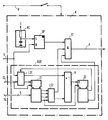
- a memory SP (here a flip-flop) delivers a blocking signal in the form of a logic zero to a first input of a controller ST (here an AND gate with three Entrances). This means that no pulse can appear at output F of channel assignor K - this output is also the output of control ST.
- the capacitor SP of the RC element at the point in time at which the supply voltage U is applied causes the memory SP to be set, that is to say to put it in a state in which it emits the blocking signal mentioned for the control ST.
- the memory SP is reset by the edge of this synchronizing pulse. This creates a logic one at the first input of the control ST. When this logical one is created, a first prerequisite for opening the control ST is fulfilled.
- a synchronous monitoring circuit SÜE is also provided, which carries out the synchronous state monitoring during operation. This monitoring is carried out with the aid of the synchronization signal S, a slot coding SL (here five parallel bits) and a bit clock Cl. All three signals are fed to the channel allocator from the outside.
- the synchronization signal S is applied to a first charge pulse generation circuit LS1, as is the bit clock C1.
- the first charge pulse generation circuit LS1 reacts to the rising edges in the synchronization signal S and is therefore independent of the pulse-pause ratio of this signal.
- a first pulse Z1 is loaded at the beginning of the synchronizing signal S with a number that corresponds to the slot coding SL by a loading pulse, which is derived from a synchronizing pulse of the synchronizing signal S by pulse shortening and occurs at a lower output of the first charging pulse generating circuit LS1.
- the counter Z1 is with the Bit clock Cl is clocked and cycles through its counting range.
- the outputs of the first counter Z1 are connected to a second charge pulse generation circuit LS2.
- a first output of the second charge pulse generation circuit LS2 is connected to a comparator V (here an EXCLUSIVE-OR gate), which compares the timing of the pulses derived from the synchronizing pulses of the synchronizing signal S by shortening (upper output of the circuit LS1) with the pulses on the first Output of the second charge pulse supply circuit LS2 monitored.
- V here an EXCLUSIVE-OR gate
- the non-synchronous state is temporarily stored in that a second counter Z2 connected to the first counter Z1 is cleared by an output pulse from the comparator V.
- counter Z2 is clocked by the most significant stage of counter Z1. If the counter Z2 is at level 1, information about this state is transmitted to the first charge pulse generation circuit LS1, which then prevents the supply of charge pulses to the counter Z1.
- the counter Z1 then runs independently of the synchronizing signal S. During its run, only the comparator V checks whether the synchronized state continues to exist due to the once forced synchronization.
- the control ST is now open for pulses which are present at a second output of the second charge pulse generation circuit LS2 and are supplied to a third input of the control ST.
- the temporal position and the length of these pulses relative to the synchronizing pulses of the synchronizing signal S mark the time windows in which useful data of that channel can be transferred to an internal data bus, e.g. is characterized by the slot coding SL.
Landscapes
- Engineering & Computer Science (AREA)
- Computer Networks & Wireless Communication (AREA)
- Time-Division Multiplex Systems (AREA)
- Data Exchanges In Wide-Area Networks (AREA)
Claims (5)
- Montage de circuit permettant de garantir la délivrance correcte dans le temps de signaux vocaux et d'informations d'identification sur un bus de données interne au système à travers un allocateur de canaux d'un système de transmission d'information numérique, qui contient des unités de canaux périphériques pour le traitement séparé des signaux vocaux et des informations d'identification, caractérisé en ce que :
il comporte un circuit RC (RC) et une mémoire (SP), qui ont pour but, après l'application de la tension d'alimentation, de délivrer un signal d'invalidation sur une période de temporisation déterminée, et
un circuit de surveillance de l'état synchrone (SÜE), qui contient :- un premier circuit générateur d'impulsions de charge (LS1) pour extraire des impulsions de charge d'un signal de synchronisation (S) acheminé de l'extérieur;- un premier compteur (Z1) pour un comptage cyclique, dont la valeur de comptage, après réception d'une impulsion de charge, correspond au codage de l'emplacement d'enfichage (SL) affecté à l'allocateur de canaux;- un comparateur (V) pour produire une impulsion de sortie dans le cas de la non-coïncidence d'une impulsion de charge avec une impulsion produite par le deuxième circuit générateur d'impulsions de charge (LS2) après un parcours du premier compteur (Z1), et- un deuxième compteur (Z2), qui a pour objet, après réception de l'impulsion de sortie, d'interrompre la délivrance d'une impulsion de charge au premier compteur (Z1) et, après comptage d'un nombre prédéterminé de rythmes délivrés par le premier compteur (Z1) et dans le cas de non-délivrance du signal d'invalidation, de valider une impulsion produite par le deuxième circuit générateur d'impulsions de charge en fonction du codage de l'emplacement d'enfichage (SL). - Montage de circuit selon la revendication 1, caractérisé en ce que le premier circuit générateur d'impulsions de charge (LS1) est prévu pour recevoir un rythme binaire (CL) acheminé de l'extérieur et pour produire des impulsions de charge raccourcies vis-à-vis d'une impulsion du signal de synchronisation (S) après l'apparition d'un flanc croissant dans le signal de synchronisation (S).
- Montage de circuit selon la revendication 1 ou 2, caractérisé en ce que le premier compteur (Z1) est prévu pour se synchroniser sur le rythme binaire (C1) acheminé de l'extérieur et pour un parcours cyclique de sa plage de comptage.
- Montage de circuit selon la revendication 1, 2 ou 3, caractérisé en ce que le deuxième compteur (Z2) est prévu pour, après réception de l'impulsion de sortie du comparateur (V), se régler sur une valeur de comptage de départ et compter les impulsions de comptage apparaissant à la sortie la plus significative du premier compteur (Z1) et, une fois atteint un état de comptage prédéterminé, valider la sortie de l'allocateur de canaux.
- Montage de circuit selon la revendication 1, 2, 3 ou 4, caractérisé en ce qu'il est prévu une commande (ST) constituée d'une porte ET, qui reçoit le signal d'invalidation, un signal de sortie du deuxième compteur (Z2) et un signal de sortie du deuxième circuit générateur d'impulsions de charge (LS2) et en ce que la sortie de la commande (ST) constitue la sortie de l'allocateur de canaux (K).
Applications Claiming Priority (2)
| Application Number | Priority Date | Filing Date | Title |
|---|---|---|---|
| DE19873733888 DE3733888A1 (de) | 1987-10-07 | 1987-10-07 | Schaltungsanordnung zur sicherstellung der zeitrichtigen kanalzuordnung in einem digitalen nachrichtenuebertragungssystem |
| DE3733888 | 1987-10-07 |
Publications (3)
| Publication Number | Publication Date |
|---|---|
| EP0311181A2 EP0311181A2 (fr) | 1989-04-12 |
| EP0311181A3 EP0311181A3 (en) | 1990-11-07 |
| EP0311181B1 true EP0311181B1 (fr) | 1994-06-15 |
Family
ID=6337802
Family Applications (1)
| Application Number | Title | Priority Date | Filing Date |
|---|---|---|---|
| EP88202123A Expired - Lifetime EP0311181B1 (fr) | 1987-10-07 | 1988-09-29 | Circuit pour garantir l'allocation exacte en temps de canaux dans un système de commutation de messages numériques |
Country Status (4)
| Country | Link |
|---|---|
| EP (1) | EP0311181B1 (fr) |
| JP (1) | JPH01120923A (fr) |
| CA (1) | CA1327656C (fr) |
| DE (2) | DE3733888A1 (fr) |
Families Citing this family (1)
| Publication number | Priority date | Publication date | Assignee | Title |
|---|---|---|---|---|
| JP4857076B2 (ja) * | 2006-10-31 | 2012-01-18 | 三菱電機システムサービス株式会社 | ウェザーカバー |
Family Cites Families (7)
| Publication number | Priority date | Publication date | Assignee | Title |
|---|---|---|---|---|
| GB2085264A (en) * | 1980-09-12 | 1982-04-21 | Western Electric Co | Digital concentrator |
| US4484323A (en) * | 1982-06-14 | 1984-11-20 | At&T Bell Laboratories | Communication arrangements for distributed control systems |
| DE3311284A1 (de) * | 1983-03-28 | 1984-10-11 | Siemens AG, 1000 Berlin und 8000 München | Schaltungsanordnung zum verhindern der abgabe von stoersignalen |
| DE3311257A1 (de) * | 1983-03-28 | 1984-10-04 | Siemens AG, 1000 Berlin und 8000 München | Schaltungsanordnung zum verhindern der abgabe von stoersignalen |
| DE3311283A1 (de) * | 1983-03-28 | 1984-10-11 | Siemens AG, 1000 Berlin und 8000 München | Schaltungsanordnung zum verhindern der abgabe von stoersignalen |
| JPS6085697A (ja) * | 1983-10-17 | 1985-05-15 | Fujitsu Ltd | タイムスロツト分配方式 |
| US4750136A (en) * | 1986-01-10 | 1988-06-07 | American Telephone And Telegraph, At&T Information Systems Inc. | Communication system having automatic circuit board initialization capability |
-
1987
- 1987-10-07 DE DE19873733888 patent/DE3733888A1/de not_active Withdrawn
-
1988
- 1988-09-29 DE DE3850208T patent/DE3850208D1/de not_active Expired - Fee Related
- 1988-09-29 EP EP88202123A patent/EP0311181B1/fr not_active Expired - Lifetime
- 1988-10-04 CA CA000579227A patent/CA1327656C/fr not_active Expired - Fee Related
- 1988-10-07 JP JP63252170A patent/JPH01120923A/ja active Pending
Also Published As
| Publication number | Publication date |
|---|---|
| EP0311181A2 (fr) | 1989-04-12 |
| JPH01120923A (ja) | 1989-05-12 |
| EP0311181A3 (en) | 1990-11-07 |
| DE3850208D1 (de) | 1994-07-21 |
| DE3733888A1 (de) | 1989-04-27 |
| CA1327656C (fr) | 1994-03-08 |
Similar Documents
| Publication | Publication Date | Title |
|---|---|---|
| DE1223414B (de) | Schaltungsanordnung fuer Codeuebersetzer in Empfangseinrichtungen fuer Nachrichten in fehlerkorrigierendem Code | |
| DE3027579C2 (fr) | ||
| DE69220267T2 (de) | Pulsstopfanlage | |
| DE2942246A1 (de) | Schaltungsanordnung eines elastischen speichers eines pcm-uebertragungssystems | |
| DE3217584A1 (de) | Digitales pcm-uebertragungssystem | |
| EP0023331A1 (fr) | Circuit pour la synchronisation d'un dispositif subordonné, en particulier un poste d'abonné numérique par un dispositif d'ordre supérieur, en particulier un central de communication numérique d'un réseau de télécommunication MIC | |
| DE2437873C2 (de) | Vorrichtung zur Erstellung eines Neutralisierungssignals für einen Echounterdrücker | |
| DE3125724C2 (fr) | ||
| EP0311181B1 (fr) | Circuit pour garantir l'allocation exacte en temps de canaux dans un système de commutation de messages numériques | |
| DE1909726C3 (de) | Zeitmultiplex-Fernsprechvernüttlungsstelle | |
| DE2944777A1 (de) | Schaltungsanordnung eines elastischen speichers, insbesondere eines zeitmultiplexdatenuebertragungssystems | |
| DE2908366C2 (de) | Verfahren und Schaltungsanordnung zur Reduzierung von Phasenschwankungen bei der Taktrückgewinnung in einem digitalen, hierarchisch gegliederten, plesiochronen Nachrichtenübertragungssystem | |
| EP1221220A2 (fr) | Procede et dispositif pour la communication bidirectionnelle entre au moins deux interlocuteurs | |
| DE2620291A1 (de) | Elastischer speicher insbesondere fuer einen asynchron arbeitenden pcm-multiplexer | |
| DE2457611C3 (de) | Multiplex-Übertragungssystem | |
| EP0459005B1 (fr) | Méthode et arrangement de transmission d'information de l'état de fonctionnement entre les dispositifs centraux et décentralisés d'un système de communication | |
| DE2021953C3 (de) | Zeitmultiplexübertragungssystem mit einem Sender und einem Empfänger zur Übertragung von Signalen mittels Pulscodemodulation | |
| DE2432976A1 (de) | Codier- und decodiereinrichtung fuer zeitmultiplex-fernsprechsysteme | |
| DE2261905A1 (de) | Sprachinterpolationsanordnung fuer ein zeitmultiplex-fernmeldesystem | |
| EP0231809B1 (fr) | Procédé pour l'intégration d'un ou de plusieurs modules à fonction supplémentaire dans des centraux téléphoniques ainsi que circuit d'accès pour réaliser le procédé | |
| DE3117927C2 (de) | Anordnung zur Erkennung der längsten von in digitalen Signalen periodisch enthaltenen Folgen von Nullzeichen | |
| DE3153249C2 (en) | Phase discriminator arrangement | |
| EP0271955B1 (fr) | Circuit pour la synchronisation de dispositifs dans des centraux et des stations d'amplification d'un système de transmission par répartition dans le temps | |
| DE2845393C2 (de) | Verfahren zur Überwachung eines Kennzeichen-Umsetzgeräts | |
| DE2734096C2 (de) | Schaltungsanordnung zur Steuerung der Übertragung von Digital-Signalen, insbesondere PCM-Signalen, zwischen Teilnehmerstellen eines Zeitmultiplex-Fernmeldenetzes, insbesondere PCM-Zeitmultiplex- Fernmeldenetzes und einer vierdrahtmäßig betriebenen Zweidraht-Multiplexleitung |
Legal Events
| Date | Code | Title | Description |
|---|---|---|---|
| PUAI | Public reference made under article 153(3) epc to a published international application that has entered the european phase |
Free format text: ORIGINAL CODE: 0009012 |
|
| AK | Designated contracting states |
Kind code of ref document: A2 Designated state(s): DE FR GB IT SE |
|
| PUAL | Search report despatched |
Free format text: ORIGINAL CODE: 0009013 |
|
| AK | Designated contracting states |
Kind code of ref document: A3 Designated state(s): DE FR GB IT SE |
|
| 17P | Request for examination filed |
Effective date: 19910502 |
|
| 17Q | First examination report despatched |
Effective date: 19921117 |
|
| GRAA | (expected) grant |
Free format text: ORIGINAL CODE: 0009210 |
|
| AK | Designated contracting states |
Kind code of ref document: B1 Designated state(s): DE FR GB IT SE |
|
| REF | Corresponds to: |
Ref document number: 3850208 Country of ref document: DE Date of ref document: 19940721 |
|
| ITF | It: translation for a ep patent filed | ||
| GBT | Gb: translation of ep patent filed (gb section 77(6)(a)/1977) |
Effective date: 19940919 |
|
| ET | Fr: translation filed | ||
| EAL | Se: european patent in force in sweden |
Ref document number: 88202123.1 |
|
| PLBE | No opposition filed within time limit |
Free format text: ORIGINAL CODE: 0009261 |
|
| STAA | Information on the status of an ep patent application or granted ep patent |
Free format text: STATUS: NO OPPOSITION FILED WITHIN TIME LIMIT |
|
| ITPR | It: changes in ownership of a european patent |
Owner name: CAMBIO RAGIONE SOCIALE;PHILIPS ELECTRONICS N.V. |
|
| 26N | No opposition filed | ||
| REG | Reference to a national code |
Ref country code: GB Ref legal event code: 732E |
|
| REG | Reference to a national code |
Ref country code: FR Ref legal event code: TP |
|
| REG | Reference to a national code |
Ref country code: GB Ref legal event code: IF02 |
|
| PGFP | Annual fee paid to national office [announced via postgrant information from national office to epo] |
Ref country code: SE Payment date: 20020625 Year of fee payment: 15 |
|
| PGFP | Annual fee paid to national office [announced via postgrant information from national office to epo] |
Ref country code: GB Payment date: 20020827 Year of fee payment: 15 |
|
| PGFP | Annual fee paid to national office [announced via postgrant information from national office to epo] |
Ref country code: DE Payment date: 20020916 Year of fee payment: 15 |
|
| PGFP | Annual fee paid to national office [announced via postgrant information from national office to epo] |
Ref country code: FR Payment date: 20030926 Year of fee payment: 16 |
|
| PG25 | Lapsed in a contracting state [announced via postgrant information from national office to epo] |
Ref country code: GB Free format text: LAPSE BECAUSE OF NON-PAYMENT OF DUE FEES Effective date: 20030929 |
|
| PG25 | Lapsed in a contracting state [announced via postgrant information from national office to epo] |
Ref country code: SE Free format text: LAPSE BECAUSE OF NON-PAYMENT OF DUE FEES Effective date: 20030930 |
|
| PG25 | Lapsed in a contracting state [announced via postgrant information from national office to epo] |
Ref country code: DE Free format text: LAPSE BECAUSE OF NON-PAYMENT OF DUE FEES Effective date: 20040401 |
|
| EUG | Se: european patent has lapsed | ||
| GBPC | Gb: european patent ceased through non-payment of renewal fee |
Effective date: 20030929 |
|
| PG25 | Lapsed in a contracting state [announced via postgrant information from national office to epo] |
Ref country code: FR Free format text: LAPSE BECAUSE OF NON-PAYMENT OF DUE FEES Effective date: 20040528 |
|
| REG | Reference to a national code |
Ref country code: FR Ref legal event code: ST |
|
| PG25 | Lapsed in a contracting state [announced via postgrant information from national office to epo] |
Ref country code: IT Free format text: LAPSE BECAUSE OF NON-PAYMENT OF DUE FEES;WARNING: LAPSES OF ITALIAN PATENTS WITH EFFECTIVE DATE BEFORE 2007 MAY HAVE OCCURRED AT ANY TIME BEFORE 2007. THE CORRECT EFFECTIVE DATE MAY BE DIFFERENT FROM THE ONE RECORDED. Effective date: 20050929 |