EP0312016A2 - Linearer Differenzverstärker - Google Patents
Linearer Differenzverstärker Download PDFInfo
- Publication number
- EP0312016A2 EP0312016A2 EP88116943A EP88116943A EP0312016A2 EP 0312016 A2 EP0312016 A2 EP 0312016A2 EP 88116943 A EP88116943 A EP 88116943A EP 88116943 A EP88116943 A EP 88116943A EP 0312016 A2 EP0312016 A2 EP 0312016A2
- Authority
- EP
- European Patent Office
- Prior art keywords
- emitter
- transistors
- transistor
- currents
- differential amplifier
- Prior art date
- Legal status (The legal status is an assumption and is not a legal conclusion. Google has not performed a legal analysis and makes no representation as to the accuracy of the status listed.)
- Withdrawn
Links
Images


Classifications
-
- H—ELECTRICITY
- H03—ELECTRONIC CIRCUITRY
- H03F—AMPLIFIERS
- H03F1/00—Details of amplifiers with only discharge tubes, only semiconductor devices or only unspecified devices as amplifying elements
- H03F1/32—Modifications of amplifiers to reduce non-linear distortion
- H03F1/3211—Modifications of amplifiers to reduce non-linear distortion in differential amplifiers
Definitions
- the present invention relates to a linear differential amplifier which constitutes a part of an electric filter or a similar device to be incorporated, for example, in an IC.
- V cc stands for the power source voltage.
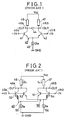
- an emitter-coupled pair formed by bipolar transistors like the one shown in Fig. 1 possesses a poor linearity and changes its transconductance depending on the level of input signals. Consequently, an electric filter comprised of a differential amplifier of this type changes its characteristic depending on the level of input signals, and therefore is not satisfactory in this respect.
- This differential amplifier is comprised of two emitter-coupled pairs 40 and 50 formed by a pair of transistors 51 and 52, and 53 and 54, respectively, where each of the transistors 52 and 54 has an emitter area four times larger than that of the transistors 51 and 53.
- Collectors of the transistors 52 and 53 are connected with each other as well as with a load resistor 46 which converts output currents I3 of these two transistors, while collectors of transistors 51 and 54 are connected with each other as well as with a load resistor 47 which converts output currents I4 of these two transistors. It further includes a constant current source 55 for the emitter-coupled pair 40 for supplying emitter currents I e , and a constant current source 56 for the emitter-coupled pair 50 for supplying emitter currents I e , output terminals 48A and 48B connected to the collectors of the transistors 52 and 53, and 51 and 54, respectively, input terminals 49A and 49B connected to the bases of the transistors 52 and 53, and 51 and 54, respectively.
- Vcc stands for the power source voltage in Fig.2.
- the improvement of the linearity is achieved by producing output currents I3 and I4 as sums of the collector currents with an offset ratio of 1:4 from the transistors of the emitter-coupled pairs 40 and 50, the offset being caused by the fact that these emitter-coupled pairs 40 and 50 are comprised of transistors with an emitter area ratio of 1:4.
- Fig. 3 shows the input-output characteristic of this differential amplifier contrasted against that of the conventional one.
- a curve A is the characteristic curve of the differential amplifier of Fig. 2 while a curve B is the characteristic curve of the differential amplifier of Fig. 1, and R L is the resistance of the load.
- a gyrator or a biquad filter By constructing a gyrator or a biquad filter with such a differential amplifier of an improved linearity, an improvement can be made in a frequency characteristic by regarding the differential amplifier as a single stage integrator, but to obtain a high direct current gain becomes difficult.
- the lowering of a direct current gain in an integrator of an electric filter causes the lowering of a quality Q of the device that includes the electric filter, as can be seen from a comparison to a passive filter comprised of an LC circuit.
- connecting a differential amplifier of Fig. 2 to an emitter-follower is equivalent to connecting a transistor with an emitter area five times larger than the minimal emitter area available. Since a base-emitter capacitance of a transistor is proportional to an emitter area, when an emitter area is five times larger as in this case, a base emitter capacitance also becomes five times greater.
- the aforementioned differential amplifier with its output terminals connected to emitter-followers can be considered as a low-pass filter shown in Fig. 4(A) or its equivalent circuit shown in Fig. 4(B) formed by a base-emitter capacitance C be and output resistance r o and a base resistance r b of the emitter-follower 57.
- V cc is the power source voltage
- V in is an input voltage
- V out is an output voltage.
- a linear differential amplifier comprising: a pair of first and second transistors with their emitters coupled to each other; a pair of third and fourth transistors with their emitters coupled to each other, a collector of the first transistor being connected to a collector of the third transistor and a collector of the second transistor being connected to a collector of the fourth transistor; a pair of input terminals, one of which being coupled to the base of the first transistor, the other one of which being coupled to the base of the fourth transistor; a pair of output terminals, one of which being connected to the collectors of the first and the third transistors, the other one of which being connected to the collectors of the second and the fourth transistors; constant current source means for supplying emitter currents to the transistors; and load resistor means for converting collector currents of the transistors into output voltages, characterized by comprising: first voltage source means for applying first offset DC voltages between one of the input terminals and a base of the third transistor; second voltage source means for applying second offset DC voltages
- a linear differential amplifier is comprised of a first emitter-coupled pair 10 formed by two transistors Q1 and Q2, a second emitter-coupled pair 20 formed by two transistors Q3 and Q4, where a collector 11 of the transistor Q1 is connected to a collector 13 of the transistor Q3 and a collector 12 of the transistor Q2 is connected to a collector 14 of the transistor Q4, a first constant voltage source E1 for applying a constant voltage between a base 1 of the transistor Q1 and a base 3 of the transistor Q3, a second constant voltage source E2 for applying the same voltage applied by the first constant voltage source E1 but in the opposite direction between a base 2 of the transistor Q2 and a base 4 of the transistor Q4, a first load resistor 5 for converting collector currents of the transistors Q1 and Q3 shown collectively as an output current I1 into an output voltage, a second load resistor 6 for converting collector currents of the transistor
- a base 1 of the transistor Q1 and a base 3 of the transistor Q3 are connected to an input terminal 17, a base 2 of the transistor Q2 and a base 4 of the transistor Q4 are connected to an input terminal 18, and the amplifier is emitter-grounded as shown.
- V cc stands for the power source voltage.
- the improved linearity is achieved in this linear differential amplifier, as in the prior art explained above, by obtaining output currents I1 and I2 as sums of collector currents with offsets.
- offsets are produced, not by the difference of the emitter areas of transistors as in the prior art, but by the constant offset voltage applied by the constant voltage sources E1 and E2. Therefore, transistors Q1, Q2, Q3 and Q4 of the emitter-coupled pairs 10 and 20 do not need to have a large emitter area ratio. In fact, they can be of minimum size available. Consequently, the improved linearity can be achieved in this embodiment while maintaining a high S/N ratio, a good high-frequency characteristic, a high direct current gain, and a high-speed operation capability, by incorporating appropriate configurations.
- the constant voltage sources, E1 and E2 in the last embodiment are comprised of pairs of emitter-followers 21 and 22, and 23 and 24.
- Each pair is comprised of emitter-followers including transistors with an emitter area ratio of 1:4, and each emitter-follower is connected to an emitter current source for a transistor.
- the constant voltage source for the transistors Q1 and Q3 is comprised of the emitter-followers 21 and 22 where the emitter-follower 22 has a transistor Q6 with an emitter area four times larger than that of a transistor Q5 of the emitter-follower 21, and the the emitter-followers 21 and 22 are connected to emitter current sources 25a and 25b, respectively, which supply emitter currents I o to the transistors Q5 and Q6, respectively.
- the constant voltage source for the transistors Q2 and Q4 is comprised of the emitter-followers 23 and 24 where the emitter-follower 24 has a transistor Q8 with an emitter area four times larger than that of a transistor Q7 of the emitter follower 23, and the emitter followers 23 and 24 are connected to emitter current sources 25c and 25d, respectively, which supply emitter currents I o to the transistors Q7 and Q8, respectively.
- V be (Q6) Vt ln (I c /4I s (V)
- I s is the saturation current of the transistors
- I c is the collector current of the transistors
- V t is the thermal voltage of the transistors.
- the improved linearity is achieved in this embodiment, just as in the last embodiment, by obtaining output currents I1 and I2 as sum of the collector currents with offsets.
- the emitter-followers it is possible in this embodiment to achieve the improved linearity while maintaining a high S/N ratio, a good high-frequency characteristic, a high direct current gain, and a high-speed operation capability. This is because, as in the last embodiment, the transistors Q1, Q2, Q3 and Q4 do not need to have a larger emitter area ratio, and can be of minimum size.
- Fig. 7 there is shown another embodiment of a linear differential amplifier according to the present invention.
- constant voltage sources in the embodiment of Fig. 6 is modified such that the transistors of the paired emitter-followers Q5 and Q9, Q7 and Q10 now have the same emitter areas, but at the same time the transistors Q5 and Q7 are connected to the emitter current sources 30a and 30b, respectively, which supply emitter currents 4I o which is four times greater than that supplied by the emitter current sources 25b and 25d to the transistors Q9 and Q10.
- Fig. 8 there is shown another embodiment of a linear differential amplifier according to the present invention.
- constant voltage sources in the embodiment of Fig. 6 is modified such that each pair transistors of the paired emitter-followers Q5 and Q13, and Q7 and Q14 now have an emitter area ratio of 1:2, but at the same time transistors of the emitter-coupled pairs, Q1 and Q4 in the embodiment of Fig. 6, are also replaced by transistors Q11 and Q12 which have the emitter area twice larger than that of the transistors Q2 and Q3.
- each of the constant current sources, 7 and 8 in the embodiment of Fig. 6, and the emitter current sources, 25a, 25b, 25c and 25d in the embodiment of Fig. 2 are comprised of a transistor with a resistor connected between its emitter and the ground.
- the constant current source for the transistors Q1 and Q2 is comprised of a transistor Q15 with a resistor 33a connected between its emitter and the ground
- the constant current source for the transistors Q3 and Q4 is comprised of a transistor Q16 with a resistor 33b connected between its emitter and the ground, where these transistors Q15 and Q16 are biased by the constant voltage 34.
- the emitter current source for the transistor Q5 is comprised of a transistor Q17 with a resistor 35a connected between its emitter and the ground
- the emitter current source for the transistor Q6 is comprised of a transistor Q18 with a resistor 35b connected between its emitter and the ground
- the emitter current source for the transistor Q7 is comprised of a transistor Q19 with a resistor 35c connected between its emitter and the ground
- the emitter current source for the transistor Q8 is comprised of a transistor Q20 with a resistor 35d connected between its emitter and the ground, where these transistors Q17, Q18 Q19 and Q20 are biased by the constant voltage 36.
- Fig. 10 there is shown another embodiment a linear differential amplifier according to the present invention.
- the linear differential amplifier of Fig. 5 is modified by connecting diodes D1, D2, D3 or D4 between the emitter of each of the transistors Q1, Q2, Q3 or Q4 and the constant current sourcc 7 or 8.
- a linear differential amplifier of the present invention can be utilized not only in an electric filter, but anywhere where the improved linearity of an amplifier is desirable such as, for example, an initial stage for an amplifier of operational amplifier type.
Landscapes
- Physics & Mathematics (AREA)
- Nonlinear Science (AREA)
- Engineering & Computer Science (AREA)
- Power Engineering (AREA)
- Amplifiers (AREA)
Applications Claiming Priority (2)
| Application Number | Priority Date | Filing Date | Title |
|---|---|---|---|
| JP254783/87 | 1987-10-12 | ||
| JP62254783A JP2603968B2 (ja) | 1987-10-12 | 1987-10-12 | 線形差動増幅回路 |
Publications (2)
| Publication Number | Publication Date |
|---|---|
| EP0312016A2 true EP0312016A2 (de) | 1989-04-19 |
| EP0312016A3 EP0312016A3 (de) | 1990-03-07 |
Family
ID=17269819
Family Applications (1)
| Application Number | Title | Priority Date | Filing Date |
|---|---|---|---|
| EP88116943A Withdrawn EP0312016A3 (de) | 1987-10-12 | 1988-10-12 | Linearer Differenzverstärker |
Country Status (3)
| Country | Link |
|---|---|
| US (2) | US5006818A (de) |
| EP (1) | EP0312016A3 (de) |
| JP (1) | JP2603968B2 (de) |
Cited By (7)
| Publication number | Priority date | Publication date | Assignee | Title |
|---|---|---|---|---|
| EP0397265A1 (de) * | 1989-05-12 | 1990-11-14 | Koninklijke Philips Electronics N.V. | Bipolare Transistorschaltung mit Verzerrungsausgleich |
| EP0352009A3 (en) * | 1988-07-18 | 1990-11-14 | Sony Corp | Amplifier circuit |
| EP0352790A3 (de) * | 1988-07-28 | 1991-07-10 | Kabushiki Kaisha Toshiba | Integrator und aktives Filter mit Phasenkompensierung |
| US5079515A (en) * | 1989-05-31 | 1992-01-07 | Kabushiki Kaisha Toshiba | Linearized differential amplifier |
| DE4104981C1 (en) * | 1991-02-19 | 1992-09-17 | Telefunken Electronic Gmbh, 7100 Heilbronn, De | Differential amplifier circuit for HF mixer - uses two complementary transistor pairs with common connection of emitters, and collectors connected via capacitors |
| EP0601560A1 (de) * | 1992-12-08 | 1994-06-15 | Nec Corporation | Differenzverstärkerschaltung |
| EP1056194A1 (de) * | 1999-05-26 | 2000-11-29 | Philips Patentverwaltung GmbH | Transistorverstärker |
Families Citing this family (40)
| Publication number | Priority date | Publication date | Assignee | Title |
|---|---|---|---|---|
| US5122759A (en) * | 1990-10-25 | 1992-06-16 | Texas Instruments Incorporated | Class-A differential amplifier and method |
| EP0501827B1 (de) * | 1991-03-01 | 1996-04-17 | Kabushiki Kaisha Toshiba | Multiplizierschaltung |
| GB2256550B (en) * | 1991-06-04 | 1995-08-02 | Silicon Systems Inc | Differential pair based transconductance element with improved linearity and signal to noise ratio |
| GB2268015A (en) * | 1992-06-18 | 1993-12-22 | Gould Inc | Feed-forward distortion reduction for transconductance amplifier |
| JP3315748B2 (ja) * | 1993-02-19 | 2002-08-19 | 三菱電機株式会社 | 増幅回路 |
| US5523717A (en) * | 1993-11-10 | 1996-06-04 | Nec Corporation | Operational transconductance amplifier and Bi-MOS multiplier |
| US5420538A (en) * | 1994-06-10 | 1995-05-30 | Northern Telecom Limited | Linear bipolar junction transistor amplifier |
| JPH11504791A (ja) * | 1996-03-05 | 1999-04-27 | フィリップス エレクトロニクス ネムローゼ フェンノートシャップ | 演算増幅器 |
| US5990740A (en) * | 1997-12-02 | 1999-11-23 | Nokia Mobile Phones | Differential amplifier with adjustable linearity |
| US6084472A (en) * | 1997-12-15 | 2000-07-04 | Analog Devices, Inc. | Multi-tanh triplet with optimal biasing |
| US6081572A (en) * | 1998-08-27 | 2000-06-27 | Maxim Integrated Products | Lock-in aid frequency detector |
| JP2002524899A (ja) | 1998-08-31 | 2002-08-06 | マキシム・インテグレイテッド・プロダクツ・インコーポレイテッド | 線形及び複合sinhトランスコンダクタンス回路 |
| US6188281B1 (en) | 1998-09-30 | 2001-02-13 | Maxim Integrated Products, Inc. | Linear transconductance circuits having class AB amplifiers parallel coupled with concave compensation circuits |
| US6271725B1 (en) * | 1998-09-30 | 2001-08-07 | Lsi Logic Corporation | Low voltage bipolar transconductor circuit with extended dynamic range |
| JP3644387B2 (ja) * | 2001-01-10 | 2005-04-27 | ソニー株式会社 | フィルタ回路 |
| CN1198389C (zh) * | 2001-05-11 | 2005-04-20 | 三洋电机株式会社 | 正弦值产生电路、相移电路、色调调整电路 |
| US7171170B2 (en) | 2001-07-23 | 2007-01-30 | Sequoia Communications | Envelope limiting for polar modulators |
| US6798290B2 (en) * | 2001-08-31 | 2004-09-28 | Sequoia Communications | Translinear variable gain amplifier |
| US6985703B2 (en) | 2001-10-04 | 2006-01-10 | Sequoia Corporation | Direct synthesis transmitter |
| US7489916B1 (en) | 2002-06-04 | 2009-02-10 | Sequoia Communications | Direct down-conversion mixer architecture |
| US7496338B1 (en) | 2003-12-29 | 2009-02-24 | Sequoia Communications | Multi-segment gain control system |
| US7609118B1 (en) | 2003-12-29 | 2009-10-27 | Sequoia Communications | Phase-locked loop calibration system |
| US7522017B1 (en) | 2004-04-21 | 2009-04-21 | Sequoia Communications | High-Q integrated RF filters |
| US7672648B1 (en) | 2004-06-26 | 2010-03-02 | Quintics Holdings | System for linear amplitude modulation |
| US7479815B1 (en) | 2005-03-01 | 2009-01-20 | Sequoia Communications | PLL with dual edge sensitivity |
| US7548122B1 (en) | 2005-03-01 | 2009-06-16 | Sequoia Communications | PLL with switched parameters |
| US7675379B1 (en) | 2005-03-05 | 2010-03-09 | Quintics Holdings | Linear wideband phase modulation system |
| US7595626B1 (en) | 2005-05-05 | 2009-09-29 | Sequoia Communications | System for matched and isolated references |
| JP4723394B2 (ja) * | 2006-02-13 | 2011-07-13 | 新日本無線株式会社 | 演算増幅器 |
| US20070205200A1 (en) * | 2006-03-02 | 2007-09-06 | Brain Box Concepts | Soap bar holder and method of supporting a soap bar |
| WO2007137094A2 (en) | 2006-05-16 | 2007-11-29 | Sequoia Communications | A multi-mode vco for direct fm systems |
| US7522005B1 (en) | 2006-07-28 | 2009-04-21 | Sequoia Communications | KFM frequency tracking system using an analog correlator |
| US7679468B1 (en) | 2006-07-28 | 2010-03-16 | Quintic Holdings | KFM frequency tracking system using a digital correlator |
| US7894545B1 (en) | 2006-08-14 | 2011-02-22 | Quintic Holdings | Time alignment of polar transmitter |
| US7920033B1 (en) | 2006-09-28 | 2011-04-05 | Groe John B | Systems and methods for frequency modulation adjustment |
| US7463094B2 (en) * | 2007-03-30 | 2008-12-09 | Don Roy Sauer | Linearized class AB biased differential input stage |
| CN103140737B (zh) * | 2010-09-30 | 2015-09-16 | 西铁城控股株式会社 | 物理量传感器 |
| JP5956983B2 (ja) * | 2011-04-25 | 2016-07-27 | シチズンホールディングス株式会社 | アナログ乗算回路、可変ゲインアンプ、検波回路及び物理量センサ |
| US9944245B2 (en) | 2015-03-28 | 2018-04-17 | Amsafe, Inc. | Extending pass-through airbag occupant restraint systems, and associated systems and methods |
| US11239807B1 (en) | 2020-12-01 | 2022-02-01 | Microsoft Technology Licensing, Llc | Offset compensated differential amplifier and calibration circuit providing increased linear range and granularity of offset compensation and related method |
Family Cites Families (4)
| Publication number | Priority date | Publication date | Assignee | Title |
|---|---|---|---|---|
| US4146844A (en) * | 1977-10-31 | 1979-03-27 | Tektronix, Inc. | Feed-forward amplifier |
| JPS5634207A (en) * | 1979-08-30 | 1981-04-06 | Toshiba Corp | Differential amplifier |
| DE3027071A1 (de) * | 1980-07-17 | 1982-02-11 | Philips Patentverwaltung Gmbh, 2000 Hamburg | Transistorverstaerker mit zwei emittergekoppelten transisorpaaren |
| JPS5857807A (ja) * | 1981-10-02 | 1983-04-06 | Sony Corp | 電圧制御可変利得回路 |
-
1987
- 1987-10-12 JP JP62254783A patent/JP2603968B2/ja not_active Expired - Lifetime
-
1988
- 1988-10-12 EP EP88116943A patent/EP0312016A3/de not_active Withdrawn
-
1990
- 1990-03-27 US US07/500,044 patent/US5006818A/en not_active Expired - Lifetime
-
1999
- 1999-03-08 US US09/264,034 patent/USRE36861E/en not_active Expired - Lifetime
Cited By (10)
| Publication number | Priority date | Publication date | Assignee | Title |
|---|---|---|---|---|
| EP0352009A3 (en) * | 1988-07-18 | 1990-11-14 | Sony Corp | Amplifier circuit |
| EP0352790A3 (de) * | 1988-07-28 | 1991-07-10 | Kabushiki Kaisha Toshiba | Integrator und aktives Filter mit Phasenkompensierung |
| US5081423A (en) * | 1988-07-28 | 1992-01-14 | Kabushiki Kaisha Toshiba | Integrator and active filter including integrator with simple phase compensation |
| EP0397265A1 (de) * | 1989-05-12 | 1990-11-14 | Koninklijke Philips Electronics N.V. | Bipolare Transistorschaltung mit Verzerrungsausgleich |
| US5079515A (en) * | 1989-05-31 | 1992-01-07 | Kabushiki Kaisha Toshiba | Linearized differential amplifier |
| DE4104981C1 (en) * | 1991-02-19 | 1992-09-17 | Telefunken Electronic Gmbh, 7100 Heilbronn, De | Differential amplifier circuit for HF mixer - uses two complementary transistor pairs with common connection of emitters, and collectors connected via capacitors |
| EP0601560A1 (de) * | 1992-12-08 | 1994-06-15 | Nec Corporation | Differenzverstärkerschaltung |
| US5500623A (en) * | 1992-12-08 | 1996-03-19 | Nec Corporation | Differential amplifier circuit with almost linear transconductance |
| EP0809351A3 (de) * | 1992-12-08 | 1998-03-04 | Nec Corporation | Differenzverstärkerschaltung |
| EP1056194A1 (de) * | 1999-05-26 | 2000-11-29 | Philips Patentverwaltung GmbH | Transistorverstärker |
Also Published As
| Publication number | Publication date |
|---|---|
| JP2603968B2 (ja) | 1997-04-23 |
| US5006818A (en) | 1991-04-09 |
| JPH0198306A (ja) | 1989-04-17 |
| EP0312016A3 (de) | 1990-03-07 |
| USRE36861E (en) | 2000-09-12 |
Similar Documents
| Publication | Publication Date | Title |
|---|---|---|
| EP0312016A2 (de) | Linearer Differenzverstärker | |
| US4904952A (en) | Differential amplifier incorporating negative resistance | |
| US5384501A (en) | Integration circuit including a differential amplifier having a variable transconductance | |
| EP0058448B1 (de) | Steilheitsverstärker | |
| US5610547A (en) | Logarithmic transformation circuitry for use in semiconductor integrated circuit devices | |
| US5227681A (en) | Integration circuit | |
| US5280199A (en) | Differential input circuit and operational amplifier with wide common mode input voltage range | |
| US5465072A (en) | Tunable operational transcondunctance amplifier having high linearity | |
| US5557238A (en) | Differential amplifier with common mode regulation | |
| EP0370725B1 (de) | Verstärkerschaltung mit Rückkopplungslast | |
| US5345190A (en) | Modular low voltage filter with common mode feedback | |
| EP0352790B1 (de) | Integrator und aktives Filter mit Phasenkompensierung | |
| EP0500694A1 (de) | Voll differentieller cmos-leistungsverstärker. | |
| GB2107947A (en) | Improvements in or relating to transistor mixer and amplifier input stages for radio receivers | |
| CA1055576A (en) | Operational amplifier | |
| US4686487A (en) | Current mirror amplifier | |
| US4404529A (en) | Lowpass filter with electronic control of cutoff and resonance | |
| US5189321A (en) | Companding current-mode transconductor-c integrator | |
| US6278299B1 (en) | Voltage to current converter | |
| JP3242422B2 (ja) | 広帯域増幅器 | |
| US4689580A (en) | Active filter circuit | |
| US5177382A (en) | Active filter circuit | |
| JPH07240663A (ja) | アクティブフィルタ回路 | |
| KR102857092B1 (ko) | 광대역 고선형성의 가변 이득 증폭기 및 그 방법 | |
| JP3250884B2 (ja) | 演算増幅器 |
Legal Events
| Date | Code | Title | Description |
|---|---|---|---|
| PUAI | Public reference made under article 153(3) epc to a published international application that has entered the european phase |
Free format text: ORIGINAL CODE: 0009012 |
|
| 17P | Request for examination filed |
Effective date: 19881012 |
|
| AK | Designated contracting states |
Kind code of ref document: A2 Designated state(s): DE FR GB |
|
| PUAL | Search report despatched |
Free format text: ORIGINAL CODE: 0009013 |
|
| AK | Designated contracting states |
Kind code of ref document: A3 Designated state(s): DE FR GB |
|
| 17Q | First examination report despatched |
Effective date: 19920429 |
|
| STAA | Information on the status of an ep patent application or granted ep patent |
Free format text: STATUS: THE APPLICATION IS DEEMED TO BE WITHDRAWN |
|
| 18D | Application deemed to be withdrawn |
Effective date: 19920910 |