EP0312986A1 - Procédé de décapage du tungstène avec une sous-couche de nitrure de titane dans des trous de contact de circuits intégrés - Google Patents
Procédé de décapage du tungstène avec une sous-couche de nitrure de titane dans des trous de contact de circuits intégrés Download PDFInfo
- Publication number
- EP0312986A1 EP0312986A1 EP88117336A EP88117336A EP0312986A1 EP 0312986 A1 EP0312986 A1 EP 0312986A1 EP 88117336 A EP88117336 A EP 88117336A EP 88117336 A EP88117336 A EP 88117336A EP 0312986 A1 EP0312986 A1 EP 0312986A1
- Authority
- EP
- European Patent Office
- Prior art keywords
- etching
- tungsten
- titanium nitride
- contact holes
- layer
- Prior art date
- Legal status (The legal status is an assumption and is not a legal conclusion. Google has not performed a legal analysis and makes no representation as to the accuracy of the status listed.)
- Withdrawn
Links
Images
Classifications
-
- H—ELECTRICITY
- H10—SEMICONDUCTOR DEVICES; ELECTRIC SOLID-STATE DEVICES NOT OTHERWISE PROVIDED FOR
- H10P—GENERIC PROCESSES OR APPARATUS FOR THE MANUFACTURE OR TREATMENT OF DEVICES COVERED BY CLASS H10
- H10P50/00—Etching of wafers, substrates or parts of devices
- H10P50/20—Dry etching; Plasma etching; Reactive-ion etching
- H10P50/26—Dry etching; Plasma etching; Reactive-ion etching of conductive or resistive materials
- H10P50/264—Dry etching; Plasma etching; Reactive-ion etching of conductive or resistive materials by chemical means
- H10P50/266—Dry etching; Plasma etching; Reactive-ion etching of conductive or resistive materials by chemical means by vapour etching only
- H10P50/267—Dry etching; Plasma etching; Reactive-ion etching of conductive or resistive materials by chemical means by vapour etching only using plasmas
-
- H—ELECTRICITY
- H10—SEMICONDUCTOR DEVICES; ELECTRIC SOLID-STATE DEVICES NOT OTHERWISE PROVIDED FOR
- H10W—GENERIC PACKAGES, INTERCONNECTIONS, CONNECTORS OR OTHER CONSTRUCTIONAL DETAILS OF DEVICES COVERED BY CLASS H10
- H10W20/00—Interconnections in chips, wafers or substrates
- H10W20/01—Manufacture or treatment
- H10W20/031—Manufacture or treatment of conductive parts of the interconnections
- H10W20/062—Manufacture or treatment of conductive parts of the interconnections by smoothing of conductive parts, e.g. by planarisation
Definitions
- the invention relates to a method for etching back the contact holes for the filling of differently deep contact holes in highly integrated silicon semiconductor circuits on the tungsten layer applied over the entire surface of the substrate containing the contact holes, which contains an underlay consisting of titanium / titanium nitride as an intermediate layer to the substrate.
- CVD c hemical v apor d eposition
- the contact layer it must have a low electrical contact resistance to n+-, p+-doped silicon and silicides, have stable interfaces during temperature storage and have good adhesion to silicon and doped silicon oxide.
- the CVD tungsten must adhere well to this contact layer at the process temperatures used and must be compatible with this material.
- the CVD tungsten layer is non-selectively deposited and covers thus the entire surface of the front side of the Si wafers until the etching back process. In order to avoid particles and to ensure good contact with underlying structures, the CVD tungsten layer must show very good adhesion to the contact layer.
- German patent application P 36 40 656.3 proposes using a titanium / titanium nitride structure as the contact layer.
- CVD tungsten is deposited on this titanium / titanium nitride layer, which acts as a diffusion barrier layer, until the contact hole is securely filled and then the tungsten is etched back together with the titanium / titanium nitride double layer until only the contact hole is filled with tungsten (see FIG. 1 there).
- the advantage of this layer structure is that the titanium layer produces very low contact resistances; the titanium nitride layer prevents direct contact between tungsten and process gases (tungsten hexafluoride) used in the deposition with the silicon substrate; it is also a very good adhesive layer for tungsten.
- etch-back processes such as planar structures can no longer be used.
- the object of the invention is therefore to provide an etch-back method with which CVD tungsten as a contact hole filler can be etched selectively to titanium / titanium nitride, so that even with the same etchant, the titanium nitride serves as an etch stop.
- This object is achieved in a method of the type mentioned above in that a plasma etching process is carried out in a single-disc magnetron etching system in an etching gas containing fluorine ions and oxygen and the end point of the etching is an etching stop on titanium nitride by emission spectroscopy using a wavelength at the maximum of Emission continuum is determined.
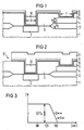
- FIGS. 1 to 3 Show Figures 1 and 2 in a sectional view of the process steps essential to the invention and 3 shows a diagram of the curve of the signal for the end point detection as an etch stop on titanium nitride.
- Figure 1 On the silicon substrate identified by the reference numeral 1, in which there is an n+- or p+-doped zone 2 to be contacted and on which a polysilicon structure 4 is arranged on the field oxide region 3, one serving as an insulation layer or intermediate oxide is provided Phosphorus- and boron-doped SiO2 layer 5 applied, in the contact holes 6 and 7 with a diameter smaller than 1 ⁇ m in the area of the doped zone 2 and the polysilicon layer structure 4 with different contact hole depths are etched.
- the topology of the base with the contact holes 6 and 7 of different depths can be seen from FIG. Due to the field oxide regions 3 and the polysilicon layer structure 4, there are already two height differences h 1 and h 2.
- a 20 nm thick titanium layer 8 and then a 100 nm thick titanium nitride layer 9 are placed on the arrangement (1 to 7) dusted. Then a tungsten layer 10 is applied without a direct pretreatment in a layer thickness of 700 nm by thermal decomposition of tungsten hexafluoride and hydrogen.
- a plasma etching process is used which is carried out on a magnetron single-disk etching system, as is proposed, for example, in German patent application P 37 04 055.3. is carried out.
- the gases used here are sulfur hexafluoride (SF6, purity 99.99%) and oxygen (O2, purity 99.99%).
- the other parameters are: Pressure in the system 0.5 - 1.0 Pa Total flow of gases 70 sccm Oxygen content 20 vol% RF power 400 W. Etching speed 250 nm / min (no loading effect).
- the selectivity of tungsten to titanium nitride is greater than 30: 1 in the process according to the invention and the total etching removal is less than 10 nm with an overetching time of 15 percent.
- the uniformity found is better than ⁇ 7%.
- FIG. 2 After the etching back process according to the teaching of the invention, the conductor track 11 consisting of an aluminum / silicon alloy is now applied, which is structured together with the titanium / titanium nitride layer 8, 9 underneath (see arrow 12).
- Figure 3 The end point detection for the etching back process takes place via emission spectroscopy, the detected wavelength is 576 nm (maximum of the emission continuum).
- the etching time in seconds is plotted as the abscissa, and the intensity J is plotted in arbitrary units as the ordinate.
- the course of the signal for the end point detection as an etch stop on titanium trid applies to a 700 nm thick tungsten layer.
- the end point of the etching (if there is no residue) lies in an end point interval (see small double arrow I) of approximately 15 seconds to 30 seconds after "zero contact" of the plasma intensity.
- the position of the end point interval depends on the topography and layer thickness and must be determined beforehand with control measurements (optical microscope, scanning electron microscope).
- the arrow II drawn to the right at the slope of the curve, indicates the overetching time.
Landscapes
- Internal Circuitry In Semiconductor Integrated Circuit Devices (AREA)
- Drying Of Semiconductors (AREA)
Applications Claiming Priority (2)
| Application Number | Priority Date | Filing Date | Title |
|---|---|---|---|
| DE3735813 | 1987-10-22 | ||
| DE3735813 | 1987-10-22 |
Publications (1)
| Publication Number | Publication Date |
|---|---|
| EP0312986A1 true EP0312986A1 (fr) | 1989-04-26 |
Family
ID=6338880
Family Applications (1)
| Application Number | Title | Priority Date | Filing Date |
|---|---|---|---|
| EP88117336A Withdrawn EP0312986A1 (fr) | 1987-10-22 | 1988-10-18 | Procédé de décapage du tungstène avec une sous-couche de nitrure de titane dans des trous de contact de circuits intégrés |
Country Status (2)
| Country | Link |
|---|---|
| EP (1) | EP0312986A1 (fr) |
| JP (1) | JPH01130529A (fr) |
Cited By (7)
| Publication number | Priority date | Publication date | Assignee | Title |
|---|---|---|---|---|
| WO1991010261A1 (fr) * | 1990-01-04 | 1991-07-11 | International Business Machines Corporation | Structure d'interconnexion pour dispositif semiconducteur utilisant un isolateur en polyimide |
| EP0469214A1 (fr) * | 1990-07-31 | 1992-02-05 | International Business Machines Corporation | Procédé pour la fabrication de domaines en polysilicium conducteur et/ou résistant en couches superposées dans des dispositifs à semiconducteurs multiniveaux et structures résultantes |
| DE4132564A1 (de) * | 1991-09-30 | 1993-04-08 | Siemens Ag | Verfahren zum plasmaaetzen mit mikrowellenenergiegespeister voranregung der aetzgase bei der herstellung integrierter halbleiterschaltungen |
| EP0703606A3 (fr) * | 1994-09-20 | 1998-03-11 | Siemens Aktiengesellschaft | Procédé pour éviter le re-dépÔt de produits de gravure sur la surface de substrats pendant la rétro-gravure de tungstène au cours de la fabrication de circuits à haute densité d'intégration |
| US5889328A (en) * | 1992-02-26 | 1999-03-30 | International Business Machines Corporation | Refractory metal capped low resistivity metal conductor lines and vias |
| WO2001069654A3 (fr) * | 2000-03-13 | 2002-01-10 | Koninkl Philips Electronics Nv | Dispositif semi-conducteur et procede de gravure |
| US7031350B2 (en) | 2000-07-17 | 2006-04-18 | Koninklijke Philips Electronics N.V. | Coding of data stream |
Families Citing this family (4)
| Publication number | Priority date | Publication date | Assignee | Title |
|---|---|---|---|---|
| JPH04152550A (ja) * | 1990-10-16 | 1992-05-26 | Oki Electric Ind Co Ltd | 半導体装置の製造方法 |
| JPH0555220A (ja) * | 1991-08-26 | 1993-03-05 | Nec Corp | 半導体装置の製造方法 |
| JP2882339B2 (ja) * | 1996-02-21 | 1999-04-12 | 日本電気株式会社 | タングステンcvd反応室内のエッチング方法 |
| US7183215B2 (en) * | 2004-07-21 | 2007-02-27 | Hewlett-Packard Development Company, L.P. | Etching with electrostatically attracted ions |
Citations (2)
| Publication number | Priority date | Publication date | Assignee | Title |
|---|---|---|---|---|
| US4566026A (en) * | 1984-04-25 | 1986-01-21 | Honeywell Inc. | Integrated circuit bimetal layer |
| EP0169082A1 (fr) * | 1984-05-11 | 1986-01-22 | Societe Pour L'etude Et La Fabrication De Circuits Integres Speciaux - E.F.C.I.S. | Procédé de fabrication de circuits intégrés à plusieurs niveaux d'interconnexion en tungstène |
-
1988
- 1988-10-18 EP EP88117336A patent/EP0312986A1/fr not_active Withdrawn
- 1988-10-19 JP JP63265235A patent/JPH01130529A/ja active Pending
Patent Citations (2)
| Publication number | Priority date | Publication date | Assignee | Title |
|---|---|---|---|---|
| US4566026A (en) * | 1984-04-25 | 1986-01-21 | Honeywell Inc. | Integrated circuit bimetal layer |
| EP0169082A1 (fr) * | 1984-05-11 | 1986-01-22 | Societe Pour L'etude Et La Fabrication De Circuits Integres Speciaux - E.F.C.I.S. | Procédé de fabrication de circuits intégrés à plusieurs niveaux d'interconnexion en tungstène |
Non-Patent Citations (1)
| Title |
|---|
| 3rd INT. IEEE VLSI MULTILEVEL INTERCONNECT CONF., 9.-10. Juni 1986, Santa Clara, California, Seiten 403-410, IEEE New York, US; G.C. SMITH et al.: "Comparison of two contact plug techniques for use with planarized oxide" * |
Cited By (14)
| Publication number | Priority date | Publication date | Assignee | Title |
|---|---|---|---|---|
| WO1991010261A1 (fr) * | 1990-01-04 | 1991-07-11 | International Business Machines Corporation | Structure d'interconnexion pour dispositif semiconducteur utilisant un isolateur en polyimide |
| EP0469214A1 (fr) * | 1990-07-31 | 1992-02-05 | International Business Machines Corporation | Procédé pour la fabrication de domaines en polysilicium conducteur et/ou résistant en couches superposées dans des dispositifs à semiconducteurs multiniveaux et structures résultantes |
| US5275963A (en) * | 1990-07-31 | 1994-01-04 | International Business Machines Corporation | Method of forming stacked conductive and/or resistive polysilicon lands in multilevel semiconductor chips and structures resulting therefrom |
| US5381046A (en) * | 1990-07-31 | 1995-01-10 | International Business Machines Corporation | Stacked conductive resistive polysilicon lands in multilevel semiconductor chips |
| DE4132564A1 (de) * | 1991-09-30 | 1993-04-08 | Siemens Ag | Verfahren zum plasmaaetzen mit mikrowellenenergiegespeister voranregung der aetzgase bei der herstellung integrierter halbleiterschaltungen |
| US5889328A (en) * | 1992-02-26 | 1999-03-30 | International Business Machines Corporation | Refractory metal capped low resistivity metal conductor lines and vias |
| US5976975A (en) | 1992-02-26 | 1999-11-02 | International Business Machines Corporation | Refractory metal capped low resistivity metal conductor lines and vias |
| US6147402A (en) * | 1992-02-26 | 2000-11-14 | International Business Machines Corporation | Refractory metal capped low resistivity metal conductor lines and vias |
| US6323554B1 (en) | 1992-02-26 | 2001-11-27 | International Business Machines Corporation | Refractory metal capped low resistivity metal conductor lines and vias formed using PVD and CVD |
| EP0703606A3 (fr) * | 1994-09-20 | 1998-03-11 | Siemens Aktiengesellschaft | Procédé pour éviter le re-dépÔt de produits de gravure sur la surface de substrats pendant la rétro-gravure de tungstène au cours de la fabrication de circuits à haute densité d'intégration |
| US6380094B1 (en) | 1994-09-20 | 2002-04-30 | Infineon Technologies Ag | Method for preventing redeposition of etching products onto substrate surfaces during a tungsten re-etching process in the production of LSI circuits |
| WO2001069654A3 (fr) * | 2000-03-13 | 2002-01-10 | Koninkl Philips Electronics Nv | Dispositif semi-conducteur et procede de gravure |
| US7031350B2 (en) | 2000-07-17 | 2006-04-18 | Koninklijke Philips Electronics N.V. | Coding of data stream |
| US8316282B2 (en) | 2000-07-17 | 2012-11-20 | Koninklijke Philips Electronics N.V. | Coding of data stream |
Also Published As
| Publication number | Publication date |
|---|---|
| JPH01130529A (ja) | 1989-05-23 |
Similar Documents
| Publication | Publication Date | Title |
|---|---|---|
| EP0269095B1 (fr) | Circuit intégré à semi-conducteur ayant au moins deux plans métallisés en aluminium ou en alliage d'aluminium ainsi que son procédé de fabrication | |
| DE3885637T2 (de) | Verfahren zur Herstellung von gleichmässigen Materialschichten. | |
| DE69836114T2 (de) | Kupferverdrahtung mit verbessertem Elektromigrationswiderstand und reduzierter Defektempfindlichkeit | |
| DE3851163T2 (de) | Kontakt in einer Bohrung in einem Halbleiter und Verfahren zu seiner Herstellung. | |
| DE69231389T2 (de) | Verfahren zur Herstellung eines elektrischer Kontaktes über einem Silizium-Halbleiterplättchen | |
| DE68924468T2 (de) | Verfahren und Struktur zur Herstellung einer Isolierung aus VLSI- und ULSI-Schaltungen. | |
| DE10230088B4 (de) | Verfahren zum Herstellen einer Halbleitervorrichtung | |
| EP0132720B1 (fr) | Circuit semi-conducteur intégré comprenant une couche de contact et d'interconnexion extérieure en aluminium ou en un alliage d'aluminium | |
| DE2430692C2 (de) | Verfahren zum Herstellen von Verbindungslöchern in Isolierschichten | |
| DE3871851T2 (de) | Trockenaetzverfahren fuer aluminiumschichten. | |
| DE19629886A1 (de) | Verfahren zur Herstellung eines Halbleiterbauelements | |
| DE3841588A1 (de) | Dynamischer vertikal-halbleiterspeicher mit wahlfreiem zugriff und verfahren zu seiner herstellung | |
| EP0094528A2 (fr) | Procédé pour la fabrication de structures à double couche comportant du silicide de métal et du polysilicium sur des substrats comportant des circuits intégrés par attaque chimique par ions réactifs | |
| EP0582724A1 (fr) | Procédé de dépôt chimique en phase vapeur de couches de SiO2 planarisées localement et globalement sur des substrats en silicium structurés | |
| DE3783608T2 (de) | Planarizierungsverfahren fuer die herstellung von kontaktloechern in siliziumkoerpern. | |
| DE4430120A1 (de) | Verfahren zur Erzeugung eines Dielektrikums und Anlage zu dessen Durchführung | |
| EP0304728A2 (fr) | Procédé de fabrication d'une métallisation plane de faible résistance en aluminium ou en alliage d'aluminium | |
| EP0698293B1 (fr) | Procede de fabrication d'un composant semi-conducteur a connexions electriques assurant une haute densite d'integration | |
| EP1661168B1 (fr) | Procédé de fabrication d'un circuit intégré comprenant un condensateur | |
| DE60209835T2 (de) | Verfahren zur Herstellung eines Halbleiterbauelements | |
| DE3230569A1 (de) | Verfahren zur herstellung eines vertikalkanaltransistors | |
| DE2140108A1 (de) | Halbleiteranordnung und Verfahren zur Herstellung derselben | |
| EP0211318B1 (fr) | Procédé de remplissage sélectif de trous de contact formés par attaque dans des couches d'isolation avec des matériaux électriquement conducteurs pour la fabrication de circuits semi-conducteurs à haute densité d'intégration et appareil utilisé pour ce procédé | |
| EP0199030A2 (fr) | Procédé pour fabriquer des interconnexions multicouches pour des circuits intégrés à semi-conducteur comprenant au moins une couche en alliage d'aluminium avec un remplissage du trou de contact | |
| DE10085212B4 (de) | Dielektrische Schicht, integrierte Schaltung und Verfahren zu deren Herstellung |
Legal Events
| Date | Code | Title | Description |
|---|---|---|---|
| PUAI | Public reference made under article 153(3) epc to a published international application that has entered the european phase |
Free format text: ORIGINAL CODE: 0009012 |
|
| AK | Designated contracting states |
Kind code of ref document: A1 Designated state(s): CH DE FR GB IT LI NL |
|
| 17P | Request for examination filed |
Effective date: 19890529 |
|
| STAA | Information on the status of an ep patent application or granted ep patent |
Free format text: STATUS: THE APPLICATION HAS BEEN WITHDRAWN |
|
| 17Q | First examination report despatched |
Effective date: 19901112 |
|
| 18W | Application withdrawn |
Withdrawal date: 19901115 |
|
| R18W | Application withdrawn (corrected) |
Effective date: 19901115 |