EP0094528A2 - Procédé pour la fabrication de structures à double couche comportant du silicide de métal et du polysilicium sur des substrats comportant des circuits intégrés par attaque chimique par ions réactifs - Google Patents
Procédé pour la fabrication de structures à double couche comportant du silicide de métal et du polysilicium sur des substrats comportant des circuits intégrés par attaque chimique par ions réactifs Download PDFInfo
- Publication number
- EP0094528A2 EP0094528A2 EP83104121A EP83104121A EP0094528A2 EP 0094528 A2 EP0094528 A2 EP 0094528A2 EP 83104121 A EP83104121 A EP 83104121A EP 83104121 A EP83104121 A EP 83104121A EP 0094528 A2 EP0094528 A2 EP 0094528A2
- Authority
- EP
- European Patent Office
- Prior art keywords
- chlorine
- layer
- etching
- polysilicon
- gas
- Prior art date
- Legal status (The legal status is an assumption and is not a legal conclusion. Google has not performed a legal analysis and makes no representation as to the accuracy of the status listed.)
- Withdrawn
Links
Images

Classifications
-
- H—ELECTRICITY
- H10—SEMICONDUCTOR DEVICES; ELECTRIC SOLID-STATE DEVICES NOT OTHERWISE PROVIDED FOR
- H10P—GENERIC PROCESSES OR APPARATUS FOR THE MANUFACTURE OR TREATMENT OF DEVICES COVERED BY CLASS H10
- H10P50/00—Etching of wafers, substrates or parts of devices
- H10P50/20—Dry etching; Plasma etching; Reactive-ion etching
- H10P50/26—Dry etching; Plasma etching; Reactive-ion etching of conductive or resistive materials
- H10P50/264—Dry etching; Plasma etching; Reactive-ion etching of conductive or resistive materials by chemical means
- H10P50/266—Dry etching; Plasma etching; Reactive-ion etching of conductive or resistive materials by chemical means by vapour etching only
- H10P50/267—Dry etching; Plasma etching; Reactive-ion etching of conductive or resistive materials by chemical means by vapour etching only using plasmas
- H10P50/268—Dry etching; Plasma etching; Reactive-ion etching of conductive or resistive materials by chemical means by vapour etching only using plasmas of silicon-containing layers
-
- H—ELECTRICITY
- H10—SEMICONDUCTOR DEVICES; ELECTRIC SOLID-STATE DEVICES NOT OTHERWISE PROVIDED FOR
- H10W—GENERIC PACKAGES, INTERCONNECTIONS, CONNECTORS OR OTHER CONSTRUCTIONAL DETAILS OF DEVICES COVERED BY CLASS H10
- H10W20/00—Interconnections in chips, wafers or substrates
- H10W20/01—Manufacture or treatment
- H10W20/031—Manufacture or treatment of conductive parts of the interconnections
- H10W20/064—Manufacture or treatment of conductive parts of the interconnections by modifying the conductivity of conductive parts, e.g. by alloying
- H10W20/066—Manufacture or treatment of conductive parts of the interconnections by modifying the conductivity of conductive parts, e.g. by alloying by forming silicides of refractory metals
Definitions
- the invention relates to a method for producing structures of double layers consisting of metal silicide / polysilicon (also called polycide) on silicon substrates containing integrated semiconductor circuits, preferably provided with an insulation layer, by reactive ion etching in a plate reactor with a gas mixture containing halogens using a photoresist mask.
- metal silicide / polysilicon also called polycide
- Metal silicides are becoming increasingly important in the manufacture of highly integrated MOS circuits.
- One of the possible applications is their use as a low-resistance interconnect and gate material in a polysilicon gate process.
- the tried-and-tested polysilicon is generally not replaced by the silicide, but is supplemented, in such a way that the silicide is applied over a doped polysilicon layer.
- the generation of fine structures in such double layers is a complex etching problem, since a number of boundary conditions have to be taken into account when manufacturing integrated circuits.
- the object of the present invention is to solve this complex etching problem.
- FIG. 1 is the silicon substrate, 2 the SiO 2 layer thereon, 3 the n + -doped polysilicon layer, 4 the silicide layer, 5 the photoresist layer serving as an etching mask, 6 the poly-silicon-1- Gate structure and with 7 the insulation oxide located thereon.
- the same reference numerals apply to the same parts.
- the vertical arrows drawn in FIG. 1 each indicate the etching problem that is to be solved by the method according to the teaching of the invention.
- the layer thickness ratio of polycide double layer (3, 4): Si0 2 (2) is up to 20: 1.
- the arrow 11 shows the achievement of a suitable edge shape in the etched structures. This can be done either by anisotropic etching with vertical edges, as shown, or by chamfered etching.
- the arrow 12 is intended to indicate the step problem in a double poly silicon gate process with the risk of electrical short circuits due to etching residues on polysilicon 1 edges (6, 7).
- the arrow 13 indicates the formation of the contact polycide (3, 4) to the substrate (1), the so-called buried contact.
- the invention also has the task of using a photoresist mask as the etching mask should be usable, which is not attacked by the etching process.
- a photoresist mask as the etching mask should be usable, which is not attacked by the etching process.
- etching is carried out partly in the tunnel reactor, partly in the parallel plate reactor in anodic coupling ("plasma etching") (see also J. Vac. Sci. Technol. 18 (2) March 1981, p. 346).
- plasma etching anodic coupling
- these layers can also be etched wet, but only with the loss of size usual for wet etching.
- the method according to the teaching of the invention goes beyond this prior art for the etching of a metal silicide / polysilicon double layer (called a polycide layer) and also solves the problem of the beveled etching or the step problem in a double poly silicon gate process without the risk of electrical short-circuits of adjacent polycide tracks (see Figure 1, arrows 1.1, 12 and 13).
- the method according to the teaching of the invention is characterized in that a gas mixture which contains fluorine and chlorine is used as the reactive gas. If only an etching gas containing fluorine, such as sulfur hexafluoride, were used, an overhang would be formed. On the other hand, the use of only chlorine as the etching gas, especially in the case of tantalum silicide layers, brings very low etching rates. It is therefore within the scope of the invention to use a gas mixture consisting of sulfur hexafluoride (SF 6 ) and chlorine (Cl 2 ).
- SF 6 sulfur hexafluoride
- Cl 2 chlorine
- fluorocarbons substituted by chlorine atoms such as monochlorotrifluoromethane (CC1F 3 ) or dichlorodifluoromethane (CCl 2 F 2 ).
- a double layer which consists of an approximately 200 nm thick tantalum silicide layer, the tantalum: silicon ratio being 1: 2, and a 300 nm thick n + -doped polysili layer.
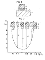
- the structure shown in FIG. 2 consists of a 300 nm thick n-doped (phosphorus or arsenic) polysilicon layer 3 and a 200 nm thick tantalum silicide layer 4 deposited on a silicon substrate 1 provided with a 20 nm thick SiO 2 layer 2.
- the photoresist layer used as an etching mask is designated by 5.
- the tantalum: silicon ratio is approximately 1: 2 (fluctuations in the Ta: Si ratio are permitted at 30% - 50% Ta).
- a structure is shown in FIG. 2 in which a strict anisotropic etching was desired. This can e.g.
- the switchover point from the first to the second stage can e.g. B. by recording the intensity of a suitable emission line of the plasma ..
- a very high selectivity poly-Si to SiO 2 of> 30: 1 can be achieved.
- FIG. 3 shows how the edge profiles of the double layer 3, 4 change with the composition of the etching gas mixture.
- the mixing ratio SF 6 : C1 2 is the abscissa and the etching time is the ordinate applied for the double layer.
- the dashed curve drawn in the figure shows the dependence of the etching time on the gas composition.
- Structure a shows a structure etched without chlorine components with a long etching time (see arrow a).
- Structure b has a very low etching time (see arrow b).
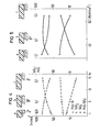
- FIGS. 4 and 5 show the etching speed in nm / min as a function of the gas pressure in Pa (FIG. 4) and the HF power in watts / cm 2 (FIG. 5).
- the arrows mark the conditions under which the structures shown were obtained.
- the arrows for the structures with the most favorable conditions are marked more strongly.
- an RF power of 0.1 W / cm was set.
- the x-dashed curve applies to tantalum silicide, the o-dashed curve for polysilicon, the 0-dashed curve for SiO 2 and the curve with S-dashed curve shows the selectivities of polysilicon: Si0 2 .
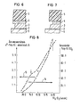
- FIGS. 6 and 7 It was found that, with a constant gas mixture, the etching profile also depends sensitively on the reactor geometry, that is to say on the ratio of active or plasma volume to the total volume of the reactor. The ratio influences the concentration distribution of the various radicals in the plasma. In the structure depicted in FIG. 6, the ratio of the active volume to the reactor volume was ⁇ 1:20, while in FIG. 7 the ratio was approximately 1: 2, that is to say the active volume corresponded to half the reactor volume. The main difference is that in the first case the silicide (the upper layer) etches anisotropically with respect to the photoresist mask in all SF 6 : Cl 2 ratios. In the second case, the silicide etching behavior can be varied from anisotropic to severe under-etching via the mixing ratio (see FIG. 3).
- Figure 8 If the polycide layer (3, 4) is to have local contact with the silicon substrate (buried contact), a certain etching of the substrate (1) cannot be avoided (see Figure 1, arrow 13). This can lead to increased contact resistances between the polycide and the substrate at the end of the circuit manufacturing process. With proper choice of the fluoro-chloro-ratio in the reaction gas can be relatively high (up to 10: 1) selectivity of n + - polysilicon: silicon - reach substrate and thus keep the etching of the substrate is very low. These relationships can be seen in FIG. 8.
- the curve marked with arrow 14 applies to the selectivity, that with arrow 15 applies to the etching speed ratio.
- the markings shown represent measuring points.
- the most favorable range for a gas mixture ratio SF 6 : Cl 2 is between 5:15 and 2:18.
- the silicide is made polycrystalline and of low resistance.
- the silicide / polysilicon layer interface is much more homogeneous, that is to say less rough than after the tempering. This has the advantage that the switchover point can be better defined when etching in a two-stage process.
Landscapes
- Drying Of Semiconductors (AREA)
- Electrodes Of Semiconductors (AREA)
- Internal Circuitry In Semiconductor Integrated Circuit Devices (AREA)
Applications Claiming Priority (2)
| Application Number | Priority Date | Filing Date | Title |
|---|---|---|---|
| DE3216823 | 1982-05-05 | ||
| DE19823216823 DE3216823A1 (de) | 1982-05-05 | 1982-05-05 | Verfahren zum herstellen von strukturen von aus metallsilizid und polysilizium bestehenden doppelschichten auf integrierte halbleiterschaltungen enthaltenden substraten durch reaktives ionenaetzen |
Publications (2)
| Publication Number | Publication Date |
|---|---|
| EP0094528A2 true EP0094528A2 (fr) | 1983-11-23 |
| EP0094528A3 EP0094528A3 (fr) | 1987-05-06 |
Family
ID=6162783
Family Applications (1)
| Application Number | Title | Priority Date | Filing Date |
|---|---|---|---|
| EP83104121A Withdrawn EP0094528A3 (fr) | 1982-05-05 | 1983-04-27 | Procédé pour la fabrication de structures à double couche comportant du silicide de métal et du polysilicium sur des substrats comportant des circuits intégrés par attaque chimique par ions réactifs |
Country Status (4)
| Country | Link |
|---|---|
| US (1) | US4473436A (fr) |
| EP (1) | EP0094528A3 (fr) |
| JP (1) | JPS58204538A (fr) |
| DE (1) | DE3216823A1 (fr) |
Cited By (3)
| Publication number | Priority date | Publication date | Assignee | Title |
|---|---|---|---|---|
| EP0126969A3 (en) * | 1983-04-29 | 1987-09-30 | Siemens Aktiengesellschaft Berlin Und Munchen | Process for manufacturing double-layer structures comprising metallic silicides, especially silicide-polysilicon, for integrated semiconductor circuits using reactive ion etching |
| EP0256311A3 (en) * | 1986-09-08 | 1990-07-25 | International Business Machines Corporation | Rie process for etching silicon isolation trenches and polycides with vertical surfaces |
| EP0516043A3 (en) * | 1991-05-29 | 1993-10-06 | Tokyo Electron Limited | Dry etching method |
Families Citing this family (28)
| Publication number | Priority date | Publication date | Assignee | Title |
|---|---|---|---|---|
| US4659426A (en) * | 1985-05-03 | 1987-04-21 | Texas Instruments Incorporated | Plasma etching of refractory metals and their silicides |
| US4624739A (en) * | 1985-08-09 | 1986-11-25 | International Business Machines Corporation | Process using dry etchant to avoid mask-and-etch cycle |
| US4734157A (en) * | 1985-08-27 | 1988-03-29 | International Business Machines Corporation | Selective and anisotropic dry etching |
| JPH0628290B2 (ja) * | 1985-10-09 | 1994-04-13 | 三菱電機株式会社 | 回路用ヒューズを備えた半導体装置 |
| US4713141A (en) * | 1986-09-22 | 1987-12-15 | Intel Corporation | Anisotropic plasma etching of tungsten |
| EP0272143B1 (fr) * | 1986-12-19 | 1999-03-17 | Applied Materials, Inc. | Procédé de décapage par bromine pour silicium |
| US4836886A (en) * | 1987-11-23 | 1989-06-06 | International Business Machines Corporation | Binary chlorofluorocarbon chemistry for plasma etching |
| USH596H (en) | 1988-02-16 | 1989-03-07 | The United States Of America As Represented By The Secretary Of The Army | Method of etching titanium diboride |
| JP2506151B2 (ja) * | 1988-06-15 | 1996-06-12 | シャープ株式会社 | 半導体装置の製造方法 |
| US4981816A (en) * | 1988-10-27 | 1991-01-01 | General Electric Company | MO/TI Contact to silicon |
| US5271799A (en) * | 1989-07-20 | 1993-12-21 | Micron Technology, Inc. | Anisotropic etch method |
| US5201993A (en) * | 1989-07-20 | 1993-04-13 | Micron Technology, Inc. | Anisotropic etch method |
| US5160408A (en) * | 1990-04-27 | 1992-11-03 | Micron Technology, Inc. | Method of isotropically dry etching a polysilicon containing runner with pulsed power |
| US5110411A (en) * | 1990-04-27 | 1992-05-05 | Micron Technology, Inc. | Method of isotropically dry etching a poly/WSix sandwich structure |
| KR0176715B1 (ko) * | 1990-07-30 | 1999-04-15 | 오가 노리오 | 드라이에칭방법 |
| US5094712A (en) * | 1990-10-09 | 1992-03-10 | Micron Technology, Inc. | One chamber in-situ etch process for oxide and conductive material |
| US5160407A (en) * | 1991-01-02 | 1992-11-03 | Applied Materials, Inc. | Low pressure anisotropic etch process for tantalum silicide or titanium silicide layer formed over polysilicon layer deposited on silicon oxide layer on semiconductor wafer |
| US5658425A (en) * | 1991-10-16 | 1997-08-19 | Lam Research Corporation | Method of etching contact openings with reduced removal rate of underlying electrically conductive titanium silicide layer |
| US5269879A (en) * | 1991-10-16 | 1993-12-14 | Lam Research Corporation | Method of etching vias without sputtering of underlying electrically conductive layer |
| US5354417A (en) * | 1993-10-13 | 1994-10-11 | Applied Materials, Inc. | Etching MoSi2 using SF6, HBr and O2 |
| JPH10270428A (ja) * | 1997-03-27 | 1998-10-09 | Mitsubishi Electric Corp | プラズマ処理装置 |
| JPH10270430A (ja) | 1997-03-27 | 1998-10-09 | Mitsubishi Electric Corp | プラズマ処理装置 |
| US5856239A (en) * | 1997-05-02 | 1999-01-05 | National Semiconductor Corporaton | Tungsten silicide/ tungsten polycide anisotropic dry etch process |
| JP3336975B2 (ja) * | 1998-03-27 | 2002-10-21 | 日本電気株式会社 | 基板処理方法 |
| US6074954A (en) | 1998-08-31 | 2000-06-13 | Applied Materials, Inc | Process for control of the shape of the etch front in the etching of polysilicon |
| KR100430950B1 (ko) * | 1998-09-01 | 2004-06-16 | 엘지.필립스 엘시디 주식회사 | 박막트랜지스터 및 그 제조방법 |
| DE10244862B4 (de) * | 2002-09-23 | 2006-09-14 | IHP GmbH - Innovations for High Performance Microelectronics/Institut für innovative Mikroelektronik | Verfahren zur Herstellung eines elektronischen Bauelements mit einer Praseodymoxid-Schicht |
| US20140199833A1 (en) * | 2013-01-11 | 2014-07-17 | Applied Materials, Inc. | Methods for performing a via reveal etching process for forming through-silicon vias in a substrate |
Family Cites Families (14)
| Publication number | Priority date | Publication date | Assignee | Title |
|---|---|---|---|---|
| JPS537549A (en) * | 1976-07-09 | 1978-01-24 | Mitsubishi Electric Corp | Etchant for dry etching |
| US4128670A (en) * | 1977-11-11 | 1978-12-05 | International Business Machines Corporation | Fabrication method for integrated circuits with polysilicon lines having low sheet resistance |
| US4203800A (en) * | 1977-12-30 | 1980-05-20 | International Business Machines Corporation | Reactive ion etching process for metals |
| US4211601A (en) * | 1978-07-31 | 1980-07-08 | Bell Telephone Laboratories, Incorporated | Device fabrication by plasma etching |
| US4214946A (en) * | 1979-02-21 | 1980-07-29 | International Business Machines Corporation | Selective reactive ion etching of polysilicon against SiO2 utilizing SF6 -Cl2 -inert gas etchant |
| JPS5626450A (en) * | 1979-08-13 | 1981-03-14 | Hitachi Ltd | Manufacture of semiconductor device |
| US4383885A (en) * | 1980-02-06 | 1983-05-17 | Bell Telephone Laboratories, Incorporated | Reactive sputter etching of polysilicon utilizing a chlorine etch gas |
| JPS5731140A (en) * | 1980-07-31 | 1982-02-19 | Toshiba Corp | Etching method by reactive ion |
| DE3045922A1 (de) * | 1980-12-05 | 1982-07-08 | Siemens AG, 1000 Berlin und 8000 München | Verfahren zum herstellen von strukturen von aus siliziden oder aus silizid-polysilizium bestehenden schichten durch reaktives sputteraetzen |
| DE3103177A1 (de) * | 1981-01-30 | 1982-08-26 | Siemens AG, 1000 Berlin und 8000 München | Verfahren zum herstellen von polysiliziumstrukturen bis in den 1 (my)m-bereich auf integrierte halbleiterschaltungen enthaltenden substraten durch plasmaaetzen |
| CA1202597A (fr) * | 1981-05-22 | 1986-04-01 | Jean S. Deslauriers | Procede d'application d'un revetement reactif au tantale et au silicium |
| US4384938A (en) * | 1982-05-03 | 1983-05-24 | International Business Machines Corporation | Reactive ion etching chamber |
| US4414057A (en) * | 1982-12-03 | 1983-11-08 | Inmos Corporation | Anisotropic silicide etching process |
| US4411734A (en) * | 1982-12-09 | 1983-10-25 | Rca Corporation | Etching of tantalum silicide/doped polysilicon structures |
-
1982
- 1982-05-05 DE DE19823216823 patent/DE3216823A1/de not_active Withdrawn
-
1983
- 1983-04-27 EP EP83104121A patent/EP0094528A3/fr not_active Withdrawn
- 1983-05-02 JP JP58078103A patent/JPS58204538A/ja active Pending
- 1983-05-02 US US06/490,481 patent/US4473436A/en not_active Expired - Lifetime
Cited By (3)
| Publication number | Priority date | Publication date | Assignee | Title |
|---|---|---|---|---|
| EP0126969A3 (en) * | 1983-04-29 | 1987-09-30 | Siemens Aktiengesellschaft Berlin Und Munchen | Process for manufacturing double-layer structures comprising metallic silicides, especially silicide-polysilicon, for integrated semiconductor circuits using reactive ion etching |
| EP0256311A3 (en) * | 1986-09-08 | 1990-07-25 | International Business Machines Corporation | Rie process for etching silicon isolation trenches and polycides with vertical surfaces |
| EP0516043A3 (en) * | 1991-05-29 | 1993-10-06 | Tokyo Electron Limited | Dry etching method |
Also Published As
| Publication number | Publication date |
|---|---|
| DE3216823A1 (de) | 1983-11-10 |
| US4473436A (en) | 1984-09-25 |
| JPS58204538A (ja) | 1983-11-29 |
| EP0094528A3 (fr) | 1987-05-06 |
Similar Documents
| Publication | Publication Date | Title |
|---|---|---|
| DE3216823A1 (de) | Verfahren zum herstellen von strukturen von aus metallsilizid und polysilizium bestehenden doppelschichten auf integrierte halbleiterschaltungen enthaltenden substraten durch reaktives ionenaetzen | |
| EP0000897B1 (fr) | Procédé de fabrication de régions de silicium isolées latéralement | |
| EP0015403B1 (fr) | Procédé de décapage de silicium par ions réactifs | |
| EP0010624B1 (fr) | Procédé pour la réalisation d'ouvertures de masque très petites pour la fabrication de circuits intégrés à semiconducteurs | |
| DE69033615T2 (de) | Ätzen von Kontaktlöchern in einer dielektrischen Doppelschicht mit einer einzigen Ätzkammer | |
| DE3841588C2 (fr) | ||
| DE68927699T2 (de) | Trockenätzverfahren | |
| DE69025300T2 (de) | Integrierte Schaltung mit einer planarisierten dielektrischen Schicht | |
| DE3856022T2 (de) | Selektives Ätzen dünner Schichten | |
| DE10016340C1 (de) | Verfahren zur Herstellung von flaschenförmigen Tiefgräben zur Verwendung in Halbleitervorrichtungen | |
| DE3231987C2 (de) | Verfahren zur Herstellung einer Cobaltsilicidschicht in einem Halbleiterbauelement | |
| DE69724192T2 (de) | Verfahren zum Ätzen von Polyzidstrukturen | |
| DE69616981T2 (de) | Verfahren zur ätzung eines polysiliziummusters | |
| DE69126149T2 (de) | Trockenätzverfahren | |
| DE68923305T2 (de) | Elektrische Leitungen für elektronische Bauelemente. | |
| DE3706127C2 (fr) | ||
| DE10127622B4 (de) | Verfahren zur Herstellung eines mit HDPCVD-Oxid gefüllten Isolationsgrabens | |
| DE69409347T2 (de) | Verfahren zum Herstellen von Halbleitervorrichtungen | |
| DE2930293A1 (de) | Aetzverfahren bei der herstellung eines gegenstandes | |
| DE3245276A1 (de) | Verfahren zum ausbilden von submikrometer-merkmalen in halbleiterbauelementen | |
| DE3873903T2 (de) | Verfahren, um eine elektrische verbindung auf einer silizium-halbleitervorrichtung herzustellen. | |
| DE3211761A1 (de) | Verfahren zum herstellen von integrierten mos-feldeffekttransistorschaltungen in siliziumgate-technologie mit silizid beschichteten diffusionsgebieten als niederohmige leiterbahnen | |
| EP0126969B1 (fr) | Procédé pour la formation de structures comportant des siliciures métalliques, en particulier en siliciure polysilicium, pour circuits intégrés à semi-conducteurs par attaque par ions réactifs | |
| DE69130787T2 (de) | Ätzverfahren für eine leitende Doppelschicht-Struktur | |
| DE10002121B4 (de) | Herstellung einer Halbleitervorrichtung mit flachen Sperrschichten |
Legal Events
| Date | Code | Title | Description |
|---|---|---|---|
| PUAI | Public reference made under article 153(3) epc to a published international application that has entered the european phase |
Free format text: ORIGINAL CODE: 0009012 |
|
| AK | Designated contracting states |
Designated state(s): DE FR GB |
|
| 17P | Request for examination filed |
Effective date: 19841119 |
|
| PUAL | Search report despatched |
Free format text: ORIGINAL CODE: 0009013 |
|
| AK | Designated contracting states |
Kind code of ref document: A3 Designated state(s): DE FR GB |
|
| 17Q | First examination report despatched |
Effective date: 19891129 |
|
| STAA | Information on the status of an ep patent application or granted ep patent |
Free format text: STATUS: THE APPLICATION HAS BEEN WITHDRAWN |
|
| 18W | Application withdrawn |
Withdrawal date: 19901212 |
|
| RIN1 | Information on inventor provided before grant (corrected) |
Inventor name: BEINVOGL, WILLY, DR. |