EP0313278A2 - Defektkompensation für Festkörperkameras - Google Patents
Defektkompensation für Festkörperkameras Download PDFInfo
- Publication number
- EP0313278A2 EP0313278A2 EP88309656A EP88309656A EP0313278A2 EP 0313278 A2 EP0313278 A2 EP 0313278A2 EP 88309656 A EP88309656 A EP 88309656A EP 88309656 A EP88309656 A EP 88309656A EP 0313278 A2 EP0313278 A2 EP 0313278A2
- Authority
- EP
- European Patent Office
- Prior art keywords
- defect
- data
- compensating
- signal
- image pickup
- Prior art date
- Legal status (The legal status is an assumption and is not a legal conclusion. Google has not performed a legal analysis and makes no representation as to the accuracy of the status listed.)
- Granted
Links
Images



Classifications
-
- H—ELECTRICITY
- H04—ELECTRIC COMMUNICATION TECHNIQUE
- H04N—PICTORIAL COMMUNICATION, e.g. TELEVISION
- H04N23/00—Cameras or camera modules comprising electronic image sensors; Control thereof
- H04N23/60—Control of cameras or camera modules
- H04N23/667—Camera operation mode switching, e.g. between still and video, sport and normal or high- and low-resolution modes
-
- H—ELECTRICITY
- H04—ELECTRIC COMMUNICATION TECHNIQUE
- H04N—PICTORIAL COMMUNICATION, e.g. TELEVISION
- H04N25/00—Circuitry of solid-state image sensors [SSIS]; Control thereof
- H04N25/60—Noise processing, e.g. detecting, correcting, reducing or removing noise
- H04N25/68—Noise processing, e.g. detecting, correcting, reducing or removing noise applied to defects
- H04N25/69—SSIS comprising testing or correcting structures for circuits other than pixel cells
Definitions
- This invention relates to solid state image pickup apparatus or solid-state television cameras.
- an image pickup output is obtained at the solid state image pickup device in a field readout mode, in which signal charges are read out from the totality of the picture elements or pixels during one field period, or in a frame readout mode, in which the signal charges are read out from the totality of the pixels during one frame period.
- an electronic shutter function provided by controlling the effective charge accumulation time of the solid state image pickup device is added or incorporated in place of a mechanical shutter system.
- the image pickup unit of a solid state colour image pickup apparatus for picking up a colour image is so designed that the image pickup is performed by three solid state image pickup devices, in such a manner that colour video signals are formed by image pickup outputs of images of a scene in three primary colours formed by picked up image light which has been colour-separated into three primary colours, namely red (R), green (G) and blue (B).
- a so-called space pixel shifting system has been proposed as a means for increasing the resolution in the horizontal direction in the solid-state colour image pickup apparatus for imaging a scene or an object for each of the colour components obtained upon colour separation of the image light.
- a solid-state image pickup device for example the solid-state image pickup device for imaging the green (G) colour component of a scene, is arranged at a position shifted by one half of a pixel pitch in the horizontal direction with respect to the solid-state image pickup devices for imaging the red (R) and blue (B) colour components of the scene.
- the memory capacity can be reduced by encoding and storing the distance between defective pixels, the memory is in perpetual operation, resulting in an increase in wasteful power consumption and an increase in the power consumption of the image pickup apparatus as a whole.
- the above-described interpolating compensation technique leads to increased compensation error should there be no correlation in the image pickup output obtained at the pixel lying close to the defective pixel.
- defect compensation is carried out only for image defects caused by white flaw image defects having a high defect level.
- an image defect caused by a white flaw defective pixel appears rather conspicuous, but at an extremely low level at ambient temperature, so that it may be safely disregarded as a defect.
- the image defect increases exponentially with a rise in temperature.
- the compensation signal needs to be compensated further for temperature.
- the white flaw defect may be over-compensated or under-compensated such that so-called compensation flaws remain in the compensated image pickup output.
- the charge accumulation time of the solid state imaging device of the image pickup unit is variably controlled by the preset speed of the electronic shutter, with the result that the defect level due to a defective pixel included in the image pickup output from the defective pixel is changed.
- the defect level is also changed by switching of the readout modes of the signal charges.
- the charge accumulation time be set to 1/2 in, for example, the field readout mode, the signal charges produced are equal to one half those for the normal mode.
- the effective charge accumulation time is one quarter of the normal accumulation time.
- the data concerning the positions of the defective pixels included in the solid-state image pickup device are stored in the memory and the compensation for defects effected on the basis of data read out from the memory, compensation for defects can be made very satisfactorily without concomitant compensation errors.
- the volume of the data is undesirably increased since the data concerning the location of the defective pixels and the level of the defective components included in the output signal needs to be stored in the memory.
- the location of each of the defective pixels is indicated by an absolute address
- the number of bits used as position data for each defective pixel is increased when employing a solid state image pickup device having an increased number of pixels to increase the high image resolution, so that the memory capacity needs to be correspondingly increased.
- a solid state television camera comprising: solid state image sensor means of semiconductor material for providing an output signal corresponding to an image of an object, the image sensor means including picture elements arranged in a raster having parallel scanning lines which are, in turn, arranged in order in a direction orthogonal to the direction of said scanning lines, said semiconductor material having crystal defects at locations of a plurality of said picture elements which will create noise at corresponding times in said output signal; memory means for memorising position data corresponding to the positions of said crystal defects in the semiconductor material and defect level data corresponding to the level of a compensating signal for compensating the output signal associated with each of said defect locations, said defect level data being measured at a higher temperature than a normal operating temperature; readout means for reading out said position data and said defect level data from the memory means; temperature sensing means for sensing the temperature around the solid state image sensor means; compensating signal generating means connected to be supplied with said position data and defect level data and operative to generate the compensating signal at the timing at which said crystal defect is scanned and
- the solid state image sensor means which may, for example, comprise a charge coupled device (CCD)
- CCD charge coupled device
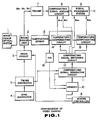
- FIG 1 is a block diagram of a colour video camera embodying the invention in which colour image pickup is achieved at a three-plate type image pickup unit 2 constituted by three solid-state image sensors in the form of separate plates, on image pick-up surfaces of which are formed images of a scene derived from picked up image light colour- separated by an image pickup unit 1 into three primary colours, namely red (R), green (G) and blue (B).
- a three-plate type image pickup unit 2 constituted by three solid-state image sensors in the form of separate plates, on image pick-up surfaces of which are formed images of a scene derived from picked up image light colour- separated by an image pickup unit 1 into three primary colours, namely red (R), green (G) and blue (B).
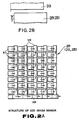
- the solid-state image sensors constituting the image pickup unit 2 are, for example, formed, as shown in Figure 2A, by a large number of light-receiving sections S each associated with one of a plurality of pixels arranged in a matrix, vertical transfer registers VR provided along vertical directions on one side of the light receiving sections S, and a horizontal transfer register HR provided at terminal ends of the vertical transfer registers VR.
- Three interline transfer type CCD image sensors 2R, 2G and 2B are used, in each of which signal charges corresponding to the light intensities received at each of the sections S are transferred to associated vertical transfer registers VR corresponding to associated vertical lines at intervals of one field period or one frame period, and the signal charges are then transferred through the vertical transfer registers VR to the horizontal transfer register HR, from which the signal charges for each horizontal line are taken out as an image pickup output.
- the image pickup unit 2 is arranged and constructed in accordance with a spatial pixel shift system in such a manner that the CCD image sensor 2G for picking up the image of the green (G) component of the scene is shifted by 1/2 pixel pitch (P/2) in the horizontal direction with respect to the other two CCD image sensors 2R and 2B for picking up the images of the field of the red (R) and blue (B) components, respectively.
- a spatial pixel shift system in such a manner that the CCD image sensor 2G for picking up the image of the green (G) component of the scene is shifted by 1/2 pixel pitch (P/2) in the horizontal direction with respect to the other two CCD image sensors 2R and 2B for picking up the images of the field of the red (R) and blue (B) components, respectively.
- a drive circuit 3 for the image pickup unit 2 receives from a timing generator 5 a horizontal transfer pulse signal ⁇ H and a vertical transfer pulse signal ⁇ v synchronised with sync signals SYNC produced by a sync generator 4.
- a system controller 6 transmits to the drive circuit 3: a read mode designating signal designating a field read mode for reading the signal charges corresponding to the amount of received light obtained at each of the light receiving sections S of the CCD image sensors 2R, 2G and 2B, in their entirety, during one field period, and a frame read mode designating a frame read mode for reading the signal charges obtained at the light receiving sections S in their entirety during one frame period; and a shutter control signal for controlling the charge accumulating time for the CCD image sensors to control the shutter speed of a so-called electronic shutter.
- the frame readout mode has a charge accumulation time of 1/30 of a second and the field read mode has a charge accumulation time of 1/60 of a second, namely half that for the frame read mode.
- the signal charges obtained at two vertically adjoining light receiving sections S are summed together before being read so as to provide the same sensitivity as that during the frame read mode.
- Colour image pickup outputs SR, SG and SB obtained at the image pickup unit 2 constituted by the three CCD image sensors 2R, 2G and 2B are supplied through a preamplifier 7 and a compensating signal adding circuit 8 to a signal processing system 9.
- the pickup outputs SR, SG and SB are subjected to defect compensation in the adding circuit 8 and to processing including gamma or shading compensation in the processing system 9, so as to be then outputted after conversion into video signals conforming to a standard television system prescribed by the CCIR or EIA.
- the CCD image sensors 2R, 2G and 2B are previously subjected to defect tests analysing the location of defective pixels, and the kind of as well as the level of the defects, data corresponding thereto being stored in a memory 10 as compensating data.
- White flaw defect compensation signals WCP, black flaw defect compensation signals BCP, white shading compensation signals WSH and black shading compensation signals BSH are formed at the timing of the output signals of the defective pixels of the CCD image sensors 2R, 2G and 2B, on the basis of the compensation data read from the memory 10, by a compensating signal generator circuit 11.
- the compensation signals WCP, BCP, WSH and BSH are supplied through a compensating signal switching circuit 12 to the compensating signal adding circuit 8 and to the signal processing system 9 for compensating for image defects in the compensating signal adding circuit 8 and the signal processing system 9.
- the image pickup unit 2 is provided with a temperature sensor 13 for sensing the temperatures of the CCD image sensors 2R, 2G and 2B so that the compensating signals WCP and BSH for the white flaws and black shading, the defect level of which exhibits temperature dependency, will be compensated for temperature in temperature compensating circuits 14 and 15 on the basis of the detection output of the temperature sensor 13.
- the temperatures of the CCD image sensors 2R, 2G and 2B, as indicated by the detection output of the temperature sensor 13, are digitised in an analog to digital (A/D) converter 16 so as to be then transmitted as address data to the memory 10.
- A/D analog to digital
- the defect tests of the CCD image sensors 2R, 2G and 2B are carried out at a test temperature which is higher than the ambient temperature at which the image defects are expected to take place frequently.
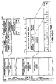
- the defect tests are carried out in such a manner that the locations A1, A2, ... of the white and black flaw defect pixels of the CCD image sensors 2R, 2G and 2B are identified, the kinds and the levels l1, l2, ... of the defects are detected, and the positional data of the defective pixels are obtained in the following way. That is, referring to Figure 3, the first defect pixel position A1, counting from a reference point A0, is represented by digital data of a predetermined number of bits corresponding to the distance d1 from the reference point A0 to an encoded form.
- the position An of another given defective pixel is represented by digital data of a predetermined number of bits corresponding to the distance dn from the preceding defective pixel position A(n-1).
- n is any arbitrary integer
- the relative distance between any arbitrary defective pixel and the next defective pixel is so long that it cannot be represented by digital data of the predetermined number of bits, as in the case of a dummy pixel position ADM1 between a first defective pixel position A1 and a second defective pixel position A2 having a relative distance d as shown for example in Figure 3, a dummy defective pixel is set between these defective pixels so that the relative distance d is divided into a distance d2 from the first defective pixel position A1 to the dummy defective pixel position ADM1 and a distance d3 from the dummy defective pixel position ADM1 to the second defective pixel position A2, the distances d2 and d3 being represented by digital data having respective predetermined number of bits.
- the positions A1, A2, ... of the defective pixels of the CCD image sensors 2R, 2G and 2B are represented by two-dimensional absolute addresses, 10 data bits each along the horizontal direction and along the vertical direction, a total of 20 data bits are needed for the address data.
- the defective pixel position An where n is any arbitrary integer, is represented by the encoded digital data of a predetermined number of bits corresponding to the distance dn from the immediately preceding defective pixel position A(n-1) in accordance with a relative address system
- the address data can be compressed to the number of bits necessary to represent the maximum value of the relative address. For example, for relative address data of 12 bits, data compression of 8 bits may be achieved for one defective pixel position.
- one or more dummy defective pixel positions ADM may be set between the defective pixel positions An and A(n+1), so that the relative distance dn is divided and reduced to not more than 4.5 lines, such that the defective pixel position A(n+1) is represented by 12 bits of the relative address data.
- one or more dummy defective pixels may be set between the defective pixels for dividing the relative distance dn in such a manner that the totality of the defective pixel positions can be represented by the digital data of the predetermined number of bits.
- the image pickup output signals are not affected in quality by the dummy defective pixel positions ADM1 by setting the dummy defective pixel positions so as to lie within the blanking period BLK of the image pickup output signals read out from the CCD image sensors 2R, 2G and 2B.
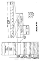
- the memory 10 is divided into a field readout area ARFD from an address 0 to an address 4095 and a frame readout area ARFM from an address 4096 to an address 8191, as shown in the memory map of Figure 4.
- Each of the readout areas ARFD and ARFM is divided into a minimum compensating amplitude data area ARSA, a compensating data area ARCM and a shutter speed data area ARSS.
- minimum compensating amplitude data area ARSA there are written a number N of minimum compensating amplitude data DSA indicating the minimum amplitude at which it is necessary to perform compensation, in dependence upon the image pickup conditions, such as the temperatures and the shutter speed, on the image pickup outputs of the CCD image sensors 2R, 2G and 2B.
- the minimum amplitude data DSA is formed by 2-byte data, of which 4 bits are allotted to each of the minimum compensating channel amplitude data DSAR, DSAG, and DSAB for the R, G and B channels, 2 bits are allotted to cycle time data and the remaining 2 bits are unused.
- the data DCM are made up of 8-bit amplitude data DCMA associated with the defect level, 2-bit mode select data DMS indicating the kind of defect, 2-bit colour code data DCC indicating the channel to be compensated, and 3-byte data formed by the 12-bit relative address data RADR indicating the distance to the next defect pixel position.
- the data DCM include data DCM′ concerning the dummy defective pixels.
- the shutter speed data area ARSS there are written 15 2-byte data each composed of shutter data SHD for converting 4-bit shutter speed data indicating the present shutter speed of the electronic shutter into 3-bit data and 12-bit first address data FADR indicating the start address of the above data area ARCM, that is the address 2N.
- the compensating signal generator circuit 11 comprises first to seventh latch circuits 21 to 27, to which various data read out from the memory 10 are supplied, and a strobe generator circuit 28.
- the circuits 21 to 28 are shown in Figure 5, which shows an example of the compensating signal generator circuit 11, together with peripheral circuits for the circuit 11.
- the compensating signal generator circuit 11 When performing the image pickup operation at the operating mode preset in the system controller, the compensating signal generator circuit 11 performs an initialising operation during the blanking periods at a one field or one frame interval in such a manner that, depending upon the image pick-up conditions, such as the shutter speed preset in the system controller 6 or the temperature data transmitted from the temperature sensor 13 by way of the A/D converter 16, the minimum amplitude data DSAR, DSAG and DSAB for the R, G and B channels read out from the minimum amplitude data area ARSA of the memory 10 are latched in the first to third latch circuits 21, 22 and 23 and the shutter data SHD read out from the shutter speed data area ARSS of the memory 10 are latched in the fourth latch circuit 24.
- the image pick-up conditions such as the shutter speed preset in the system controller 6 or the temperature data transmitted from the temperature sensor 13 by way of the A/D converter 16
- the generator circuit 11 also operates, on the basis of the first address data FADR read out from the shutter speed data area ARSS, in such a fashion that the strobe generator circuit 28 causes an address counter 40 to read out data DCM1 from the leading address in the data area ARCM of the memory 10, that is the address 2N and the relative address data RADR indicating the distance from the point of origin A0 to the first defective pixel position A1 is latched in the strobe generator circuit 28 while the amplitude data DCMA, colour code data DCC and the mode select data DMS are latched in the fifth to seventh latch circuits 25 to 27.
- the strobe generator circuit 28 When the strobe generator 28 terminates the above-described initialising operation and proceeds to the compensating operation, the strobe generator circuit 28 outputs a strobe pulse at the timing of the first defective pixel position on the basis of the relative address data RADR latched in the course of the initialising operation to increment the address counter 40 to read out the next data DCM2 from the data area ARCM of the memory 10 to latch the relative address data indicating the distance to the next defective pixel position A1 in the strobe generator 28, as well as to latch the amplitude data DCMA, colour code data DCC and mode select data DMS in the fifth to seventh latch circuits 25 to 27 and to output the strobe pulses sequentially at the timing of the respective defective pixel positions An.
- the first to third latch circuits 21 to 23 latch the minimum amplitude data DSAR, DSAG and DSAB of the R, G and B channels read out from the minimum amplitude data area ARSA of the memory 10, these amplitude data DSAR, DSAG and DSAB then being transmitted through a selector 29 to a comparator 30.
- the fourth latch circuit 24 latches the shutter data SHD read out from the shutter speed data area ARSS of the memory 10, which shutter speed data are then transmitted to a bit shift circuit 31 as control data.
- the fifth to seventh latch circuits 25, 26 and 27 are operative to latch amplitude data DCMA, colour code data DCC and mode select data DMS included in the data DCM readout from the data area ARCM of the memory 10.
- the amplitude data latched in the fifth latch circuit 25 are transmitted to the comparator 30, and also to a first switching circuit 32 (both directly and through the bit shift circuit 31) and thence to a digital/analog (D/A) converter 33.
- the colour code data DCC latched in the sixth latch circuit 26 are supplied to the selector 29 as control data, while being simultaneously transmitted as control data to a first decoder 43 as described below.
- the mode select data DMS latched in the seventh circuit 27 are transmitted as control data to the first switching circuit 32, while being simultaneously transmitted as control data to a second switching circuit 41 and a second decoder 47 as described below.
- the selector 29 selects that one of the minimum amplitude data DSAR, DSAG and DSAB for the R, G and B channels latched in the first to third latch circuits 21 to 23 that is designated by the colour code data DCC supplied as control data from the sixth latch circuit 26 and transmits the selected minimum amplitude data DSA to the comparator 30.
- the comparator 30 compares the minimum amplitude data DSA selected by the selector 29 with the amplitude data DCMA latched in the fifth latch circuit 25 and transmits a comparison output signal to a third switching circuit 42 as control data.
- the third switching circuit 42 is closed when the amplitude data DCMA is larger than the minimum amplitude data DSA.
- the amplitude data DCMA transmitted from the fifth latch circuit 25 is subjected to a bit shifting operation, for example as shown in Table 1, in the bit shifting circuit 31.
- Table 1 Bit Shifting Operation shutter speed shutter data number of bits shifted gain 1/60 LLL 0 1 1/100 LLH 1 1/2 1/125 LLH 1 1/2 1/250 LHL 2 1/4 1/500 LHH 3 1/8 1/1000 HLL 4 1/16 1/2000 HLH 5 1/32 1/4000 HHL 6 1/64 1/10000 HHH 7 1/128
- the bit-shifted amplitude data DCMA are then transmitted by way of the first switching circuit 32 to the D/A converter 34.
- the first switching circuit 32 is controlled by the mode select data DMS, supplied from the seventh latch circuit 27 as control data, in such a manner as to select the bit shift circuit 31 when the mode select data DMS indicates the white flaw defect mode and to select the fifth latch circuit 25 when the mode select data indicates some other defect mode.
- the amplitude data transmitted by way of the first switching circuit 32 are converted in the D/A converter 33 into corresponding analog signals.
- the analog amplitude signals produced by the D/A converter 33 are supplied to first and second level adjustment circuits 34 and 35 and to the first and second temperature compensating circuits 14 and 15, so as to be selectively outputted by way of first to fourth signal switching circuits 36 to 39 from the circuits 34, 35, 14 and 15 as various amplitude compensating signals.
- the strobe generator circuit 28 On the basis of first address data FADR read out from the shutter speed data area ARSS of the memory 10 and the relative address data included in the data DCM read out from the data area ARCM of the memory 10, the strobe generator circuit 28 generates strobe pulses at timings associated with the defective pixel positions A1, A2, ... of the CCD image sensors 2R, 2G and 2B making up the image pickup unit 2, while simultaneously presetting the first address data and the relative address data in the address counter 40 of the memory 10.
- the second switching circuit 41 is controlled by the mode select data DMS, transmitted from the seventh latch circuit 27 as control data, in such a manner as to select the third switching circuit 42 when the mode select data DMS indicates the white flaw defect mode and to select the first decoder 43 when the mode select data indicates some other defect mode.
- the strobe pulse of the white flaw defect mode is transmitted through the third switching circuit 42 to the first decoder 43, while the strobe pulse of some other defect mode is transmitted directly to the first decoder 43.
- the third switching circuit 42 is controlled by the output of the comparator 30 as control data, in such a manner that the strobe pulse of the white flaw defect mode transmitted through the second switching circuit 41 is transmitted to the first decoder 43 only when the amplitude data latched at the fifth latch circuit 25 is larger than the minimum amplitude data DSA selected at the selector 29.
- the first decoder 43 transmits the strobe pulse to the second decoder 47 through D-type flip-flops 44, 45, 46 of one or all of the R, G and B channels selectively designated as shown in Table 2 by the 2-bit colour code data DCC supplied as control data from the sixth latch circuit 26.
- Clock input terminals of the D-type flip-flops 44 to 46 are supplied, from the timing generator 5, with clock pulse signals ⁇ R, ⁇ G and ⁇ B matched to the phase of each of the R, G and B channels, that is each of the colour components of the pickup output produced by the CCD image sensors 2R, 2G and 2B, for effecting phase matching of the strobe pulse signal supplied from the first decoder 43 by the clock pulse signals ⁇ R, ⁇ G and ⁇ B.
- the clock pulse signal ⁇ G for the G-channel is of opposite phase to the clock pulse signals ⁇ R and ⁇ B of the other (R and B) channels, so as to produce a strobe pulse signal matched to the phase of each of the R, G and B signals or colour components of the image pickup output obtained at each of the CCD sensors 2R, 2G and 2B of the image pickup unit 2.
- the second decoder 47 forms selective control data from this strobe pulse signal in association with the modes designated as shown in Table 3 by the 2-bit mode select data DMS transmitted as control data from the seventh latch circuit 27, and transmits the selective control data to the control input terminal of each of the first to fourth switching circuits 36 to 39.
- the analog amplitude signals outputted from the D/A converter 33 by way of the first or second level adjustment circuits 34, 35 or the first or second temperature compensating circuits 14, 15 are switched by the first to fourth signal switching circuits 36 to 39 in accordance with the selective control data from the second decoder 47 in the following manner, so as then to be outputted as the various compensating signals.
- the third switching circuit 38 selectively outputs to one of the R, G and B channels indicated by the colour code data DCC the analog amplitude signals outputted from the D/A converter 33 through the first temperature compensating circuit 14, as the white flaw defect compensating signal WCP.
- the mode select data DMS is LH, thus indicating the black flaw defect mode
- the first signal switching circuit 36 selectively outputs to one of the R, G and B channels indicated by the colour code data DCC the analog amplitude signals outputted from the D/A converter 33 by way of the first level adjustment circuit 34, as the black flaw defect compensating signal BCP.
- the fourth signal switching circuit 39 selectively outputs to one of the R, G and B channels indicated by the colour code data DCC the analog amplitude signals outputted from the D/A converter 33 by way of the second temperature compensating circuit 15, as the black shading compensating signal BSH.
- the second signal switching circuit 37 selectively outputs to one of the R, G and B channels indicated by the colour code data DCC the analog amplitude signal outputted from the D/A converter 33 through the second level adjustment circuit 35, as the white shading compensating signal WSH.
- the power supplied to the memory 10 is cut off or reduced, for power saving, except during a period or internal TR ( Figure 6) of several tens of clock periods before and after the read-out timing for the signal charges from each of the defective pixels of the CCD image sensors 2R, 2G and 2B making up the image pickup unit 2, that is a read-out timing tR of the data DCM.
- This previous wasteful power consumption by the memory 10 so as to realise power saving.
- the white flaw defect compensating signal WCP and the black flaw defect compensating signal BCP obtained upon selective switching of the analog amplitude signal outputted from the D/A converter 33 by the first and third switching circuits 36, 38 of the compensation signal switching circuit 12 at the timing of the defective pixel positions A1, A2, ...
- the decoded output of the second decoder 47 receiving the phase-matched strobe pulse signals at the D-type flip-flops 44 to 46 as selective control data are summed at the compensating signal adding circuit 8 in such a manner that the colour image pickup outputs SR, SG and SB of the R, G and B channels obtained at the image pickup unit 2, arranged in accordance with the spatial pixel shifting system, are subjected to a compensating operation for the image defects due to white and black flaw defects.
- the white flaw defect compensating signal WCP selected by the first compensating signal switching circuit 36 is summed at the compensating signal adding circuit 8 with the image pickup output obtained at the image pickup unit 2, after the amplitude lW of the analog amplitude signal supplied from the D/A converter 33 has undergone temperature compensation in the first temperature compensating circuit 14, to which is supplied the detection output of the temperature sensor 13 for detecting the temperature of each of the CCD image sensors 2R, 2G and 2B of the image pickup unit 2, as shown in Figure 7, whereby the amplitude is set to a new amplitude lW′ for optimum adjustment of the white flaw defect at the working temperature under the actual image pickup state, in such a manner as to perform an optimum adjustment of the white flaw defect exhibiting temperature dependency.
- the defect level of the white flaw defect exhibiting temperature dependency is extremely small at ambient temperature and may be safely disregarded as a defect, while it increases exponentially with an increase in temperature. Therefore, should there be a compensation error in the first temperature compensating circuit 14, which performs temperature compensation of the white flaw defect compensating signal WCP, the white flaw defect is over-compensated or under-compensated by the white flaw defect compensation signal WCP, so that a so-called compensation flaw remains in the image pickup output obtained after defect compensation.
- the minimum amplitude data DSA read out from the minimum amplitude data area ARSA of the memory 10 are latched in the first to third latch circuits 21 to 23 of the compensating signal generator circuit 11 in the course of the initialising operation, with the data such as the shutter speed or the operating temperature as the address data, in such a manner that compensation is not performed in the case of a white flaw defect having a low defect level (when the amplitude data DCMA read out from the data area ARCM of the memory 10 in the course of the actual image pickup operation is less then the minimum amplitude data DSA), in which event the problem of compensation flaw caused by white flaw defect compensation is most likely to occur, and only white flaw defects having a higher defect level are selectively compensated in order to provide for a more effective white flaw defect compensating operation.
- the signal level of the white flaw defect signal contained in the image pickup output is changed in dependence upon the charge accumulation time, that is the shutter speed.
- the amplitude data DCMA are subjected to the above-described bit shifting operation shown in Table 1 by the bit shift circuit 31 in the course of the image pickup operation on the basis of the shutter data latched in the fourth latch circuit 24 of the compensating signal generator circuit 11 in the course of the initialising operation, in such a manner that the preset shutter speed is associated with the gain of the white flaw defect compensating signal WCP to provide for an optimum white flaw defect compensating operation at all times.
- the field readout area ARFD and the frame readout area ARFM are provided in the memory 10 where the minimum amplitude data DSA, data DCM or the shutter data SHD for these readout modes are written previously. Data are read out from one of the field readout area ARFD and the frame readout area ARFM corresponding to the actually selected readout mode to perform the above-described initialising operation and compensating operation to provide for optimum defect compensation for any of the readout modes.
- the image pickup output compensated for image defects due to white and black flaw defects as described above, is subjected to shading compensation using black shading compensating signals BSH and white shading compensating signals WSH obtained upon selectively switching analog signals outputted from the D/A converter 33, as a function of the kind of the defect mode, by the second and fourth switching circuits 36 and 38 of the compensating signal switching circuit 12, under control of the signal processing system 9.
- the amplitude of the analog amplitude signal outputted by the D/A converter 33 is subjected to temperature compensation by the second temperature compensating circuit 15 to which the sensed output of the temperature sensor 13 is supplied, so that the black shading can be compensated to a minimum value at the operating temperature under the actual image pickup operating conditions with the aid of the black shading compensating signal BSH selected by the fourth signal switching circuit 39.
- the amplitude data included in the compensation data DCM read out from the memory 10 are selectively subjected to the above-described bit shifting operation, and the analog amplitude signals obtained by converting the amplitude data DCMA into analog form are selected by subjection to a temperature compensating operation. Then, using, as timing information, the control data obtained by decoding the strobe pulse signal formed on the basis of the relative address data RADR by the colour code data DCC or the mode select data DMS, the analog amplitude signals are switched by the signal switching circuit 12.
- defect compensation signals matched in phase to the image pickup outputs from the CCD image sensors 2R, 2G and 2B constituting the image pickup unit 2 and arranged and constructed in accordance with the spatial pixel shifting system, are formed and used to effect an optimum compensation of image defects due to white or black flaw defects of the CCD image sensors 2R, 2G and 2B, so that image pickup output signals having an extremely high picture quality are provided.
- the above-described embodiment of the invention has the following advantageous features. It provides a solid-state image pickup apparatus in which, in view of the above-described various inconveniences of the previously proposed solid state image pickup apparatus, the degraded picture quality ascribable to the image pickup output from defective pixels included in the solid state image pickup device, such as CCD devices, formed by semiconductor material, is compensated for by signal processing, in such a manner as to produce image pickup output signals having a superior picture quality.
- Timing information representing the defective pixel positions and amplitude information representing the level of defective components in the solid-state image pickup devices constituting the image pickup unit are separately processed by a double route processing system to form defect compensation signals, whereby the defect compensating operation may be performed positively so that changes in the various defect levels may be taken into account.
- Both image defects due to white flaw defect pixels having temperature dependency and the image defects due to black flaw defect pixels not having temperature dependency are compensated, in such a manner as to produce image pickup output signals having a superior picture quality. Even when the mode of reading out signal charges from the solid state image pickup devices constituting the image pickup unit is switched by a switching operation, defect compensation signals associated with the various operating modes can be formed in a simple manner to allow for a positive defect compensating processing of the solid-state image pickup devices.
- the charge accumulation time in each pixel can be preset variably, whereby, even when the charge accumulation time in the solid state image pickup devices is changed, a correct defect compensating operation may be performed in such a manner as to produce image output signals having a superior picture quality.
- the positions of defective pixels included in the solid state image pickup devices are indicated efficiently by position data formed by a smaller number of bits to simplify the construction of the memory means and the peripheral circuits to allow for an efficient compensating operation of image defects so as to provide image pickup output signals having a superior picture quality.
- the relative distance between the defective pixels in an encoded form is used as the position data for the defective pixels included in the solid state image pickup devices, and, in the case of a larger relative distance between defective pixels, a dummy defective pixel is set in such a manner as to locate the defective pixels efficiently. Wasteful power consumption in the memory storing the data concerning the locations of the defective pixels included in the solid state image pickup devices and the levels of the defective components included in the output signals from these defective pixels is eliminated so as to lower the power consumption of the overall apparatus without obstructing the compensating operation. In the case of defects having a defect level so low that the compensation flaw remaining after the disappearance of a small defect would be objectionable, the compensating operation is not carried out.
Landscapes
- Engineering & Computer Science (AREA)
- Multimedia (AREA)
- Signal Processing (AREA)
- Transforming Light Signals Into Electric Signals (AREA)
- Picture Signal Circuits (AREA)
Applications Claiming Priority (2)
| Application Number | Priority Date | Filing Date | Title |
|---|---|---|---|
| JP261972/87 | 1987-10-17 | ||
| JP62261972A JP2565260B2 (ja) | 1987-10-17 | 1987-10-17 | 固体撮像装置用画像欠陥補正装置 |
Publications (3)
| Publication Number | Publication Date |
|---|---|
| EP0313278A2 true EP0313278A2 (de) | 1989-04-26 |
| EP0313278A3 EP0313278A3 (de) | 1991-01-09 |
| EP0313278B1 EP0313278B1 (de) | 1994-12-14 |
Family
ID=17369218
Family Applications (1)
| Application Number | Title | Priority Date | Filing Date |
|---|---|---|---|
| EP88309656A Expired - Lifetime EP0313278B1 (de) | 1987-10-17 | 1988-10-14 | Defektkompensation für Festkörperkameras |
Country Status (6)
| Country | Link |
|---|---|
| US (1) | US4910598A (de) |
| EP (1) | EP0313278B1 (de) |
| JP (1) | JP2565260B2 (de) |
| KR (1) | KR0139549B1 (de) |
| AU (1) | AU618284B2 (de) |
| DE (1) | DE3852467T2 (de) |
Cited By (8)
| Publication number | Priority date | Publication date | Assignee | Title |
|---|---|---|---|---|
| EP0474454A3 (en) * | 1990-09-06 | 1992-04-08 | Sony Corporation | Blemish compensators for charge coupled devices |
| EP0561599A3 (de) * | 1992-03-16 | 1993-11-10 | Sony Corporation | Festkörperbildaufnahmevorrichtung mit automatischer Korrektur defekter Bildelemente |
| DE4419068A1 (de) * | 1993-06-02 | 1994-12-08 | Hitachi Ltd | Videokamera mit einer Funktion zum Korrigieren defekter Pixel einer Bildaufnahmevorrichtung vom Halbleitertyp und ein Verfahren zum Korrigieren defekter Pixel einer Bildaufnahmevorrichtung vom Halbleitertyp |
| EP0800308A3 (de) * | 1991-07-10 | 1998-01-07 | Sony Corporation | Festkörper-Farbbildaufnahmevorrichtung |
| EP1487193A1 (de) * | 2003-06-13 | 2004-12-15 | Canon Kabushiki Kaisha | Verfahren, Vorrichtung, Computerprogramm und computerlesbares Aufzeichnungsmedium zur Korrektur defekter Pixel bei der Bildaufnahme |
| EP1601187A1 (de) * | 2004-05-17 | 2005-11-30 | Sony Corporation | Verfahren und Vorrichtung zum Detektieren von defekten Bildpunkten gemäß dem Ausleseverfahren |
| EP1551173A4 (de) * | 2002-08-22 | 2011-08-03 | Olympus Corp | Abbildungssystem und bildverarbeitungsprogramm |
| US8169509B2 (en) | 2002-08-06 | 2012-05-01 | Olympus Corporation | Image pickup system with signal noise reduction |
Families Citing this family (20)
| Publication number | Priority date | Publication date | Assignee | Title |
|---|---|---|---|---|
| KR100188897B1 (ko) * | 1990-01-31 | 1999-06-01 | 이데이 노부유끼 | 고체촬상장치의 화상결합보정회로 |
| US5101271A (en) * | 1990-03-30 | 1992-03-31 | Hughes Aircraft Company | Image restoration and faulty sensor detection and compensation system and process |
| EP0543980A1 (de) * | 1991-05-10 | 1993-06-02 | Eastman Kodak Company | An den Kundenbedarf anpassbare anwendungsspezifische integrierte Synchroniesierungs-und Kontrolschaltung für die elektronische Bilderfassung |
| JP3030946B2 (ja) * | 1991-07-06 | 2000-04-10 | ソニー株式会社 | ビデオカメラ |
| CA2110368C (en) * | 1992-12-07 | 1999-11-23 | Gary M. Lindgren | Wide dynamic range non-uniformity compensation for infrared focal plane arrays |
| JPH08240536A (ja) * | 1995-01-03 | 1996-09-17 | Texas Instr Inc <Ti> | 集積回路のリードのバリを検査する方法および装置 |
| JP3785520B2 (ja) * | 1997-03-19 | 2006-06-14 | コニカミノルタホールディングス株式会社 | 電子カメラ |
| DE69800055T2 (de) * | 1998-04-17 | 2000-08-03 | Barco Nv | Videosignalumsetzung zur Steuerung einer Flüssigkristallanzeige |
| US6970268B1 (en) * | 1999-02-05 | 2005-11-29 | Samsung Electronics Co., Ltd. | Color image processing method and apparatus thereof |
| JP3532781B2 (ja) * | 1999-02-12 | 2004-05-31 | 株式会社メガチップス | 画像入力装置の画像処理回路 |
| US7324143B1 (en) | 1999-04-13 | 2008-01-29 | Rochester Institute Of Technology | Method and system for reducing noise in a digital image and apparatus thereof |
| US6770861B2 (en) * | 2000-03-08 | 2004-08-03 | Minolta Co., Ltd. | Image-sensing device |
| US6927795B1 (en) * | 2000-06-09 | 2005-08-09 | Hewlett-Packard Development Company, Lp | Dark signal closed loop thermal control for digital imaging systems |
| JP4785564B2 (ja) * | 2006-03-03 | 2011-10-05 | キヤノン株式会社 | 欠陥補正装置及び欠陥補正方法 |
| US7952545B2 (en) * | 2006-04-06 | 2011-05-31 | Lockheed Martin Corporation | Compensation for display device flicker |
| JP4732318B2 (ja) * | 2006-12-11 | 2011-07-27 | キヤノン株式会社 | 画像処理装置、その制御方法、画像形成装置、及びプログラム |
| JP2009105582A (ja) * | 2007-10-22 | 2009-05-14 | Sony Corp | ノイズ補正回路、撮像装置及びノイズ補正方法 |
| JP5379601B2 (ja) | 2009-08-07 | 2013-12-25 | キヤノン株式会社 | 欠陥画素データ補正装置、撮像装置及び欠陥画素データ補正方法 |
| JP6284799B2 (ja) * | 2014-03-25 | 2018-02-28 | 株式会社メガチップス | データ処理装置及びデータ処理方法 |
| CN117367507B (zh) * | 2023-10-23 | 2024-11-22 | 广东兆恒智能科技有限公司 | 一种半导体检测设备温度补偿方法 |
Family Cites Families (11)
| Publication number | Priority date | Publication date | Assignee | Title |
|---|---|---|---|---|
| US4005285A (en) * | 1975-10-30 | 1977-01-25 | Xerox Corporation | Optical system for extending photosensor array resolution |
| JPS6034872B2 (ja) * | 1977-01-28 | 1985-08-10 | ソニー株式会社 | 固体撮像装置の雑音除去回路 |
| JPS54109722A (en) * | 1978-02-16 | 1979-08-28 | Sony Corp | Flat-type picture display device |
| NL8005186A (nl) * | 1980-09-17 | 1982-04-16 | Koninkl Philips Electronics Nv | Televisieschakeling voor toepassing bij signaalopname respectievelijk -weergave. |
| US4523231A (en) * | 1983-01-26 | 1985-06-11 | Ncr Canada Ltd - Ncr Canada Ltee | Method and system for automatically detecting camera picture element failure |
| JPS6086980A (ja) * | 1983-10-18 | 1985-05-16 | Toshiba Corp | 固体撮像装置 |
| US4600946A (en) * | 1985-01-31 | 1986-07-15 | Rca Corporation | Adaptive defect correction for solid-state imagers |
| US4739495A (en) * | 1985-09-25 | 1988-04-19 | Rca Corporation | Solid-state imager defect corrector |
| US4703442A (en) * | 1985-09-25 | 1987-10-27 | Rca Corporation | Temperature tracking defect corrector for a solid-state imager |
| US4654714A (en) * | 1985-10-30 | 1987-03-31 | Rca Corporation | Pixel addressing system |
| JPS6328167A (ja) * | 1986-07-22 | 1988-02-05 | Fuji Xerox Co Ltd | イメ−ジセンサの駆動装置 |
-
1987
- 1987-10-17 JP JP62261972A patent/JP2565260B2/ja not_active Expired - Lifetime
-
1988
- 1988-10-11 US US07/255,329 patent/US4910598A/en not_active Expired - Lifetime
- 1988-10-13 AU AU23695/88A patent/AU618284B2/en not_active Expired
- 1988-10-14 DE DE3852467T patent/DE3852467T2/de not_active Expired - Lifetime
- 1988-10-14 EP EP88309656A patent/EP0313278B1/de not_active Expired - Lifetime
- 1988-10-15 KR KR1019880013483A patent/KR0139549B1/ko not_active Expired - Lifetime
Cited By (16)
| Publication number | Priority date | Publication date | Assignee | Title |
|---|---|---|---|---|
| EP0474454A3 (en) * | 1990-09-06 | 1992-04-08 | Sony Corporation | Blemish compensators for charge coupled devices |
| EP0800308A3 (de) * | 1991-07-10 | 1998-01-07 | Sony Corporation | Festkörper-Farbbildaufnahmevorrichtung |
| US5973736A (en) * | 1991-07-10 | 1999-10-26 | Sony Corporation | Color linear sensor |
| EP0561599A3 (de) * | 1992-03-16 | 1993-11-10 | Sony Corporation | Festkörperbildaufnahmevorrichtung mit automatischer Korrektur defekter Bildelemente |
| US5416516A (en) * | 1992-03-16 | 1995-05-16 | Sony Corporation | Solid-state image pickup apparatus having a defect detecting mode |
| US5625413A (en) * | 1993-06-02 | 1997-04-29 | Hitachi, Ltd. | Video camera with a function to correct defective pixels of solid state image pickup device and method of correcting defective pixels of solid state image |
| DE4419068C2 (de) * | 1993-06-02 | 1998-01-29 | Hitachi Ltd | Videokamera mit einer Funktion zum Korrigieren defekter Pixel einer Bildaufnahmevorrichtung vom Halbleitertyp und ein Verfahren zum Korrigieren defekter Pixel einer Bildaufnahmevorrichtung vom Halbleitertyp |
| US5796430A (en) * | 1993-06-02 | 1998-08-18 | Hitachi, Ltd. | Video camera with a function to correct defective pixels of solid state image pickup device and method of correcting defective pixels of solid state image pickup device |
| DE4419068A1 (de) * | 1993-06-02 | 1994-12-08 | Hitachi Ltd | Videokamera mit einer Funktion zum Korrigieren defekter Pixel einer Bildaufnahmevorrichtung vom Halbleitertyp und ein Verfahren zum Korrigieren defekter Pixel einer Bildaufnahmevorrichtung vom Halbleitertyp |
| US8169509B2 (en) | 2002-08-06 | 2012-05-01 | Olympus Corporation | Image pickup system with signal noise reduction |
| EP1551173A4 (de) * | 2002-08-22 | 2011-08-03 | Olympus Corp | Abbildungssystem und bildverarbeitungsprogramm |
| EP1487193A1 (de) * | 2003-06-13 | 2004-12-15 | Canon Kabushiki Kaisha | Verfahren, Vorrichtung, Computerprogramm und computerlesbares Aufzeichnungsmedium zur Korrektur defekter Pixel bei der Bildaufnahme |
| US7362916B2 (en) | 2003-06-13 | 2008-04-22 | Canon Kabushiki Kaisha | Radiation imaging method, radiation imaging apparatus, computer program and computer-readable recording medium |
| EP1601187A1 (de) * | 2004-05-17 | 2005-11-30 | Sony Corporation | Verfahren und Vorrichtung zum Detektieren von defekten Bildpunkten gemäß dem Ausleseverfahren |
| EP1903780A1 (de) * | 2004-05-17 | 2008-03-26 | Sony Corporation | Verfahren und Vorrichtung zum Detektieren von defekten Bildpunkten gemäß dem Ausleseverfahren |
| US7532240B2 (en) | 2004-05-17 | 2009-05-12 | Sony Corporation | Imaging apparatus and imaging methods |
Also Published As
| Publication number | Publication date |
|---|---|
| EP0313278B1 (de) | 1994-12-14 |
| AU618284B2 (en) | 1991-12-19 |
| KR0139549B1 (ko) | 1998-06-15 |
| EP0313278A3 (de) | 1991-01-09 |
| AU2369588A (en) | 1989-04-20 |
| JPH01103374A (ja) | 1989-04-20 |
| DE3852467T2 (de) | 1995-04-27 |
| JP2565260B2 (ja) | 1996-12-18 |
| US4910598A (en) | 1990-03-20 |
| KR890007567A (ko) | 1989-06-20 |
| DE3852467D1 (de) | 1995-01-26 |
Similar Documents
| Publication | Publication Date | Title |
|---|---|---|
| EP0313278B1 (de) | Defektkompensation für Festkörperkameras | |
| US6342921B1 (en) | Lattice-type solid state image pickup device | |
| KR100512235B1 (ko) | 고체촬상감지장치,이를이용한카메라,및고체촬상감지장치의구동방법 | |
| US4614966A (en) | Electronic still camera for generating long time exposure by adding results of multiple short time exposures | |
| US6249314B1 (en) | Solid-state imaging apparatus having a solid-state imaging device and a signal processing circuit and method for driving the solid-state imaging device | |
| US7623163B2 (en) | Method and apparatus for color interpolation | |
| US5450129A (en) | Image processing apparatus for converting different television standard signals | |
| US20180302561A1 (en) | Image capturing system and control method of image capturing system | |
| US4528595A (en) | Line transfer imager and television camera including such an imager | |
| US5043817A (en) | Image pick-up apparatus with electronic zooming-in | |
| JPH09238286A (ja) | デジタル光学センサ | |
| EP1067766B1 (de) | Bildaufnahmegerät | |
| JPH09200617A (ja) | 撮像装置 | |
| EP0794662B1 (de) | Elektronische Standbildkamera | |
| JP2956655B2 (ja) | ビデオカメラ | |
| US7760257B2 (en) | Image capturing apparatus, control method and program thereof, and storage medium | |
| JP2994158B2 (ja) | 固体撮像装置 | |
| JP2565261B2 (ja) | 固体撮像装置用画像欠陥補正装置 | |
| JP2565262B2 (ja) | 固体撮像装置用画像欠陥補正装置 | |
| JP2565264B2 (ja) | 固体撮像装置用画像欠陥補正装置 | |
| JP2565263B2 (ja) | 固体撮像装置用画像欠陥補正装置 | |
| JPH03234183A (ja) | 固体撮像装置用画像欠陥補正装置 | |
| JP2605746B2 (ja) | 固体撮像装置用画像欠陥補正装置 | |
| JP2605750B2 (ja) | 多板式カラー固体撮像装置用画像欠陥補正装置 | |
| JPH01108880A (ja) | 固体撮像装置用画像欠陥補正装置 |
Legal Events
| Date | Code | Title | Description |
|---|---|---|---|
| PUAI | Public reference made under article 153(3) epc to a published international application that has entered the european phase |
Free format text: ORIGINAL CODE: 0009012 |
|
| AK | Designated contracting states |
Kind code of ref document: A2 Designated state(s): DE FR GB NL |
|
| PUAL | Search report despatched |
Free format text: ORIGINAL CODE: 0009013 |
|
| AK | Designated contracting states |
Kind code of ref document: A3 Designated state(s): DE FR GB NL |
|
| 17P | Request for examination filed |
Effective date: 19910517 |
|
| 17Q | First examination report despatched |
Effective date: 19930902 |
|
| GRAA | (expected) grant |
Free format text: ORIGINAL CODE: 0009210 |
|
| AK | Designated contracting states |
Kind code of ref document: B1 Designated state(s): DE FR GB NL |
|
| REF | Corresponds to: |
Ref document number: 3852467 Country of ref document: DE Date of ref document: 19950126 |
|
| ET | Fr: translation filed | ||
| PLBE | No opposition filed within time limit |
Free format text: ORIGINAL CODE: 0009261 |
|
| STAA | Information on the status of an ep patent application or granted ep patent |
Free format text: STATUS: NO OPPOSITION FILED WITHIN TIME LIMIT |
|
| 26N | No opposition filed | ||
| REG | Reference to a national code |
Ref country code: GB Ref legal event code: IF02 |
|
| PGFP | Annual fee paid to national office [announced via postgrant information from national office to epo] |
Ref country code: DE Payment date: 20071011 Year of fee payment: 20 Ref country code: NL Payment date: 20070923 Year of fee payment: 20 |
|
| PGFP | Annual fee paid to national office [announced via postgrant information from national office to epo] |
Ref country code: FR Payment date: 20071009 Year of fee payment: 20 Ref country code: GB Payment date: 20071010 Year of fee payment: 20 |
|
| REG | Reference to a national code |
Ref country code: GB Ref legal event code: PE20 Expiry date: 20081013 |
|
| PG25 | Lapsed in a contracting state [announced via postgrant information from national office to epo] |
Ref country code: NL Free format text: LAPSE BECAUSE OF EXPIRATION OF PROTECTION Effective date: 20081014 |
|
| NLV7 | Nl: ceased due to reaching the maximum lifetime of a patent |
Effective date: 20081014 |
|
| PG25 | Lapsed in a contracting state [announced via postgrant information from national office to epo] |
Ref country code: GB Free format text: LAPSE BECAUSE OF EXPIRATION OF PROTECTION Effective date: 20081013 |