EP0313875A2 - Circuit convertisseur parallèle/série et série/parallèle - Google Patents
Circuit convertisseur parallèle/série et série/parallèle Download PDFInfo
- Publication number
- EP0313875A2 EP0313875A2 EP88116356A EP88116356A EP0313875A2 EP 0313875 A2 EP0313875 A2 EP 0313875A2 EP 88116356 A EP88116356 A EP 88116356A EP 88116356 A EP88116356 A EP 88116356A EP 0313875 A2 EP0313875 A2 EP 0313875A2
- Authority
- EP
- European Patent Office
- Prior art keywords
- input
- output
- signal
- stage
- latches
- Prior art date
- Legal status (The legal status is an assumption and is not a legal conclusion. Google has not performed a legal analysis and makes no representation as to the accuracy of the status listed.)
- Ceased
Links
Images


Classifications
-
- H—ELECTRICITY
- H03—ELECTRONIC CIRCUITRY
- H03M—CODING; DECODING; CODE CONVERSION IN GENERAL
- H03M9/00—Parallel/series conversion or vice versa
Definitions
- the present invention relates to a circuit for serializing a multi-bit data signal from a parallel format to a serial format, or for deserializing the multi-bit data signal from a serial format to a parallel format.
- Deserializer circuits are known in which serial data bits are shifted from one stage to the next in a multi-stage shift register as the data bits are read, the number of shifts counted by a counter circuit until a desired number of bits in a frame of data have been read. When the entire frame of data is in the shift register, the bits are then written from the stages of the shift register in a parallel format. When the last bit of the frame is read into such a circuit, all of the bits must be shifted from one stage to the next, the counter must determine that this is the last bit, and all of the bits must be written out in a parallel format, all before the first bit of the next frame may be read into the shift register.
- U. S. Patent No. 4,015,252, issued March 29, 1977 to Symanski for "High Speed Serial Data Synchronization Scheme” discloses a serial-to-parallel circuit having a plurality of active logic elements forming multiple delay lines. Data bits of serial data are transmitted down the delay lines until all of the data bits are at their respective delay line outputs. The data bits are then clocked into flip-flops as a parallel data word.
- U. S. Patent No. 4,377,806 issued March 22, 1983 to Elliott et al for "Parallel to Serial Converter” discloses a converter for use in recording channel applications.
- the converter includes multiple channel input terminals adapted to receive parallel coded symbol inputs. Each bit received by an input is delayed incrementally by a predetermined amount depending upon the input line upon which it is received.
- U. S. Patent No. 4,429,300 issued January 31, 1984 to Yamasawa et al for "High Speed Shift Register Circuit” discloses a shift register usable with a parallel to serial converter or a serial to parallel converter in which data bits are shifted through the shift register. Each bit of the shift register is set so as to become a predetermined logic condition. A detecting device detects whether or not the shift register has carried out the shift operations a predetermined number of times on the basis of the logical conditions of the bits in the shift register.
- a serializer-deserializer circuit for converting a multi-bit data signal from a first format to a second format.
- the circuit includes an input for receiving the multi-bit data signal in a first format, an output for providing the multi-bit data signal in a second format, and a ring counter having a number of stages for providing, in sequential order, stage output signals.
- a format conversion device connected between the input and the output has a number of latches with each latch being connected to the input for simultaneously receiving data bits of the multi-bit data signal in the first format.
- a control circuit is provided for controlling the latching of selected data bits in each of the latches, and a transmission circuit is provided between the latches and the output for transmitting the bits latched in the latches to the output responsive to the stage output signals of the ring counter, thereby placing the multi-bit data signal in the second format. Since the data bits being converted from one format to another format are not shifted through a shift register, a serializerdeserializer circuit results which is useable with a data transmission system having high data rates such as a systems using fiber optics.
- serializer-deserializer circuit for converting a multi-bit data signal from one format to another useable with a data transmission system having high data rates.
- Fig. 1 is a block diagram of one embodiment of the present invention connected as a deserializer circuit 10.
- the deserializer 10 includes an input 12 for receiving a multibit serial data signal, designated SERIAL-DATA, transmitted in frames having a set number of bits per frame.
- the deserializer 10 is designed to convert 10 serial bits to a pair of 5-bit parallel bytes, however, the number of bits per byte or frame may be changed as desired.
- the deserializer 10 further includes an input 14 for receiving a timing signal PLL from a timing device such as a phase-locked-loop (not shown) for providing the bit times of the bits in the SERIAL-DATA signal.
- the PLL signal clocks a negative edge triggered flip-flop 16 which acts as a divide-by-two circuit, and also clocks a D-type positive edge triggered flip-flop 18.
- the flip-flop 18 is a control device which retimes the SERIAL-DATA data signal received at input 12 into a data signal designated SDATA.
- a clock signal designated CLOCK appears at the Q output of the divide-by-two circuit 16, and is inputted into a ring counter 20 which sequentially produces output signals C1 through C10.
- the SDATA signal from flip-flop 18 is inputted into a latch circuit 22 having a plurality of latches, each latch being addressed by a respective one of the output signals C1 through C10 from the ring counter 20.
- all of the serial data bits in the SDATA signal are simultaneously presented to each of the latches in the latch circuit 22.
- the timing of the signals C1 through C10 from ring counter 20 and the SDATA signal from flip-flop 18 is such that each latch of the latch circuit 22 latches only its designated bit in the SDATA signal.
- parallel data bits Dl through D10 from the deserializer 10 are presented on the outputs Q1 through Q10 of the latch circuit 22 as they are latched.
- a pair of drivers 23 and 24 are provided for driving a parallel data bus (not shown) with the data bits from the latch circuit 22 at a time when the parallel data bits are valid.
- a set-reset flip-flop 26 provides a receive byte clock which produces an RBC signal indicating when the data bytes are valid and ready for transmission.
- the set input of the flip-flop 26 is connected to the C5 output of the ring counter 20, and the reset input of flip-flop 26 is connected to the C10 output of ring counter 20.
- the RBC signal of flip-flop 26 may be used by a circuit, such as a bus controller (not shown), to control the transmission of the bits on a parallel bus when the data bits are valid, in a manner well understood in the art.
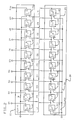
- Fig. 2 is a block diagram showing the elements of the ring counter 20 and the latch circuit 22 of the deserializer 10 of Fig. 1.
- the ring counter 20 has a plurality of stages or latches 31 through 40, one stage for each of the data bits Dl through D10, respectively.
- the ring counter 20 includes a CLOCK line 30 for providing the CLOCK signal to the C inputs of the latches 31 through 40.
- the odd numbered latches that is latches 31, 33, 35, 37 and 39 (herein designated L1 latches), latch on the positive going edge of the CLOCK signal, and the even numbered latches, that is 32, 34, 36, 38 and 40 (herein designated L2 latches), latch on the negative going edge of the CLOCK signal.
- each latch 31 through 40 is connected to the D input of the immediately following latch.
- the Q output of the L1 latch 31 is connected to the D input of the L2 latch 32.
- its Q output is connected to the D input of the L1 latch 31 via a conductor 29.
- the Q output of each of the latches 31 through 40 provides its respective output signal designated C1 through C10.
- the latch circuit 22 includes a plurality of L1 latches 41 through 50, one L1 latch for each of the latches 31 through 40 of the ring counter 20, respectively.
- the SDATA signal is connected to the D input of each of the latches 41 through 50 via a conductor 51.
- the C input of each of the latches 41 through 50 receives its respective clocking signal (one of the C1 through C10 signals) from its respective one of the latches 31 through 40 of the ring counter 20.
- the Q output of each of the latches 41 through 50 is connected to its respective data output terminal Dl through D10 for transmission of the data bits to their respective input terminals of the drivers 23 and 24 (see Fig. 1).
- the latches 31 through 39 of the ring counter 20 are initially reset such that their Q outputs are in the zero or low condition, and the latch 40 is set such that its Q output is in the one or high condition.
- the output signal C1 of latch 31 goes high. This high is input into the D input of the latch 32.
- the latch 32 latches the high on its input such that its output signal C2 goes high. Since the output signal C9 of latch 39 is low, the output signal C10, of the latch 40 also goes low on the first negative edge of the CLOCK signal on conductor 30.
- This low output signal C10 is inputted into the D input of the latch 31 via conductor 29 such that on the next positive going edge of the CLOCK signal on conductor 30, the output signal C1 of latch 31 also goes low.
- a counter signal (the initial high on the Q output of latch 40) is shifted throughout the length of the ring counter 20, appearing on each Q output of latches 31 through 40 as output signals C1 through C10, respectively.
- each signal C1 through C10 goes to its one or high condition, its connected positive edge triggered latch 41 through 50 of the latch circuit 22 is enabled.
- the data bit of the SDATA signal then on conductor 51 will be latched by the respective latch 41 through 50.
- each data bit latched into one of the latches 41 through 50 represents a data bit of the SERIAL-DATA signal received at the input 12 of Fig. 1.
- Fig. 3 is a block diagram of an alternate circuit for inputting the initial one or high condition into the D input of the L1 latch 31 of the ring counter 20.
- a multiple input NOR gate 55 has its inputs connected to the Q outputs of latches 32, 34, 36 and 38 to receive the C1, C4, C6 and C8 signals.
- the Q output of the NOR gate 55 is connected to the D input of the latch 31 of the ring counter 20. It will be understood that when the signals C1, C4, C6 and C8 are simultaneously in their zero conditions, a one or high will be placed on the D input of the latch 31 to restart the ring counter 20. It will thus be seen that the Q outputs of all of the even numbered latches, except for the last even numbered latch 40, are connected to the inputs of the NOR gate 55.
- the circuit of Fig. 3 has the advantage that it is self-correcting.
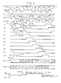
- Fig. 4 is a timing diagram showing the relationship of the SERIAL-DATA, PLL, SDATA, CLOCK, and C1 through C10 signals.
- Waveform 60 of Fig. 4 is an example of the SERIAL-DATA signal data bits which are inputted at input 12 of the deserializer 10 of Fig. 1.
- the SERIAL-DATA signal 60 has a series of serial bits 61 through 70 (which represent serial data bits 1-10 ⁇ .
- a one bit is being transmitted
- the signal 60 is at a low, such as at 62,66,68 and 70, a zero bit is being transmitted.
- FIG. 4 is an illustration of the PLL signal inputted into input 14 of the deserializer 10 of Fig. 1.
- the PLL signal 71 has positive going edges centered on each of the serial bits 61 through 70 of the SERIAL-DATA signal 60 which are used to sense the condition of the serial bits 61 through 70.
- the timing between the SERIAL-DATA signal 60 and the PLL signal 71 is preferred as it provides for sensing the values of the bits 61 through 70 when they are generally at a steady-state condition unaffected by skewing and propagation distortion caused by the transmission of the SERIAL-DATA signal over transmission lines.
- the waveform 72 of Fig. 4 is a waveform of the SDATA signal outputted at the Q output of the flip-flop 18 of Fig. 1.
- the flip-flop 18 is clocked by each positive going edge of the PLL signal, placing the bit value of the SERIAL-DATA signal then on the D input of flip-flop 18 on its Q output.
- the serial bits 61 through 70 are controlled or retimed by the flip-flop 18 to start at the positive going edge of the PLL signal of 71, as indicated by the bit values 61′ through 70′ of the SDATA signal 72.
- each transition of the CLOCK signal 74 will be generally centered on one of the data bits 61′ to 70′ of the retimed data signal SDATA 72.
- the C10 signal of the L2 latch 40 will go low at 90, which low is transmitted over conductor 29 to the D input of the Ll latch 31.
- the positive going edge 88 of the C2 signal inputted into the NOR gate 55 causes the output of NOR gate 55 to go low, which low is inputted into the D input of the L1 latch 31.
- the low condition inputted into the L1 latch 31 causes the C1 signal to have a negative going edge at 94 at the next positive going edge 96 of the CLOCK signal 74, thereby latching into the latch 41, the serial bit 61′ of the SDATA signal 72 which is then present on the conductor 51 of Fig. 2.
- the ring counter 20 of Figs. 1 and 2 will continue, in this fashion, to count in a sequential manner, latching the retimed data bits 62′ through 70′ into latches 42 through 50 in a similar manner.
- Waveform 105 of Fig. 4 shows when the bits 1-5 are valid
- waveform 106 shows when the bits 6-10 of the previous deserializer cycle are valid
- the relationship of the 105 and 106 waveform to the RBC signal 107 of the flip-flop 26 It will be seen that the RBC signal 107 has a positive going edge 108 generally in the center of the time when the bits 6-10 are valid, and a negative going edge 109 generally in the center of the time when the bits 1-5 are valid.
- edges 108 and 109 may be used as timing events to indicate when to start reading valid bits from the deserializer 10.
- the deserializer 10 does not provide for determining byte boundaries in the bits being deserialized. It is up to the user to properly establish a byte boundary.
- a skip bit function may be added to invert or non-invert the CLOCK signal to the ring counter 10, hence bumping the counter 20 by one bit. Such a skip bit function may then be used, in conjunction with byte boundary logic, to move the byte boundary one bit at a time, until byte synchronization is properly established.
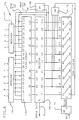
- Fig. 5 is a schematic diagram of one embodiment of two stages of the deserializer 10 of Figs. 1 and 2.
- the embodiment of Fig. 5 shows L1 latches 41 and 42 of the latch circuit 22, and the L1 latch 31 and L2 latch 32 of the ring counter 20.
- complementary logic is used.
- each input and output signal has a complement signal, such that inverters are not necessary. It is only necessary to exchange an input or output signal with its complement signal to effect an inversion. It will be understood that when using this logic, the inputs and outputs of the elements of Figs. 1, 2 and 3 will provide for both true signals and complemented signals.
- the CLOCK signal is inputted into the L1 latch 31 of the ring counter over a CLOCK signal conductor 110.
- the complement CLOCK signal designated CLOCK*, is inputted over a CLOCK* conductor 112.
- the base of a transistor 114 is connected to the CLOCK conductor 110, and the base of a transistor 116 is connected to the CLOCK* conductor 112.
- the emitters of the transistors 114 and 116 are connected to a current source shown as a grounded resistor 118.
- transistors 120 and 121 When the transistor 114 is turned on, a circuit is completed to transistors 120 and 121, whose bases, when the embodiment of Fig. 2 is used, receive the C10 signal and its complement C10*, respectively, from the tenth stage of the ring counter 20. When the embodiment of Fig. 3 is used, the bases of the transistors 120 and 121 will be connected to the outputs of the NOR gate 55.
- transistor 120 will be turned on, grounding the node 131 through transistors 120 and 114, whereas the complement signal C10* will be low holding off transistor 121 and allowing node 130 to rise to the voltage level of the voltage at 125 through resistor 127.
- the CLOCK* signal on conductor 112 goes high, transistor 116 will be turned on, latching the conditions of the nodes 130 and 131 by the action of cross-connected transistors 122 and 123.
- the base of a transistor 132 (the C terminal of the latch 41) is connected to the node 130, and the base of a transistor 133 (the C* terminal of the latch 41) is connected to the node 131.
- the emitters of the transistors 132 and 133 are connected to a current source shown as a grounded resistor 134.
- the turning on of transistor 132 completes a circuit to transistors 135 and 136 whose collectors are connected to a 5 volt voltage supply at 137 through resistors 139 and 140, respectively.
- the transistor 133 is turned on, a circuit is completed through transistors 141 and 142 whose collectors and bases are cross-coupled.
- the collectors of transistors 135 and 141 are connected at a node 143 (the Q* terminal of the latch 41), and the collectors of the transistors 136 and 142 are connected at a node 144 (the Q terminal of the latch 41).
- the Dl output of the latch circuit 22 (see Figs. 1 and 2) is connected to the Q node 144.
- the SDATA signal is supplied to a SDATA conductor 145, and the complement of the SDATA signal, designated SDATA*, is applied to a SDATA* conductor 146.
- the conductor 145 is connected to the base of the transistor 135 (the D terminal of the latch 41) and the conductor 136 is connected to the base of transistor 136 (The D* terminal of the latch 41).
- the transistor 132 when the C1 signal on the node 130 is high, and its complement C1*, on the node 131 is low, the transistor 132 will be turned on such that the condition on the SDATA conductor 145 appears on the Q output at node 144 and the connected D1 output. For instance, when the transistor 132 is turned on and the SDATA conductor 145 is high, transistor 135 will be turned on, grounding the Q* output at node 143 through the transistors 132 and 135. The complement signal SDATA* will be low, turning off transistor 136 such that the Q output at node 144 and the Dl output may rise to the value of the voltage at the terminal 137 through the resistor 139. As discussed in connection with Fig.
- the C1 signal on the base of the transistor 132 will remain high until the positive going edge 96 of the CLOCK signal.
- the C1 signal will then go low at 94, at which time its complement C1* will go high, turning on transistor 133 and latching the condition of the nodes 143 and 144 by the action of the cross-coupled transistors 141 and 142.
- the second stage of the deserializer circuit 10 is formed of transistors which are connected similar to those discussed in connection with latches 31 and 41, except that the L2 latch 32 is connected to trigger on negative going edges of the CLOCK signal. This is done by providing a transistor 150 which is similar to the transistor 114 except that its base is connected to the CLOCK* conductor 112, and a transistor 151 which is similar to the transistor 116 except that its base is connected to the CLOCK conductor 110. It will thus be understood that the L2 latch 32 latches the C1 signal and its complement C1* when the signal on the CLOCK* conductor 112 is high (when the CLOCK signal is low).
- the C1 and C2 signals from the ring counter 20 are each two CLOCK signal pulses wide, but which overlap for one CLOCK signal pulse width (see Fig. 4). Also, the latches 41 and 42 of the deserializer circuit 10 do not latch until the generally steady state condition of their respective bits (bits 61′ and 62′ of Fig. 4) are present on the SDATA conductor.
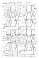
- Fig. 6 is a block diagram of another embodiment of the present invention connected as a serializer 170.
- the serializer 170 includes a divide-by-two circuit 171, ring counter 172 and NOR gate 173 which are similar to the divide-by-two circuit 16 of Fig. 1, the ring counter 20 of Figs. 1 and 2, and the NOR gate 55 of Fig. 3.
- An oscillator signal OSC which times the bit times of the serial data signal coming from the serializer 170, is inputted into the divide-by-two circuit 171, whose output supplies a clock signal DIV2 to the ring counter 172.
- the ring counter 172 has ten stages, each stage generating one of the output signals C1 through C10, respectively, as discussed in connection with the ring counter 20 of Figs. 1 and 2.
- the serializer 170 receives ten parallel bits, designated A through J, and places them on a SERIAL DATA line 175 as serial bits.
- the bits A through J are received from a parallel bus (not shown) in two bytes, the first byte having six bits and the second byte having four bits. Bits A, B, C, D, E and I of the first byte are simultaneously received by a first receiver 176, and bits F, G, H and J are simultaneously received by a second receiver 177.
- Each of the outputs of the receivers 176 and 177 is connected to one of the inputs of a latch circuit 178 having a plurality of latches such that each of the bits A through J received by the receivers 176 and 177 is latched into a respective latch of the latch circuit 178.
- a first read line 180 receives the C9 signal for controlling the simultaneous clocking of each of the bits A, B, C, D, E and I of the first byte into one of the first six latches of the latch circuit 178
- a second read line 181 receives the C5 signal for controlling the simultaneous clocking each of the bits F, G, H and J into one of the last four latches of the latches circuit 178.
- the signal C5 is inputted into the S terminal of a set-reset flip-flop 182, and the signal C9 is inputted into its R terminal.
- the Q output of the flip-flop 182 provides a transmission byte clock (TBC) signal for controlling the transmission of the data bytes to the receivers 176 and 177.
- TBC transmission byte clock
- the TBC signal instructs a bus controller (not shown) when to transmit bits of the respective bytes for receipt by the receivers 176 and 177.
- a selector circuit 185 is connected between the ring counter 172 and the latch circuit 178.
- the Q outputs of the stages of the ring counter 172 are connected to respective ones of the C inputs of the selector circuit 185, and the Q outputs of the latches of the latches circuit 178 are connected to respective ones of the corresponding D inputs of the selector circuit 185.
- the bit on the respective D input of the selector circuit 185 will be placed on its Q output for transmission to the connected SERIAL DATA line 175.
- the ring counter 172 sequentially enables the signals C1 through C10, which in turn addresses the respective C1 through C10 inputs of the selector 185 to cause the sequential transmission of the respective bits A through J from the latches circuit 178 to the SERIAL DATA line 175.
- Fig. 7 is a timing diagram of the various signals of the serializer circuit 170 of Fig. 6. It will be understood that the number of bits per byte, and the total number of bits serialized by the serializer circuit 170, may be changed as desired.
- latches 31 and 32 may be used for the stages of the counter 172 of the embodiment of Fig. 6.
- the construction of latches 41 and 42 may be used to construct the latches of the latch circuit 178.
- the CLOCK conductor 110 and its complement would carry the output DIV2 signal and its complement from the divide-by-two circuit 171.
- each D and D* input of each latch (for instance, the bases of transistors 135 and 136, respectively) would be connected to one of the outputs of the receivers 176 and 177.
- Each of the Q outputs (for instance, node 144 of the latch 41) would be connected to a separate Q input of a selector circuit 185, as discussed in connection with Fig. 6.
- the C and C* inputs of each latch (for instance, the bases of the transistors 132 and 133, respectively) would be connected to one of their respective read lines 180 or 181 (see Fig. 170) such that the latches would be controlled to simultaneously latch the parallel data bits as previously discussed.
Landscapes
- Engineering & Computer Science (AREA)
- Theoretical Computer Science (AREA)
- Logic Circuits (AREA)
- Dc Digital Transmission (AREA)
- Synchronisation In Digital Transmission Systems (AREA)
Applications Claiming Priority (2)
| Application Number | Priority Date | Filing Date | Title |
|---|---|---|---|
| US07/114,178 US4901076A (en) | 1987-10-29 | 1987-10-29 | Circuit for converting between serial and parallel data streams by high speed addressing |
| US114178 | 1987-10-29 |
Publications (2)
| Publication Number | Publication Date |
|---|---|
| EP0313875A2 true EP0313875A2 (fr) | 1989-05-03 |
| EP0313875A3 EP0313875A3 (fr) | 1990-11-14 |
Family
ID=22353770
Family Applications (1)
| Application Number | Title | Priority Date | Filing Date |
|---|---|---|---|
| EP19880116356 Ceased EP0313875A3 (fr) | 1987-10-29 | 1988-10-03 | Circuit convertisseur parallèle/série et série/parallèle |
Country Status (3)
| Country | Link |
|---|---|
| US (1) | US4901076A (fr) |
| EP (1) | EP0313875A3 (fr) |
| JP (1) | JPH01129616A (fr) |
Cited By (9)
| Publication number | Priority date | Publication date | Assignee | Title |
|---|---|---|---|---|
| US5003308A (en) * | 1989-03-29 | 1991-03-26 | International Business Machines Corporation | Serial data receiver with phase shift detection |
| EP0466592A1 (fr) * | 1990-07-11 | 1992-01-15 | Bull S.A. | Dispositif de sérialisation et de désérialisation de données et système de transmission numérique de données en série en résultant |
| US5260608A (en) * | 1990-02-06 | 1993-11-09 | Bull, S.A. | Phase-locked loop and resulting frequency multiplier |
| EP0645696A1 (fr) * | 1993-09-29 | 1995-03-29 | Kabushiki Kaisha Toshiba | Dispositif de mémoire à semi-conducteur, utilisant un pointeur sériel |
| US5430773A (en) * | 1990-07-11 | 1995-07-04 | Bull, S.A. | Data sampling apparatus, and resultant digital data transmission system |
| EP0856948A1 (fr) * | 1997-01-31 | 1998-08-05 | Oki Electric Industry Co., Ltd. | Convertisseur série-parallèle |
| RU2187887C2 (ru) * | 2000-10-30 | 2002-08-20 | Государственное унитарное предприятие Научно-производственное предприятие "Полет" | Преобразователь параллельного кода в последовательный |
| EP1202163A3 (fr) * | 2000-10-25 | 2004-09-08 | Seiko Epson Corporation | Convertisseur série-parallèle, dispositif de commande de transfert de données, et appareil électronique |
| WO2024035989A1 (fr) * | 2022-08-12 | 2024-02-15 | Qualcomm Incorporated | Communication inter-puces à faible puissance utilisant des lignes à retard |
Families Citing this family (33)
| Publication number | Priority date | Publication date | Assignee | Title |
|---|---|---|---|---|
| DE3789433T2 (de) * | 1986-12-27 | 1994-06-30 | Sony Corp | Gerät zur digitalen Kodeumwandlung. |
| JP2501513Y2 (ja) * | 1989-04-27 | 1996-06-19 | 日本電気株式会社 | 並列直列変換器 |
| EP0424554A1 (fr) * | 1989-10-23 | 1991-05-02 | Siemens Aktiengesellschaft | Convertisseur série-parallèle et/ou parallèle-série à plusieurs étages |
| FR2657739B1 (fr) * | 1990-01-26 | 1992-05-07 | Sgc Thomson Microelectronics Sa | Serialiseur/deserialiseur. |
| US5101203A (en) * | 1990-06-29 | 1992-03-31 | International Business Machines Corporation | Digital data regeneration and deserialization circuits |
| US5107264A (en) * | 1990-09-26 | 1992-04-21 | International Business Machines Corporation | Digital frequency multiplication and data serialization circuits |
| US5576980A (en) * | 1991-06-28 | 1996-11-19 | Texas Instruments Incorporated | Serializer circuit for loading and shifting out digitized analog signals |
| US5321400A (en) * | 1992-03-13 | 1994-06-14 | Nec Corporation | Serial data interface circuit dealing with a plurality of receiving modes |
| US6771249B1 (en) | 1995-01-13 | 2004-08-03 | Micron Technology, Inc. | Producing walking one pattern in shift register |
| US5598156A (en) * | 1995-01-13 | 1997-01-28 | Micron Display Technology, Inc. | Serial to parallel conversion with phase locked loop |
| US5638085A (en) * | 1995-01-13 | 1997-06-10 | Micron Display Technology, Inc. | Timing control for a matrixed scanned array |
| US5633899A (en) * | 1996-02-02 | 1997-05-27 | Lsi Logic Corporation | Phase locked loop for high speed data capture of a serial data stream |
| US5724361A (en) * | 1996-03-12 | 1998-03-03 | Lsi Logic Corporation | High performance n:1 multiplexer with overlap control of multi-phase clocks |
| US5805089A (en) * | 1996-09-05 | 1998-09-08 | Lsi Logic Corporation | Time-division data multiplexer with feedback for clock cross-over adjustment |
| US6018260A (en) * | 1997-08-06 | 2000-01-25 | Lucent Technologies Inc. | High-speed clock-enabled latch circuit |
| US5982309A (en) * | 1998-01-09 | 1999-11-09 | Iowa State University Research Foundation, Inc. | Parallel-to-serial CMOS data converter with a selectable bit width mode D flip-flop M matrix |
| US6020770A (en) * | 1998-05-06 | 2000-02-01 | Motorola, Inc. | Transparent latch-based sequencer and sequence controlling method |
| US6125406A (en) * | 1998-05-15 | 2000-09-26 | Xerox Corporation | Bi-directional packing data device enabling forward/reverse bit sequences with two output latches |
| US6065066A (en) * | 1998-06-02 | 2000-05-16 | Adaptec, Inc. | System for data stream packer and unpacker integrated circuit which align data stored in a two level latch |
| US6587942B1 (en) * | 2000-01-03 | 2003-07-01 | Oak Technology, Inc. | Circuit for converting input serial data in a plurality of possible formats into output data in parallel format by interpreting input data format indication information |
| DE10101718C1 (de) * | 2001-01-15 | 2002-06-06 | Infineon Technologies Ag | Datenempfangsschaltung |
| US6593863B2 (en) * | 2001-12-05 | 2003-07-15 | Parama Networks, Inc. | Serializer |
| JP4034172B2 (ja) * | 2002-11-20 | 2008-01-16 | Necエレクトロニクス株式会社 | エンコーダ、デコーダおよびデータ転送装置 |
| US7249273B2 (en) * | 2003-06-23 | 2007-07-24 | Intel Corporation | Synchronized serial interface |
| US7313660B2 (en) * | 2003-09-04 | 2007-12-25 | Lsi Corporation | Data stream frequency reduction and/or phase shift |
| US7336547B2 (en) * | 2004-02-27 | 2008-02-26 | Micron Technology, Inc. | Memory device having conditioning output data |
| US7925820B2 (en) * | 2004-09-30 | 2011-04-12 | Samsung Electronics Co., Ltd. | Nonvolatile semiconductor memory device and program method therefor |
| US7733248B2 (en) * | 2008-09-18 | 2010-06-08 | Fairchild Semiconductor Corporation | Measuring and regenerating a variable pulse width |
| US8970197B2 (en) * | 2012-08-03 | 2015-03-03 | United Microelectronics Corporation | Voltage regulating circuit configured to have output voltage thereof modulated digitally |
| US9154159B2 (en) * | 2013-12-31 | 2015-10-06 | International Business Machines Corporation | Low latency data deserializer |
| CN112562559B (zh) * | 2019-09-26 | 2023-05-30 | 京东方科技集团股份有限公司 | 计数器、像素电路、显示面板和显示设备 |
| CN112820225B (zh) * | 2019-11-15 | 2023-01-24 | 京东方科技集团股份有限公司 | 一种数据缓存电路、显示面板及显示装置 |
| CN112820226B (zh) * | 2019-11-15 | 2023-02-03 | 京东方科技集团股份有限公司 | 一种串并转换电路及显示面板 |
Family Cites Families (16)
| Publication number | Priority date | Publication date | Assignee | Title |
|---|---|---|---|---|
| US3017620A (en) * | 1957-03-08 | 1962-01-16 | Ibm | Ring checking circuit |
| US3792362A (en) * | 1972-10-30 | 1974-02-12 | Amdahl Corp | Clock apparatus and data processing system |
| JPS516841U (fr) * | 1974-06-28 | 1976-01-19 | ||
| US4015252A (en) * | 1975-06-25 | 1977-03-29 | The United States Of America As Represented By The Secretary Of The Navy | High speed serial data synchronization scheme |
| JPS5271949A (en) * | 1975-12-12 | 1977-06-15 | Hitachi Ltd | Desirializer |
| JPS5275140A (en) * | 1975-12-19 | 1977-06-23 | Hitachi Ltd | Series-parallel conversion circuit |
| NL7707540A (nl) * | 1977-07-07 | 1979-01-09 | Philips Nv | Inrichting voor het koderen van signalen die over een aantal kanalen worden verdeeld. |
| JPS55141823A (en) * | 1979-04-24 | 1980-11-06 | Fujitsu Ltd | Data read-out circuit |
| JPS56145426A (en) * | 1980-04-11 | 1981-11-12 | Sanyo Electric Co Ltd | Serial data transferring method |
| US4377806A (en) * | 1981-05-13 | 1983-03-22 | International Business Machines Corporation | Parallel to serial converter |
| US4642629A (en) * | 1983-04-18 | 1987-02-10 | Megabit Communications, Inc. | Enhanced distance data transmission system |
| DE3373730D1 (en) * | 1983-12-15 | 1987-10-22 | Ibm | Series-parallel/parallel-series device for variable bit length configuration |
| JPS60169947U (ja) * | 1984-04-17 | 1985-11-11 | 日本電気株式会社 | パラレル/シリアル変換回路 |
| US4620180A (en) * | 1985-10-21 | 1986-10-28 | Northern Telecom Limited | Serial-to-parallel converter for high-speed bit streams |
| US4692641A (en) * | 1986-02-13 | 1987-09-08 | Burr-Brown Corporation | Level shifting circuitry for serial-to-parallel converter |
| US4675652A (en) * | 1986-04-11 | 1987-06-23 | Quantum Corporation | Integrated encoder decoder for variable length, zero run length limited codes |
-
1987
- 1987-10-29 US US07/114,178 patent/US4901076A/en not_active Expired - Fee Related
-
1988
- 1988-08-18 JP JP63203980A patent/JPH01129616A/ja active Granted
- 1988-10-03 EP EP19880116356 patent/EP0313875A3/fr not_active Ceased
Cited By (14)
| Publication number | Priority date | Publication date | Assignee | Title |
|---|---|---|---|---|
| US5003308A (en) * | 1989-03-29 | 1991-03-26 | International Business Machines Corporation | Serial data receiver with phase shift detection |
| US5260608A (en) * | 1990-02-06 | 1993-11-09 | Bull, S.A. | Phase-locked loop and resulting frequency multiplier |
| US5430773A (en) * | 1990-07-11 | 1995-07-04 | Bull, S.A. | Data sampling apparatus, and resultant digital data transmission system |
| FR2664765A1 (fr) * | 1990-07-11 | 1992-01-17 | Bull Sa | Dispositif de serialisation et de deserialisation de donnees et systeme de transmission numerique de donnees en serie en resultant. |
| US5414830A (en) * | 1990-07-11 | 1995-05-09 | Bull, S.A. | Apparatus for serialization and deserialization of data, and resultant system for digital transmission of serial data |
| EP0466592A1 (fr) * | 1990-07-11 | 1992-01-15 | Bull S.A. | Dispositif de sérialisation et de désérialisation de données et système de transmission numérique de données en série en résultant |
| EP0645696A1 (fr) * | 1993-09-29 | 1995-03-29 | Kabushiki Kaisha Toshiba | Dispositif de mémoire à semi-conducteur, utilisant un pointeur sériel |
| US5469400A (en) * | 1993-09-29 | 1995-11-21 | Kabushiki Kaisha Toshiba | Semiconductor memory device using serial pointer |
| US5561633A (en) * | 1993-09-29 | 1996-10-01 | Kabushiki Kaisha Toshiba | Semiconductor memory device using serial pointer |
| EP0856948A1 (fr) * | 1997-01-31 | 1998-08-05 | Oki Electric Industry Co., Ltd. | Convertisseur série-parallèle |
| EP1202163A3 (fr) * | 2000-10-25 | 2004-09-08 | Seiko Epson Corporation | Convertisseur série-parallèle, dispositif de commande de transfert de données, et appareil électronique |
| RU2187887C2 (ru) * | 2000-10-30 | 2002-08-20 | Государственное унитарное предприятие Научно-производственное предприятие "Полет" | Преобразователь параллельного кода в последовательный |
| WO2024035989A1 (fr) * | 2022-08-12 | 2024-02-15 | Qualcomm Incorporated | Communication inter-puces à faible puissance utilisant des lignes à retard |
| US12267075B2 (en) | 2022-08-12 | 2025-04-01 | Qualcomm Incorporated | Low-power inter-die communication using delay lines |
Also Published As
| Publication number | Publication date |
|---|---|
| US4901076A (en) | 1990-02-13 |
| JPH0442853B2 (fr) | 1992-07-14 |
| EP0313875A3 (fr) | 1990-11-14 |
| JPH01129616A (ja) | 1989-05-22 |
Similar Documents
| Publication | Publication Date | Title |
|---|---|---|
| US4901076A (en) | Circuit for converting between serial and parallel data streams by high speed addressing | |
| US5361290A (en) | Clock generating circuit for use in single chip microcomputer | |
| US6339387B1 (en) | Serial/parallel converter | |
| JP2000236260A (ja) | 信号符号化回路及び信号符号化方法 | |
| JPH0678019A (ja) | インターフェース装置 | |
| US4703495A (en) | High speed frequency divide-by-5 circuit | |
| US4079372A (en) | Serial to parallel converter | |
| GB2044045A (en) | Data transmission system | |
| JPS62188446A (ja) | 同期検出回路及び方法 | |
| US4118791A (en) | Multi-level encoding system | |
| US4315166A (en) | Frequency divider arrangement | |
| JP2639410B2 (ja) | ロード可能なリプルカウンタ | |
| US20040004564A1 (en) | Parallel /serial conversion circuit, serial data generation circuit, synchronization signal generation circuit, clock signal generation circuit, serial data transmission device, serial data reception device, and serial data transmission system | |
| US3984702A (en) | N-bit register system using CML circuits | |
| EP0064590B1 (fr) | Compteur binaire à grande vitesse | |
| US4539680A (en) | Chip to chip information bit transmission process and device | |
| JP2831788B2 (ja) | フリップフロップ回路 | |
| US6215728B1 (en) | Data storage device capable of storing plural bits of data | |
| US6271701B1 (en) | Resetting flip-flop structures and methods for high-rate trigger generation and event monitoring | |
| JPH11509658A (ja) | 拡張されたチップ選択リセット装置および方法 | |
| US3350579A (en) | n-state control circuit | |
| KR0158902B1 (ko) | 마스터/슬레이브 보드간의 직렬데이타 송수신 장치 및 방법 | |
| US4201927A (en) | Circuit for producing sequentially spaced pulses | |
| US4669101A (en) | High speed counter with decoding means and means for selecting second and higher order counter stages to be toggled | |
| JPH0748664B2 (ja) | 直並列変換器 |
Legal Events
| Date | Code | Title | Description |
|---|---|---|---|
| PUAI | Public reference made under article 153(3) epc to a published international application that has entered the european phase |
Free format text: ORIGINAL CODE: 0009012 |
|
| AK | Designated contracting states |
Kind code of ref document: A2 Designated state(s): DE FR GB |
|
| 17P | Request for examination filed |
Effective date: 19890809 |
|
| PUAL | Search report despatched |
Free format text: ORIGINAL CODE: 0009013 |
|
| AK | Designated contracting states |
Kind code of ref document: A3 Designated state(s): DE FR GB |
|
| 17Q | First examination report despatched |
Effective date: 19930803 |
|
| STAA | Information on the status of an ep patent application or granted ep patent |
Free format text: STATUS: THE APPLICATION HAS BEEN REFUSED |
|
| 18R | Application refused |
Effective date: 19941030 |