EP0314299A2 - Méthode et appareil de traitement de gaz d'échappement provenant de procédé de fabrication de semi-conducteur - Google Patents
Méthode et appareil de traitement de gaz d'échappement provenant de procédé de fabrication de semi-conducteur Download PDFInfo
- Publication number
- EP0314299A2 EP0314299A2 EP88308879A EP88308879A EP0314299A2 EP 0314299 A2 EP0314299 A2 EP 0314299A2 EP 88308879 A EP88308879 A EP 88308879A EP 88308879 A EP88308879 A EP 88308879A EP 0314299 A2 EP0314299 A2 EP 0314299A2
- Authority
- EP
- European Patent Office
- Prior art keywords
- absorbent
- bypass valve
- waste gas
- gas
- reaction chamber
- Prior art date
- Legal status (The legal status is an assumption and is not a legal conclusion. Google has not performed a legal analysis and makes no representation as to the accuracy of the status listed.)
- Granted
Links
- 239000002912 waste gas Substances 0.000 title claims abstract description 36
- 238000000034 method Methods 0.000 title claims abstract description 22
- 239000004065 semiconductor Substances 0.000 title claims abstract description 21
- 238000004519 manufacturing process Methods 0.000 title claims abstract description 20
- 239000007789 gas Substances 0.000 claims abstract description 40
- 230000002745 absorbent Effects 0.000 claims abstract description 36
- 239000002250 absorbent Substances 0.000 claims abstract description 36
- 238000006243 chemical reaction Methods 0.000 claims abstract description 33
- 231100000252 nontoxic Toxicity 0.000 claims abstract description 15
- 230000003000 nontoxic effect Effects 0.000 claims abstract description 15
- 239000002341 toxic gas Substances 0.000 claims abstract description 13
- 239000007787 solid Substances 0.000 claims abstract description 11
- 238000010926 purge Methods 0.000 claims description 9
- 239000010891 toxic waste Substances 0.000 claims description 4
- 230000004044 response Effects 0.000 claims description 3
- 238000013022 venting Methods 0.000 claims description 2
- 238000007599 discharging Methods 0.000 claims 1
- 231100000331 toxic Toxicity 0.000 claims 1
- 230000002588 toxic effect Effects 0.000 claims 1
- 239000002245 particle Substances 0.000 abstract description 5
- 235000012431 wafers Nutrition 0.000 description 9
- 230000008569 process Effects 0.000 description 7
- 238000001035 drying Methods 0.000 description 4
- 238000005530 etching Methods 0.000 description 4
- 239000011261 inert gas Substances 0.000 description 4
- 230000000694 effects Effects 0.000 description 3
- 238000002347 injection Methods 0.000 description 2
- 239000007924 injection Substances 0.000 description 2
- 238000005268 plasma chemical vapour deposition Methods 0.000 description 2
- 238000001020 plasma etching Methods 0.000 description 2
- 238000010521 absorption reaction Methods 0.000 description 1
- 230000009471 action Effects 0.000 description 1
- 239000007795 chemical reaction product Substances 0.000 description 1
- 238000005260 corrosion Methods 0.000 description 1
- 230000007797 corrosion Effects 0.000 description 1
- 238000013461 design Methods 0.000 description 1
- 238000006073 displacement reaction Methods 0.000 description 1
- 238000007689 inspection Methods 0.000 description 1
- 238000012423 maintenance Methods 0.000 description 1
- 238000012986 modification Methods 0.000 description 1
- 230000004048 modification Effects 0.000 description 1
- 238000012856 packing Methods 0.000 description 1
- 230000008439 repair process Effects 0.000 description 1
- 230000000630 rising effect Effects 0.000 description 1
- 238000007789 sealing Methods 0.000 description 1
- 238000001179 sorption measurement Methods 0.000 description 1
Images
Classifications
-
- B—PERFORMING OPERATIONS; TRANSPORTING
- B01—PHYSICAL OR CHEMICAL PROCESSES OR APPARATUS IN GENERAL
- B01D—SEPARATION
- B01D53/00—Separation of gases or vapours; Recovering vapours of volatile solvents from gases; Chemical or biological purification of waste gases, e.g. engine exhaust gases, smoke, fumes, flue gases, aerosols
- B01D53/34—Chemical or biological purification of waste gases
-
- B—PERFORMING OPERATIONS; TRANSPORTING
- B01—PHYSICAL OR CHEMICAL PROCESSES OR APPARATUS IN GENERAL
- B01D—SEPARATION
- B01D53/00—Separation of gases or vapours; Recovering vapours of volatile solvents from gases; Chemical or biological purification of waste gases, e.g. engine exhaust gases, smoke, fumes, flue gases, aerosols
- B01D53/34—Chemical or biological purification of waste gases
- B01D53/46—Removing components of defined structure
Definitions
- the present invention relates to a method of and apparatus for treating waste gas from a semiconductor manufacturing process. More particularly, the present invention pertains to a method which is suitable for treating such a waste gas with a dry solid absorbent. The present invention is also concerned with an apparatus which may be effectively employed to practice this waste gas treatment method.
- the present invention provides a method of treating waste gas from semiconductor manufacturing equipment with a dry absorbent wherein a bypass pipe which is equipped with a bypass valve is provided between inlet and outlet pipes of a container packed with the absorbent and wherein a wafer is set in a reaction chamber of the semiconductor manufacturing equipment under atmospheric pressure, and then, when the reaction chamber is evacuated to a level below that of atmospheric pressure, the bypass valve is opened to prevent a large amount of the non-toxic gas that is discharged from the reaction chamber during the evacuation from being fed to the absorbent-packet container.
- the semiconductor manufacturing equipment 2 may be of any type, provided that the equipment treats wafers under a high vacuum in a process such as plasma CVD or plasma etching, and therefore the kind and flow rate of process gas 1 may also be selected as desired in accordance with the conditions of each individual process. Further, it is also possible to select as desired the kind and amount of absorbent which is to be packed in the container 10 and the dimensions and configuration of the packed container 10.
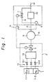
- the process gas 1 is fed into a reaction chamber 14 of the semiconductor manufacturing equipment 2 to react with wafers, and the waste gas generated after the reaction is sent by the operation of an evacuating device 5 to the absorbent-packed container 10 where it is made harmless before being discharged.
- a bypass valve 7 is opened to release a large amount of the non-toxic gas from the reaction chamber 14 through a bypass pipe 8, thereby preventing the large amount of flowing gas from being passed through the absorbent-packed container 10. Since the large amount of gas is not discharged until a main valve 3 is opened, the bypass valve 7 may be opened in advance on the basis of a signal for opening the main valve 3.
- the bypass valve 7 is also left open unless otherwise arranged. Therefore, the bypass valve 7 is arranged to be closed by the action of a timer after a predetermined period of time has elapsed. It is possible to set the timer to any period of time so long as it is one within which the flow rate of the discharged gas and the inlet pressure of the absorbent-packed container 10 can drop sufficiently and within which no process gas will be fed into the reaction chamber 14.
- the arrangement may be such that such a rise in pressure is detected by means of a pressure sensor 9 and the bypass valve 7 is opened in response to a signal output from the pressure sensor 9.
- a hunting phenomenon may occur in which, at the same time as the bypass valve 7 is opened, the inlet pressure lowers, and the pressure sensor 9, which detects this lowering in pressure, closes the bypass valve 7, resulting in the pressure rising such as to cause the bypass valve 7 to open again.
- waste gas stays in a waste gas pipe 4 which extends from the evacuating device 5 to the absorbent-packed container 10 immediately after the completion of wafer treatment, if, in this state, a large amount of the non-toxic gas is discharged via the bypass valve 7, part of the waste gas which is to be removed may be released in the form of an untreated waste gas. For this reason, it is preferivelyable to purge the waste gas remaining in the pipe 4 with an inert gas introduced through a pipe 6 so that the residual waste gas is fed to the absorbent-packed container 10 before the reaction chamber 14 is evacuated, and then to open the bypass valve 7 to release a large amount of the non-toxic gas in the reaction chamber.
- the inert purging gas may be injected into the evacuating device 5 or from an appropriate position which is immediately downstream of it, and the injection of the inert purging gas may be effected either at all times or for a predetermined period of time immediately before the evacuation of the reaction chamber 14.
- the flow rate of the injected inert gas should be determined by taking into consideration the volume of the pipe, the injection time and so forth. It should be noted that the treated waste gas is discharged through a waste gas pipe 12.
- the flow rate of gas which is fed to the absorbent-packed container is only about several liters per minute. Therefore, even when the particle diameter of the absorbent is reduced considerably to increase the surface area and thereby improve the reaction efficiency, the resistance to gas flow is maintained at a low level. Accordingly, the load on the device used to evacuate the reaction chamber is reduced, and the toxic waste gas treatment can be conducted safely.
- Fig. 1 the driving sequence is given and the feature of the present invention is explained.
Landscapes
- Engineering & Computer Science (AREA)
- Chemical & Material Sciences (AREA)
- Health & Medical Sciences (AREA)
- Biomedical Technology (AREA)
- Environmental & Geological Engineering (AREA)
- Analytical Chemistry (AREA)
- General Chemical & Material Sciences (AREA)
- Oil, Petroleum & Natural Gas (AREA)
- Chemical Kinetics & Catalysis (AREA)
- Treating Waste Gases (AREA)
- Drying Of Semiconductors (AREA)
Applications Claiming Priority (2)
| Application Number | Priority Date | Filing Date | Title |
|---|---|---|---|
| JP23885987 | 1987-09-25 | ||
| JP238859/87 | 1987-09-25 |
Publications (3)
| Publication Number | Publication Date |
|---|---|
| EP0314299A2 true EP0314299A2 (fr) | 1989-05-03 |
| EP0314299A3 EP0314299A3 (en) | 1990-05-16 |
| EP0314299B1 EP0314299B1 (fr) | 1993-06-09 |
Family
ID=17036320
Family Applications (1)
| Application Number | Title | Priority Date | Filing Date |
|---|---|---|---|
| EP88308879A Expired - Lifetime EP0314299B1 (fr) | 1987-09-25 | 1988-09-23 | Méthode et appareil de traitement de gaz d'échappement provenant de procédé de fabrication de semi-conducteur |
Country Status (4)
| Country | Link |
|---|---|
| US (1) | US4906257A (fr) |
| EP (1) | EP0314299B1 (fr) |
| KR (1) | KR960012559B1 (fr) |
| DE (1) | DE3881638T2 (fr) |
Cited By (1)
| Publication number | Priority date | Publication date | Assignee | Title |
|---|---|---|---|---|
| US9029244B2 (en) | 2005-01-19 | 2015-05-12 | Samsung Electronics Co., Ltd. | Apparatus including 4-way valve for fabricating semiconductor device, method of controlling valve, and method of fabricating semiconductor device using the apparatus |
Families Citing this family (12)
| Publication number | Priority date | Publication date | Assignee | Title |
|---|---|---|---|---|
| US5376163A (en) * | 1993-05-18 | 1994-12-27 | Andros Incorporated | Filter system |
| US5782942A (en) * | 1996-01-11 | 1998-07-21 | Vanguard International Semiconductor Corporation | Filter system for semiconductor furnace |
| US6149729A (en) * | 1997-05-22 | 2000-11-21 | Tokyo Electron Limited | Film forming apparatus and method |
| KR100242956B1 (ko) * | 1997-06-03 | 2000-02-01 | 윤종용 | 가스 배기 시스템의 잔류물 제거 및 차단장치 |
| US6106626A (en) * | 1998-12-03 | 2000-08-22 | Taiwan Semincondutor Manufacturing Company, Ltd | Apparatus and method for preventing chamber contamination |
| JP4092821B2 (ja) * | 1999-07-27 | 2008-05-28 | 東京エレクトロン株式会社 | 処理装置の排気システム |
| KR100320744B1 (ko) * | 1999-11-03 | 2002-01-19 | 김경균 | 폐가스 처리 시스템 |
| KR100361667B1 (ko) * | 2000-10-31 | 2002-11-22 | 유니셈 주식회사 | 폐가스 처리 장치 |
| US20040000515A1 (en) * | 2002-06-26 | 2004-01-01 | Harris James Jeffrey | Filter back-flushing reaction chamber apparatus |
| US6835233B2 (en) * | 2003-02-20 | 2004-12-28 | Taiwan Semiconductor Manufacturing Co., Ltd | Method and apparatus for reducing particle contamination |
| US7964017B2 (en) | 2006-05-05 | 2011-06-21 | General Dynamics Armament And Technical Products, Inc. | Systems and methods for controlling moisture level in a gas |
| US7963146B2 (en) * | 2007-05-14 | 2011-06-21 | General Dynamics Armament And Technical Products, Inc. | Method and system for detecting vapors |
Family Cites Families (5)
| Publication number | Priority date | Publication date | Assignee | Title |
|---|---|---|---|---|
| US1677804A (en) * | 1923-01-29 | 1928-07-17 | Ubald R Loranger | Gas scrubber for refrigerating apparatus |
| US3545500A (en) * | 1967-12-21 | 1970-12-08 | Sylvania Electric Prod | Vacuum system |
| CH469239A (de) * | 1968-08-05 | 1969-02-28 | Balzers Patent Beteilig Ag | Vakuumofenanlage |
| GB1239852A (en) * | 1969-01-09 | 1971-07-21 | Ferranti Ltd | Improvements relating to semiconductor devices |
| FR2069486A5 (fr) * | 1969-12-24 | 1971-09-03 | Draegerwerk Ag |
-
1988
- 1988-09-23 EP EP88308879A patent/EP0314299B1/fr not_active Expired - Lifetime
- 1988-09-23 DE DE8888308879T patent/DE3881638T2/de not_active Expired - Fee Related
- 1988-09-23 US US07/248,905 patent/US4906257A/en not_active Expired - Lifetime
- 1988-09-24 KR KR1019880012416A patent/KR960012559B1/ko not_active Expired - Fee Related
Cited By (3)
| Publication number | Priority date | Publication date | Assignee | Title |
|---|---|---|---|---|
| US9029244B2 (en) | 2005-01-19 | 2015-05-12 | Samsung Electronics Co., Ltd. | Apparatus including 4-way valve for fabricating semiconductor device, method of controlling valve, and method of fabricating semiconductor device using the apparatus |
| US9406502B2 (en) | 2005-01-19 | 2016-08-02 | Samsung Electronics Co., Ltd. | Apparatus including 4-way valve for fabricating semiconductor device, method of controlling valve, and method of fabricating semiconductor device using the apparatus |
| US9702041B2 (en) | 2005-01-19 | 2017-07-11 | Samsung Electronics Co., Ltd. | Apparatus including 4-way valve for fabricating semiconductor device, method of controlling valve, and method of fabricating semiconductor device using the apparatus |
Also Published As
| Publication number | Publication date |
|---|---|
| DE3881638D1 (de) | 1993-07-15 |
| KR960012559B1 (ko) | 1996-09-23 |
| KR890004764A (ko) | 1989-05-09 |
| EP0314299A3 (en) | 1990-05-16 |
| EP0314299B1 (fr) | 1993-06-09 |
| US4906257A (en) | 1990-03-06 |
| DE3881638T2 (de) | 1993-09-23 |
Similar Documents
| Publication | Publication Date | Title |
|---|---|---|
| US5114683A (en) | Thermal decomposition trap | |
| EP0314299B1 (fr) | Méthode et appareil de traitement de gaz d'échappement provenant de procédé de fabrication de semi-conducteur | |
| US5749159A (en) | Method for precision cleaning and drying surfaces | |
| KR100257305B1 (ko) | 열처리장치 및 그의 크리닝 방법 | |
| TWI388729B (zh) | 用於真空泵浦之前級預處理 | |
| CN1195419A (zh) | 核电厂内安全壳气氛惰性化与通风的设备和方法 | |
| JP2001044185A (ja) | 処理装置の排気システム | |
| WO2015080627A1 (fr) | Système de purification d'un milieu gazeux afin d'éliminer l'hydrogène et procédé d'exploitation | |
| US4479927A (en) | Regenerable cold trap for aluminum chloride effluent | |
| JP3545672B2 (ja) | 基板処理方法及び基板処理装置 | |
| KR20220046989A (ko) | 기판처리장치 | |
| US5635242A (en) | Method and apparatus for preventing rupture and contamination of an ultra-clean APCVD reactor during shutdown | |
| JPH113867A (ja) | 半導体製造装置 | |
| US5931663A (en) | Purge system for regenerative thermal oxidizer | |
| JPH0461686B2 (fr) | ||
| KR100266681B1 (ko) | 반도체 웨이퍼 제조용 식각장비의 세정장치 | |
| KR19980069172A (ko) | 가스 공급 시스템의 잔류 가스 배기 방법 | |
| JPH10125652A (ja) | 半導体製造装置 | |
| KR920004962B1 (ko) | 내화금속박막증착용 반도체장치의 진공배기계 | |
| JP4304354B2 (ja) | 半導体装置の処理方法 | |
| WO2025104916A1 (fr) | Dispositif de détoxication et procédé de détoxication pour gaz | |
| KR100790282B1 (ko) | 반도체 제조 장치의 배기 시스템 및 이에 적용된트랩부에서의 액상 티이오에스 배출 방법 | |
| JPH1194979A (ja) | 格納容器ベント設備 | |
| JPS60107247A (ja) | イオン打込装置のクライオポンプ再生装置 | |
| JP3442235B2 (ja) | 油拡散ポンプ及び半導体製造装置 |
Legal Events
| Date | Code | Title | Description |
|---|---|---|---|
| PUAI | Public reference made under article 153(3) epc to a published international application that has entered the european phase |
Free format text: ORIGINAL CODE: 0009012 |
|
| AK | Designated contracting states |
Kind code of ref document: A2 Designated state(s): DE FR GB |
|
| PUAL | Search report despatched |
Free format text: ORIGINAL CODE: 0009013 |
|
| AK | Designated contracting states |
Kind code of ref document: A3 Designated state(s): DE FR GB |
|
| 17P | Request for examination filed |
Effective date: 19901026 |
|
| 17Q | First examination report despatched |
Effective date: 19911210 |
|
| GRAA | (expected) grant |
Free format text: ORIGINAL CODE: 0009210 |
|
| AK | Designated contracting states |
Kind code of ref document: B1 Designated state(s): DE FR GB |
|
| REF | Corresponds to: |
Ref document number: 3881638 Country of ref document: DE Date of ref document: 19930715 |
|
| ET | Fr: translation filed | ||
| PLBE | No opposition filed within time limit |
Free format text: ORIGINAL CODE: 0009261 |
|
| STAA | Information on the status of an ep patent application or granted ep patent |
Free format text: STATUS: NO OPPOSITION FILED WITHIN TIME LIMIT |
|
| 26N | No opposition filed | ||
| PGFP | Annual fee paid to national office [announced via postgrant information from national office to epo] |
Ref country code: FR Payment date: 19980929 Year of fee payment: 11 |
|
| PGFP | Annual fee paid to national office [announced via postgrant information from national office to epo] |
Ref country code: DE Payment date: 19980930 Year of fee payment: 11 |
|
| PG25 | Lapsed in a contracting state [announced via postgrant information from national office to epo] |
Ref country code: FR Free format text: LAPSE BECAUSE OF NON-PAYMENT OF DUE FEES Effective date: 20000531 |
|
| PG25 | Lapsed in a contracting state [announced via postgrant information from national office to epo] |
Ref country code: DE Free format text: LAPSE BECAUSE OF NON-PAYMENT OF DUE FEES Effective date: 20000701 |
|
| REG | Reference to a national code |
Ref country code: FR Ref legal event code: ST |
|
| REG | Reference to a national code |
Ref country code: GB Ref legal event code: IF02 |
|
| PGFP | Annual fee paid to national office [announced via postgrant information from national office to epo] |
Ref country code: GB Payment date: 20030917 Year of fee payment: 16 |
|
| PG25 | Lapsed in a contracting state [announced via postgrant information from national office to epo] |
Ref country code: GB Free format text: LAPSE BECAUSE OF NON-PAYMENT OF DUE FEES Effective date: 20040923 |
|
| GBPC | Gb: european patent ceased through non-payment of renewal fee |
Effective date: 20040923 |