EP0314522B1 - Verfahren zum Ätzen von Gräben - Google Patents
Verfahren zum Ätzen von Gräben Download PDFInfo
- Publication number
- EP0314522B1 EP0314522B1 EP88310219A EP88310219A EP0314522B1 EP 0314522 B1 EP0314522 B1 EP 0314522B1 EP 88310219 A EP88310219 A EP 88310219A EP 88310219 A EP88310219 A EP 88310219A EP 0314522 B1 EP0314522 B1 EP 0314522B1
- Authority
- EP
- European Patent Office
- Prior art keywords
- etching
- trench
- substrate
- trench etching
- etching process
- Prior art date
- Legal status (The legal status is an assumption and is not a legal conclusion. Google has not performed a legal analysis and makes no representation as to the accuracy of the status listed.)
- Expired - Lifetime
Links
Images


Classifications
-
- H—ELECTRICITY
- H10—SEMICONDUCTOR DEVICES; ELECTRIC SOLID-STATE DEVICES NOT OTHERWISE PROVIDED FOR
- H10P—GENERIC PROCESSES OR APPARATUS FOR THE MANUFACTURE OR TREATMENT OF DEVICES COVERED BY CLASS H10
- H10P50/00—Etching of wafers, substrates or parts of devices
- H10P50/69—Etching of wafers, substrates or parts of devices using masks for semiconductor materials
- H10P50/691—Etching of wafers, substrates or parts of devices using masks for semiconductor materials for Group V materials or Group III-V materials
- H10P50/692—Etching of wafers, substrates or parts of devices using masks for semiconductor materials for Group V materials or Group III-V materials characterised by their composition, e.g. multilayer masks or materials
-
- H—ELECTRICITY
- H10—SEMICONDUCTOR DEVICES; ELECTRIC SOLID-STATE DEVICES NOT OTHERWISE PROVIDED FOR
- H10P—GENERIC PROCESSES OR APPARATUS FOR THE MANUFACTURE OR TREATMENT OF DEVICES COVERED BY CLASS H10
- H10P50/00—Etching of wafers, substrates or parts of devices
- H10P50/20—Dry etching; Plasma etching; Reactive-ion etching
- H10P50/24—Dry etching; Plasma etching; Reactive-ion etching of semiconductor materials
- H10P50/242—Dry etching; Plasma etching; Reactive-ion etching of semiconductor materials of Group IV materials
-
- H—ELECTRICITY
- H10—SEMICONDUCTOR DEVICES; ELECTRIC SOLID-STATE DEVICES NOT OTHERWISE PROVIDED FOR
- H10P—GENERIC PROCESSES OR APPARATUS FOR THE MANUFACTURE OR TREATMENT OF DEVICES COVERED BY CLASS H10
- H10P50/00—Etching of wafers, substrates or parts of devices
- H10P50/69—Etching of wafers, substrates or parts of devices using masks for semiconductor materials
- H10P50/691—Etching of wafers, substrates or parts of devices using masks for semiconductor materials for Group V materials or Group III-V materials
- H10P50/693—Etching of wafers, substrates or parts of devices using masks for semiconductor materials for Group V materials or Group III-V materials characterised by their size, orientation, disposition, behaviour or shape, in horizontal or vertical plane
- H10P50/694—Etching of wafers, substrates or parts of devices using masks for semiconductor materials for Group V materials or Group III-V materials characterised by their size, orientation, disposition, behaviour or shape, in horizontal or vertical plane characterised by their behaviour during the process, e.g. soluble masks or redeposited masks
Definitions
- the present invention relates to a trench etching process.
- the trench etching process for, for example, silicon has become extremely important when miniaturizing the area of the isolation and capacitor cells.
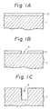
- FIG. 1A A prior-proposed trench etching process is shown in Figures 1A to 1C.
- a phosphosilicate glass (PSG) layer 2 having a thickness of, for example, 1.0 ⁇ m is formed on a silicon substrate 1, as shown in Fig. 1B, an opening 3 by which the silicon substrate 1 is exposed is formed in the PSG layer 2 in which a trench is to be formed, by photolithography.
- a trench 4 is formed in the silicon substrate 1 by a reactive ion etching (RIE) process using the remaining PSG layer 2 as a mask.
- RIE reactive ion etching
- the RIE process for producing a required trench is usually carried out by a time control, i. e. the time is predetermined by calculating the etching rate of the RIE of the silicon substrate.
- the RIE process for producing the required trench can also becarried out while monitoring the depth of the trench by calculating a difference between the time when laser beam is reflected from the surface of the silicon substrate and from the bottom surface of the trench.
- Such a trench etching process wherein a time control is carried out, is disadvantageous in that there is no guarantee that a required etching has been carried out, since no warning is given if a required etching is not realized due to unforeseen circumstances. Further, when the depth of trench is monitored by using a laser beam, etc., the monitoring precision is reduced due to the shape of the trench.
- Japanese Unexamined Patent Publication discloses a process for etching a semiconductor substrate wherein an etching end point is detected by monitoring the emission intensity of an atom or molecule or an ion of components of an etching mask.
- a completion of a trench etching can be precisely and reproducibly detected, but when many trenches having the same depth are formed in a silicon substrate, a uniform distribution of the depth of the trenches can not be obtained over an entire surface of the silicon substrate, since the etching mask is not directly laid on the silicon substrate and the etching rate of the film disposed between the etching mask and the silicon substrate is not the same as that of the silicon substrate.
- An embodiment of the present invention may provide a trench etching process wherein a completion of the trench etching can be precisely detected.
- An embodiment of the present invention may provide a trench etching process wherein a precise trench etching can be carried out reproducibly.
- An embodiment of the present invention may also provide a trench etching process wherein trenches having substantially the same depth can be obtained over an entire surface of, for example, a silicon substrate.
- a trench etching process comprising the steps of: preparing a substrate; forming a mask pattern for trench etching, comprising a material different from the material of the substrate, directly on the substrate; commencing etching of a plurality of trenches in the substrate using the mask; detecting the results of emission spectroanalyses generated by etching the mask pattern and the exposed portions of the substrate; and determining the completion of the trench etching using a predetermined change in the spectroanalysis results indicating that the said mask pattern has been removed from the entire surface of the substrate.
- a silicon or other semiconductor substrate is preferably used.
- the mask pattern is preferably made of phospho-silicate glass or thermal oxide of silicon.
- an etching mask of, for example, phosphosilicate glass (PSG) film 2 having a thickness of 1 ⁇ m is formed on a surface of a silicon substrate 1.
- PSG phosphosilicate glass
- a trench etching process is carried out under the following etching conditions, using a reactive ion etching device (RIE device).
- RIE device reactive ion etching device
- Reactive gas ⁇ carbon tetrachloride (CCl4) + chlorine gas (Cl2) Pressure in reaction chamber ?? 13 Pa (0.1 Torr)
- High frequency electrical power ⁇ 700 W
- 4 denotes a trench and 5 denotes ions of the reactive gas.
- the PSG film 2 may be completely removed at a portion, for example, region B, of the silicon substrate but still remains at, for example, region A, due to, for example, a deviation of the thickness of PSG film 2 on the surface of the silicon substrate, or the surface roughness, etc., as shown in Fig. 2C.
- the PSG film 2 is completely removed from all portions of the surface of the silicon substrate, including the regions A and B, as shown in Fig. 2D.
- the 603 nm spectral emission which is present until all of the PSG film 2 has been removed, disappears or decreases markedly.
- the 603 nm emission is markedly reduced, and thus, when changes in the results of emission spectroanalysis are generated, e.g. the spectral emission has vanished or markedly decreased, it is determined that the trench etching is completed.
- the time from the removal of the mask, i.e., the PSG film 2, at one portion to the time of the completion of the etching varies in different positions of the wafer surface, and the depth of trench formed by etching after the mask has been removed varies due to the difference in etching speeds for the trench per se and for the surrounding surface of the silicon substrate 1.
- the material of the inner portion of the trench and of the surrounding surface is the same, i.e. silicon, there is no difference in the etching speed thereof. Further, the period from the removal of the mask to the end of the trench etching is very short, compared with the total etching period.
- the depth L1 is substantially the same as the depth L2 , and thus the depth of a trench in region B becomes the same as that of a trench in region A, and thus, according to this embodiment, a control of a distribution of trenches having the same depth can be carried out.
- D1 D2
- ⁇ and ⁇ are in general both positive and of similar magnitude, ⁇ is larger than ( ⁇ - ⁇ )/(1+ ⁇ ), and consequently, T2/T1 is nearer to 1 than S2/S1, with the result that a more uniform trench etching depth can be obtained.
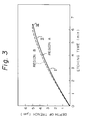
- Fig.3 illustrates a relationship between the etching time and the depth of trenches in region A and B of the silicon substrate.
- the steps I, II and III in Fig.3 correspond to Figs.2B, 2C, and 2D, and show the first stage, the middle stage, and the completion of the trench etching.
- the depths of trenches in the region B are slightly larger than those in region A, but on the other hand, upon completion of the etching, the depths of trenches in the region B are slightly less than that in region A.
- etching processes can be used with the process according to the invention, such as ECR (Electron Cyclotron Resonance) etching or MRIE (Magnetron Reactive Ion) etching.
- ECR Electro Cyclotron Resonance
- MRIE Magnetic Reactive Ion
- the present invention may provide a trench etching process wherein a completion of a required etching process in a trench can be determined by detecting a change in emission analysis results.
Landscapes
- Drying Of Semiconductors (AREA)
Claims (8)
- Graben-Ätzverfahren, welches die Schritte umfaßt:
Herstellen eines Substrats (1);
Bilden eines Maskenmusters (2) zum Graben-Ätzen, das ein vom Material des Substrats verschiedenes Material umfaßt, direkt auf dem Substrat;
Beginnen des Ätzens (5) einer Vielzahl von Gräben im Substrat unter Verwendung der Maske;
Detektieren der Ergebnisse von Emissionsspektralanalysen, die durch das Ätzen des Maskenmusters (2) und der bestrahlten Teile des Substrats (1) erzeugt werden; und
Bestimmen der Vollendung des Graben-Ätzens unter Verwendung einer vorherbestimmten Änderung in den Spektralanalyseergebnissen, die anzeigen, daß das genannte Maskenmuster von der gesamten Oberfläche des Substrats entfernt wurde. - Graben-Ätzverfahren nach Anspruch 1, bei welchem bei der Bestimmung der Vollendung des Graben-Ätzens auch Ätzverhältnisse des Maskenmusters und des Siliziumsubstrats verwendet werden.
- Graben-Ätzverfahren nach Anspruch 1 oder 2, bei welchem das Substrat (1) ein Siliziumsubstrat ist.
- Graben-Ätzverfahren nach einem der vorhergehenden Ansprüche, bei welchem das Maskenmuster (2) aus Phosphorsilikaglas oder thermischem Siliziumoxid besteht.
- Graben-Ätzverfahren nach einem der vorhergehenden Ansprüche, bei welchem das Graben-Ätzen durch reaktives Ionenätzen durchgeführt wird.
- Graben-Ätzverfahren nach Anspruch 5, bei welchem das Ätzen reaktives Magnetron-Ionenätzen ist.
- Graben-Ätzverfahren nach einem der Ansprüche 1 bis 4, bei welchem das Ätzen Elektronen-Cyclotron-Resonanzätzen ist.
- Graben-Ätzverfahren nach einem der vorhergehenden Ansprüche, bei welchem die vorherbestimmte Änderung eine Reduktion der Intensität bei einer vorherbestimmten Wellenlänge auf im wesentlichen Null ist.
Applications Claiming Priority (2)
| Application Number | Priority Date | Filing Date | Title |
|---|---|---|---|
| JP274779/87 | 1987-10-29 | ||
| JP62274779A JPH01117034A (ja) | 1987-10-29 | 1987-10-29 | トレンチエッチング方法 |
Publications (3)
| Publication Number | Publication Date |
|---|---|
| EP0314522A2 EP0314522A2 (de) | 1989-05-03 |
| EP0314522A3 EP0314522A3 (en) | 1990-04-18 |
| EP0314522B1 true EP0314522B1 (de) | 1994-05-25 |
Family
ID=17546444
Family Applications (1)
| Application Number | Title | Priority Date | Filing Date |
|---|---|---|---|
| EP88310219A Expired - Lifetime EP0314522B1 (de) | 1987-10-29 | 1988-10-31 | Verfahren zum Ätzen von Gräben |
Country Status (5)
| Country | Link |
|---|---|
| US (1) | US5030316A (de) |
| EP (1) | EP0314522B1 (de) |
| JP (1) | JPH01117034A (de) |
| KR (1) | KR910009611B1 (de) |
| DE (1) | DE3889709T2 (de) |
Cited By (1)
| Publication number | Priority date | Publication date | Assignee | Title |
|---|---|---|---|---|
| CN110316971A (zh) * | 2019-07-03 | 2019-10-11 | 深圳市华星光电技术有限公司 | 蚀刻混切玻璃基板的方法 |
Families Citing this family (9)
| Publication number | Priority date | Publication date | Assignee | Title |
|---|---|---|---|---|
| DE4029912A1 (de) * | 1990-09-21 | 1992-03-26 | Philips Patentverwaltung | Verfahren zur bildung mindestens eines grabens in einer substratschicht |
| FR2669466B1 (fr) * | 1990-11-16 | 1997-11-07 | Michel Haond | Procede de gravure de couches de circuit integre a profondeur fixee et circuit integre correspondant. |
| EP0511448A1 (de) * | 1991-04-30 | 1992-11-04 | International Business Machines Corporation | Verfahren und Vorrichtung zur in-situ und in-Linie Überwachung eines Graben-Herstellungsverfahrens |
| US5281305A (en) * | 1992-05-22 | 1994-01-25 | Northrop Corporation | Method for the production of optical waveguides employing trench and fill techniques |
| US5465859A (en) * | 1994-04-28 | 1995-11-14 | International Business Machines Corporation | Dual phase and hybrid phase shifting mask fabrication using a surface etch monitoring technique |
| US5998301A (en) * | 1997-12-18 | 1999-12-07 | Advanced Micro Devices, Inc. | Method and system for providing tapered shallow trench isolation structure profile |
| TW398053B (en) * | 1998-07-31 | 2000-07-11 | United Microelectronics Corp | Manufacturing of shallow trench isolation |
| DE10004394A1 (de) * | 2000-02-02 | 2001-08-16 | Infineon Technologies Ag | Verfahren zur Grabenätzung in Halbleitermaterial |
| US20200135898A1 (en) * | 2018-10-30 | 2020-04-30 | International Business Machines Corporation | Hard mask replenishment for etching processes |
Family Cites Families (5)
| Publication number | Priority date | Publication date | Assignee | Title |
|---|---|---|---|---|
| US4496425A (en) * | 1984-01-30 | 1985-01-29 | At&T Technologies, Inc. | Technique for determining the end point of an etching process |
| JPS60251626A (ja) * | 1984-05-28 | 1985-12-12 | Mitsubishi Electric Corp | エツチングの終点検出方法 |
| JPS61115326A (ja) * | 1984-11-12 | 1986-06-02 | Oki Electric Ind Co Ltd | 半導体基板のエツチング方法 |
| JPS61232620A (ja) * | 1985-04-09 | 1986-10-16 | Matsushita Electronics Corp | 半導体基板エツチング方法 |
| JPS61232619A (ja) * | 1985-04-09 | 1986-10-16 | Matsushita Electronics Corp | 半導体基板エツチング方法 |
-
1987
- 1987-10-29 JP JP62274779A patent/JPH01117034A/ja active Pending
-
1988
- 1988-10-25 KR KR1019880013917A patent/KR910009611B1/ko not_active Expired
- 1988-10-31 EP EP88310219A patent/EP0314522B1/de not_active Expired - Lifetime
- 1988-10-31 DE DE3889709T patent/DE3889709T2/de not_active Expired - Fee Related
-
1990
- 1990-01-08 US US07/462,959 patent/US5030316A/en not_active Expired - Fee Related
Cited By (1)
| Publication number | Priority date | Publication date | Assignee | Title |
|---|---|---|---|---|
| CN110316971A (zh) * | 2019-07-03 | 2019-10-11 | 深圳市华星光电技术有限公司 | 蚀刻混切玻璃基板的方法 |
Also Published As
| Publication number | Publication date |
|---|---|
| EP0314522A2 (de) | 1989-05-03 |
| US5030316A (en) | 1991-07-09 |
| DE3889709T2 (de) | 1994-09-08 |
| EP0314522A3 (en) | 1990-04-18 |
| DE3889709D1 (de) | 1994-06-30 |
| KR890007400A (ko) | 1989-06-19 |
| JPH01117034A (ja) | 1989-05-09 |
| KR910009611B1 (ko) | 1991-11-23 |
Similar Documents
| Publication | Publication Date | Title |
|---|---|---|
| EP0082993B1 (de) | Verfahren zur selektiven Herstellung durch Ätzen von Öffnungen in einem Material mit variabler Dicke | |
| EP0212219B1 (de) | Verfahren zur Sichtbarkeitsverbesserung von Ausrichtmarkierungen erster Ordnung | |
| EP0482519B1 (de) | Ätzverfahren für Materialien aus Oxid | |
| US4412119A (en) | Method for dry-etching | |
| EP1543547B1 (de) | Methode zur überwachung der ätztiefe | |
| KR100659163B1 (ko) | 플라즈마 에칭 공정의 정확도를 개선시키기 위한 방법 및장치 | |
| KR20000048865A (ko) | 실리카 구조물을 반응성 이온 에칭시키는 방법 | |
| EP0649169A2 (de) | MoSi2 Ätzung mit SF6,HBr und 02 | |
| EP0314522B1 (de) | Verfahren zum Ätzen von Gräben | |
| KR101990331B1 (ko) | 에칭 방법 및 플라스마 처리 장치 | |
| US6919259B2 (en) | Method for STI etching using endpoint detection | |
| JPH06177090A (ja) | 集積回路の製造方法およびこの方法により製造された集積回路 | |
| EP0166735A1 (de) | Verfahren zur bildung von dislokationsfreien spaltenförmigen isolationen bei der herstellung von halbleitervorrichtungen | |
| GB2316805A (en) | Method for dry etching of silicon substrate | |
| JP3178123B2 (ja) | 櫛歯式アクチュエータの製造方法 | |
| US4696098A (en) | Metallization technique for integrated circuit structures | |
| US20060046329A1 (en) | Method for manufacturing a silicon sensor and a silicon sensor | |
| EP0219100A2 (de) | Verfahren zur Herstellung eines dünnen Streifenmusters | |
| JPS629673B2 (de) | ||
| EP1218934B1 (de) | Endpunktkontrolle bei ätzschritten | |
| WO1987000345A1 (en) | Procedure for fabricating devices involving dry etching | |
| JPH09326382A (ja) | エッチング方法 | |
| US4648939A (en) | Formation of submicrometer lines | |
| JPH0760815B2 (ja) | ドライエッチング方法 | |
| JP2602285B2 (ja) | 半導体装置の製造方法 |
Legal Events
| Date | Code | Title | Description |
|---|---|---|---|
| PUAI | Public reference made under article 153(3) epc to a published international application that has entered the european phase |
Free format text: ORIGINAL CODE: 0009012 |
|
| AK | Designated contracting states |
Kind code of ref document: A2 Designated state(s): DE FR GB |
|
| PUAL | Search report despatched |
Free format text: ORIGINAL CODE: 0009013 |
|
| RHK1 | Main classification (correction) |
Ipc: H01L 21/308 |
|
| AK | Designated contracting states |
Kind code of ref document: A3 Designated state(s): DE FR GB |
|
| 17P | Request for examination filed |
Effective date: 19900713 |
|
| 17Q | First examination report despatched |
Effective date: 19920526 |
|
| GRAA | (expected) grant |
Free format text: ORIGINAL CODE: 0009210 |
|
| AK | Designated contracting states |
Kind code of ref document: B1 Designated state(s): DE FR GB |
|
| PGFP | Annual fee paid to national office [announced via postgrant information from national office to epo] |
Ref country code: FR Payment date: 19940531 Year of fee payment: 7 |
|
| REF | Corresponds to: |
Ref document number: 3889709 Country of ref document: DE Date of ref document: 19940630 |
|
| ET | Fr: translation filed | ||
| PGFP | Annual fee paid to national office [announced via postgrant information from national office to epo] |
Ref country code: GB Payment date: 19941018 Year of fee payment: 7 |
|
| PGFP | Annual fee paid to national office [announced via postgrant information from national office to epo] |
Ref country code: DE Payment date: 19941213 Year of fee payment: 7 |
|
| PLBE | No opposition filed within time limit |
Free format text: ORIGINAL CODE: 0009261 |
|
| STAA | Information on the status of an ep patent application or granted ep patent |
Free format text: STATUS: NO OPPOSITION FILED WITHIN TIME LIMIT |
|
| 26N | No opposition filed | ||
| PG25 | Lapsed in a contracting state [announced via postgrant information from national office to epo] |
Ref country code: GB Effective date: 19951031 |
|
| GBPC | Gb: european patent ceased through non-payment of renewal fee |
Effective date: 19951031 |
|
| PG25 | Lapsed in a contracting state [announced via postgrant information from national office to epo] |
Ref country code: FR Effective date: 19960628 |
|
| PG25 | Lapsed in a contracting state [announced via postgrant information from national office to epo] |
Ref country code: DE Effective date: 19960702 |
|
| REG | Reference to a national code |
Ref country code: FR Ref legal event code: ST |