EP0315358A2 - Verfahren zur Herstellung eines Stromsensors - Google Patents
Verfahren zur Herstellung eines Stromsensors Download PDFInfo
- Publication number
- EP0315358A2 EP0315358A2 EP88310047A EP88310047A EP0315358A2 EP 0315358 A2 EP0315358 A2 EP 0315358A2 EP 88310047 A EP88310047 A EP 88310047A EP 88310047 A EP88310047 A EP 88310047A EP 0315358 A2 EP0315358 A2 EP 0315358A2
- Authority
- EP
- European Patent Office
- Prior art keywords
- conductive member
- substrate
- bridge
- sensor
- elements
- Prior art date
- Legal status (The legal status is an assumption and is not a legal conclusion. Google has not performed a legal analysis and makes no representation as to the accuracy of the status listed.)
- Withdrawn
Links
- 238000004519 manufacturing process Methods 0.000 title claims abstract description 12
- 239000000758 substrate Substances 0.000 claims abstract description 71
- 229910000679 solder Inorganic materials 0.000 claims abstract description 19
- 238000009413 insulation Methods 0.000 claims abstract description 17
- 238000000034 method Methods 0.000 claims description 25
- 230000005291 magnetic effect Effects 0.000 claims description 24
- 239000000463 material Substances 0.000 claims description 17
- 230000004044 response Effects 0.000 claims description 6
- 238000000151 deposition Methods 0.000 claims description 5
- 230000000694 effects Effects 0.000 claims description 4
- 230000008878 coupling Effects 0.000 claims description 2
- 238000010168 coupling process Methods 0.000 claims description 2
- 238000005859 coupling reaction Methods 0.000 claims description 2
- 230000001629 suppression Effects 0.000 claims description 2
- 230000001960 triggered effect Effects 0.000 claims description 2
- 229910052802 copper Inorganic materials 0.000 description 11
- 239000010949 copper Substances 0.000 description 11
- RYGMFSIKBFXOCR-UHFFFAOYSA-N Copper Chemical compound [Cu] RYGMFSIKBFXOCR-UHFFFAOYSA-N 0.000 description 10
- 239000000919 ceramic Substances 0.000 description 9
- 229910000889 permalloy Inorganic materials 0.000 description 7
- 238000001465 metallisation Methods 0.000 description 6
- XUIMIQQOPSSXEZ-UHFFFAOYSA-N Silicon Chemical compound [Si] XUIMIQQOPSSXEZ-UHFFFAOYSA-N 0.000 description 5
- 229920000642 polymer Polymers 0.000 description 5
- 229910052710 silicon Inorganic materials 0.000 description 4
- 239000010703 silicon Substances 0.000 description 4
- 230000007613 environmental effect Effects 0.000 description 3
- 239000010408 film Substances 0.000 description 3
- 229910052751 metal Inorganic materials 0.000 description 3
- 239000002184 metal Substances 0.000 description 3
- 239000004593 Epoxy Substances 0.000 description 2
- VYPSYNLAJGMNEJ-UHFFFAOYSA-N Silicium dioxide Chemical compound O=[Si]=O VYPSYNLAJGMNEJ-UHFFFAOYSA-N 0.000 description 2
- 229910045601 alloy Inorganic materials 0.000 description 2
- 239000000956 alloy Substances 0.000 description 2
- 239000004411 aluminium Substances 0.000 description 2
- 229910052782 aluminium Inorganic materials 0.000 description 2
- XAGFODPZIPBFFR-UHFFFAOYSA-N aluminium Chemical compound [Al] XAGFODPZIPBFFR-UHFFFAOYSA-N 0.000 description 2
- 239000002885 antiferromagnetic material Substances 0.000 description 2
- 230000003750 conditioning effect Effects 0.000 description 2
- 238000005538 encapsulation Methods 0.000 description 2
- 238000005516 engineering process Methods 0.000 description 2
- 239000006023 eutectic alloy Substances 0.000 description 2
- 239000003302 ferromagnetic material Substances 0.000 description 2
- 238000010438 heat treatment Methods 0.000 description 2
- 239000011810 insulating material Substances 0.000 description 2
- 229910052742 iron Inorganic materials 0.000 description 2
- 238000000465 moulding Methods 0.000 description 2
- 238000012545 processing Methods 0.000 description 2
- 230000035945 sensitivity Effects 0.000 description 2
- 238000004544 sputter deposition Methods 0.000 description 2
- 239000010409 thin film Substances 0.000 description 2
- 229910001369 Brass Inorganic materials 0.000 description 1
- 244000182067 Fraxinus ornus Species 0.000 description 1
- PNEYBMLMFCGWSK-UHFFFAOYSA-N aluminium oxide Inorganic materials [O-2].[O-2].[O-2].[Al+3].[Al+3] PNEYBMLMFCGWSK-UHFFFAOYSA-N 0.000 description 1
- 230000008901 benefit Effects 0.000 description 1
- 230000015572 biosynthetic process Effects 0.000 description 1
- 239000010951 brass Substances 0.000 description 1
- 229910017052 cobalt Inorganic materials 0.000 description 1
- 239000010941 cobalt Substances 0.000 description 1
- GUTLYIVDDKVIGB-UHFFFAOYSA-N cobalt atom Chemical compound [Co] GUTLYIVDDKVIGB-UHFFFAOYSA-N 0.000 description 1
- 229910052681 coesite Inorganic materials 0.000 description 1
- 239000002131 composite material Substances 0.000 description 1
- 239000012141 concentrate Substances 0.000 description 1
- 239000004020 conductor Substances 0.000 description 1
- 238000010276 construction Methods 0.000 description 1
- 150000001879 copper Chemical class 0.000 description 1
- 229910052593 corundum Inorganic materials 0.000 description 1
- 229910052906 cristobalite Inorganic materials 0.000 description 1
- 238000013461 design Methods 0.000 description 1
- 238000007772 electroless plating Methods 0.000 description 1
- 230000008020 evaporation Effects 0.000 description 1
- 238000001704 evaporation Methods 0.000 description 1
- 230000004907 flux Effects 0.000 description 1
- 238000010348 incorporation Methods 0.000 description 1
- 238000002955 isolation Methods 0.000 description 1
- 229910052748 manganese Inorganic materials 0.000 description 1
- 238000005259 measurement Methods 0.000 description 1
- 230000008018 melting Effects 0.000 description 1
- 238000002844 melting Methods 0.000 description 1
- 238000012986 modification Methods 0.000 description 1
- 230000004048 modification Effects 0.000 description 1
- 229910052759 nickel Inorganic materials 0.000 description 1
- 238000002161 passivation Methods 0.000 description 1
- 230000008569 process Effects 0.000 description 1
- 230000001681 protective effect Effects 0.000 description 1
- 230000009467 reduction Effects 0.000 description 1
- 238000007650 screen-printing Methods 0.000 description 1
- 239000004065 semiconductor Substances 0.000 description 1
- 239000000377 silicon dioxide Substances 0.000 description 1
- 235000012239 silicon dioxide Nutrition 0.000 description 1
- 239000007787 solid Substances 0.000 description 1
- 230000006641 stabilisation Effects 0.000 description 1
- 229910052682 stishovite Inorganic materials 0.000 description 1
- 229910052905 tridymite Inorganic materials 0.000 description 1
- 238000001947 vapour-phase growth Methods 0.000 description 1
- 229910001845 yogo sapphire Inorganic materials 0.000 description 1
Images


Classifications
-
- H—ELECTRICITY
- H10—SEMICONDUCTOR DEVICES; ELECTRIC SOLID-STATE DEVICES NOT OTHERWISE PROVIDED FOR
- H10N—ELECTRIC SOLID-STATE DEVICES NOT OTHERWISE PROVIDED FOR
- H10N50/00—Galvanomagnetic devices
- H10N50/10—Magnetoresistive devices
-
- G—PHYSICS
- G01—MEASURING; TESTING
- G01R—MEASURING ELECTRIC VARIABLES; MEASURING MAGNETIC VARIABLES
- G01R15/00—Details of measuring arrangements of the types provided for in groups G01R17/00 - G01R29/00, G01R33/00 - G01R33/26 or G01R35/00
- G01R15/14—Adaptations providing voltage or current isolation, e.g. for high-voltage or high-current networks
- G01R15/20—Adaptations providing voltage or current isolation, e.g. for high-voltage or high-current networks using galvano-magnetic devices, e.g. Hall-effect devices, i.e. measuring a magnetic field via the interaction between a current and a magnetic field, e.g. magneto resistive or Hall effect devices
- G01R15/205—Adaptations providing voltage or current isolation, e.g. for high-voltage or high-current networks using galvano-magnetic devices, e.g. Hall-effect devices, i.e. measuring a magnetic field via the interaction between a current and a magnetic field, e.g. magneto resistive or Hall effect devices using magneto-resistance devices, e.g. field plates
-
- G—PHYSICS
- G01—MEASURING; TESTING
- G01R—MEASURING ELECTRIC VARIABLES; MEASURING MAGNETIC VARIABLES
- G01R3/00—Apparatus or processes specially adapted for the manufacture or maintenance of measuring instruments, e.g. of probe tips
-
- Y—GENERAL TAGGING OF NEW TECHNOLOGICAL DEVELOPMENTS; GENERAL TAGGING OF CROSS-SECTIONAL TECHNOLOGIES SPANNING OVER SEVERAL SECTIONS OF THE IPC; TECHNICAL SUBJECTS COVERED BY FORMER USPC CROSS-REFERENCE ART COLLECTIONS [XRACs] AND DIGESTS
- Y10—TECHNICAL SUBJECTS COVERED BY FORMER USPC
- Y10T—TECHNICAL SUBJECTS COVERED BY FORMER US CLASSIFICATION
- Y10T29/00—Metal working
- Y10T29/49—Method of mechanical manufacture
- Y10T29/49002—Electrical device making
- Y10T29/49117—Conductor or circuit manufacturing
- Y10T29/49124—On flat or curved insulated base, e.g., printed circuit, etc.
- Y10T29/4913—Assembling to base an electrical component, e.g., capacitor, etc.
- Y10T29/49133—Assembling to base an electrical component, e.g., capacitor, etc. with component orienting
-
- Y—GENERAL TAGGING OF NEW TECHNOLOGICAL DEVELOPMENTS; GENERAL TAGGING OF CROSS-SECTIONAL TECHNOLOGIES SPANNING OVER SEVERAL SECTIONS OF THE IPC; TECHNICAL SUBJECTS COVERED BY FORMER USPC CROSS-REFERENCE ART COLLECTIONS [XRACs] AND DIGESTS
- Y10—TECHNICAL SUBJECTS COVERED BY FORMER USPC
- Y10T—TECHNICAL SUBJECTS COVERED BY FORMER US CLASSIFICATION
- Y10T29/00—Metal working
- Y10T29/49—Method of mechanical manufacture
- Y10T29/49002—Electrical device making
- Y10T29/49117—Conductor or circuit manufacturing
- Y10T29/49124—On flat or curved insulated base, e.g., printed circuit, etc.
- Y10T29/4913—Assembling to base an electrical component, e.g., capacitor, etc.
- Y10T29/49139—Assembling to base an electrical component, e.g., capacitor, etc. by inserting component lead or terminal into base aperture
- Y10T29/4914—Assembling to base an electrical component, e.g., capacitor, etc. by inserting component lead or terminal into base aperture with deforming of lead or terminal
- Y10T29/49142—Assembling to base an electrical component, e.g., capacitor, etc. by inserting component lead or terminal into base aperture with deforming of lead or terminal including metal fusion
-
- Y—GENERAL TAGGING OF NEW TECHNOLOGICAL DEVELOPMENTS; GENERAL TAGGING OF CROSS-SECTIONAL TECHNOLOGIES SPANNING OVER SEVERAL SECTIONS OF THE IPC; TECHNICAL SUBJECTS COVERED BY FORMER USPC CROSS-REFERENCE ART COLLECTIONS [XRACs] AND DIGESTS
- Y10—TECHNICAL SUBJECTS COVERED BY FORMER USPC
- Y10T—TECHNICAL SUBJECTS COVERED BY FORMER US CLASSIFICATION
- Y10T29/00—Metal working
- Y10T29/49—Method of mechanical manufacture
- Y10T29/49002—Electrical device making
- Y10T29/49117—Conductor or circuit manufacturing
- Y10T29/49174—Assembling terminal to elongated conductor
- Y10T29/49179—Assembling terminal to elongated conductor by metal fusion bonding
-
- Y—GENERAL TAGGING OF NEW TECHNOLOGICAL DEVELOPMENTS; GENERAL TAGGING OF CROSS-SECTIONAL TECHNOLOGIES SPANNING OVER SEVERAL SECTIONS OF THE IPC; TECHNICAL SUBJECTS COVERED BY FORMER USPC CROSS-REFERENCE ART COLLECTIONS [XRACs] AND DIGESTS
- Y10—TECHNICAL SUBJECTS COVERED BY FORMER USPC
- Y10T—TECHNICAL SUBJECTS COVERED BY FORMER US CLASSIFICATION
- Y10T29/00—Metal working
- Y10T29/49—Method of mechanical manufacture
- Y10T29/49002—Electrical device making
- Y10T29/49117—Conductor or circuit manufacturing
- Y10T29/49194—Assembling elongated conductors, e.g., splicing, etc.
- Y10T29/49195—Assembling elongated conductors, e.g., splicing, etc. with end-to-end orienting
- Y10T29/49199—Assembling elongated conductors, e.g., splicing, etc. with end-to-end orienting including deforming of joining bridge
Definitions
- the invention relates to a method of making a current sensor having a magnetoresistive element configured into a bridge.
- the sensor may be used to measure DC, AC, or pulsed current and, particularly, high currents of the order of a few amps to several hundred amps.
- MR sensors thin film permalloy magnetoresistive bridge sensors
- MR sensors magnetoresistive bridge sensors
- Barber-pole biasing with MR sensors, for sensing magnetic fields, in order to provide a linear bridge output (see, for example, Vol. MAG-18, No.6, November 1982, pages 1149-1151 - Tsang and Fontana).
- the present invention provides a method of making a current sensing device by mounting an MR sensor on a conductive member.
- a sensor responds to the magnetic field created by the current flowing in the conductive member, the output of the bridge being proportional to the current flow.
- a technique must be found for mass-producing devices having consistent performance characteristics.
- the resistance of the sensor depends on the strength of the magnetic field in the region where the sensor is located and variations in the spacing between the sensor and the conductive member can have a drastic effect on field strength. This leads to the problem of trying to position the sensor accurately with respect to the conductive member.
- the present invention seeks to solve this problem.
- the invention provides a method of making a current sensing device comprising a sensor, an insulating substrate and a conductive member for conducting the current to be sensed by said sensor; said sensor including a magnetoresistive element configured into a bridge and said substrate being either provided for attachment, or attached to said conductive member; the method including the steps of:
- the thermally softenable material is preferably solder.
- the solder, the substrate or substrates and the mode of heat treatment may then be selected, for example, in accordance with, or similar to, e.g. known techniques for making glass-to-metal seals.
- said first elements of thermally softenable material have predetermined dimensions and they project by a predetermined distance beyond the surface of the first insulating layer so that the clearance between the first and second layers of insulation is provided when the components are sub-assembled (alternatively the second, rather than the first elements may project to achieve the same result).
- the dimensions and disposition of the e.g. first elements, and the way in which the heat is controlled, ensure that the bridge is precisely positioned with respect to the conductive member and this greatly assists in achieving repeatable results in mass production.
- the disposition of the second vias is substantially a "mirror image" of the first vias and their dispositions are predetermined so that the bridge has a predetermined orientation with regard to the direction of current flow in the conductive member.
- this can be largely achieved by gross alignment of the components during the sub-assembly, e.g. by mechanically locating the components in a fixture before the sub-assembly is heated, the application of the heat is controlled so that a degree of melting of the thermally softenable elements occurs which (due to surface tension) advantageously provides a final degree of self-alignment of the first substrate with respect to the second substrate and hence more accurately aligns the bridge with regard to (the direction of current flow in) said conductive member.
- self-alignment occurs within tolerable limits i.e. to ensure improved results in a mass production process.
- Heat may be applied to the sub-assembly of components by means of, for example, a chain belt furnace having a controlled time/temperature profile and a predetermined belt speed.
- This enables the sub-assembly to be translated through a hot zone(s), having a predetermined temperature profile, for a predetermined period.
- the hot zone(s) preferably have a controlled, non-reactive atmosphere to ensure reliable heat treatment).
- the thermally softenable material e.g. solder, can also be used for the purposes of attaching the (second) substrate to the surface of the conductive member. This enables all of the components of the sub-assembly to be secured together at the same time when the sub-assembly is heated (e.g. transported through the above-mentioned furnace).
- the shape of the conductive member is predetermined so as to produce a particular magnetic field (for a given current flow) at a precise point above the surface of the conductive member.
- the conductive member may be in the form of a copper strap having a constant rectangular cross-section.
- Such a cross-section can be precisely controlled and/or adjusted to provide the required magnetic field at the desired location. Since the method of the invention results in precise positioning of the bridge, the cross-sectional dimensions of the conductive member can be adjusted so as to achieve the required performance characteristics. This avoids the need for any means to provide external adjustment of the field, e.g. either to concentrate, or to control the magnetic flux in the region of the bridge.
- the bridge is preferably, although not exclusively, of the Barber-pole type wherein the current vector is rotated to provide a linear bridge output.
- Barber-pole biasing may be provided by depositing conductive stripes (e.g. of aluminium), each having a predetermined angle of inclination.
- conductive stripes e.g. of aluminium
- a Barber-pole configuration may be provided by alternating strips of permalloy (Ni/Fe) and a conductive material.
- the dimensions of the Ni/Fe strip and the dimensions and orientation of the conductive stripes may be varied, within the limits necessary for providing a linear bridge output, to assist in providing the desired performance characteristics. (The Tsang and Fontana paper mentioned above describes typical Barber-pole biasing).
- MR sensors made of permalloy exhibit hysteresis in response to an applied magnetic field, this would normally preclude unambiguous sensing of AC or pulsed currents.
- sensors are also susceptible to magnetic field interference. These effects may be removed, in normal operating conditions, as is known, by applying an auxiliary magnetic field to enforce a particular magnetic field response from the bridge.
- processes are preferably used, which are compatible with integrated circuit technology, to provide means for producing an auxiliary magnetic field on-chip.
- Such means may include either thin film hard ferro-magnets (e.g.
- cobalt deposited on the chip to establish an auxiliary magnetic field, or a layer of antiferromagnetic material, such as B phase Fe/Mn (deposited on the chip), which will provide hysteresis suppression through exchange coupling with the permalloy MR sensor.
- MR sensors can be created by sputter deposition on a polished planar insulating material, such as oxidised silicon of: (a) a layer of an antisotropic magnetoresistive material such as alloys of Ni and Fe; (b) a layer of an antiferromagnetic material such as alloys of Mn and Fe; and (c) a layer of an electroconductive material such as Al.
- a polished planar insulating material such as oxidised silicon of: (a) a layer of an antisotropic magnetoresistive material such as alloys of Ni and Fe; (b) a layer of an antiferromagnetic material such as alloys of Mn and Fe; and (c) a layer of an electroconductive material such as Al.
- These composite layers are then patterned and selectively subtractively etched, using standard semiconductor processing technology, to achieve the bridge pattern appropriate to the desired response regime (i.e. Barber poles/meander pattern resistor, aspect ratio of the pattern, length: width: thickness, interconnection pattern and resistive trim geometry).
- a layer of an appropriate insulating material i.e. the first layer of insulation
- the thermally softenable material can be selectively deposited upon the underlying, via exposed, conductive interconnection material, by such methods as sputter deposition, evaporation and electro-less plating, utilizing such know techniques to maximise eutectic alloy junction formation and mechanical strength.
- the second insulating substrate is ceramic (e.g. Al2O3) and it has an interconnect pattern, a dielectric insulation layer incorporating vias or voids (to permit eutectic alloy bonding to the underlying interconnection pattern) and a thermally softenable pattern created on one major face by the known industry techniques of screen printing and thermal processing. Its other major face also preferably has a layer of thermally softenable material attached thereto to enable the second substrate to be bonded to the conductive member as a result of the application of heat.
- the completed sensor may be enclosed in a protective package of either a soft ferromagnetic material and/or an impregnated polymer to facilitate mechanical, electrical and environmental protection.
- a protective package of either a soft ferromagnetic material and/or an impregnated polymer to facilitate mechanical, electrical and environmental protection.
- Such a package also preferably includes mounting means.
- FIG. 1 shows a current sensing device produced in accordance with the invention.
- the device comprises a chip, not shown, mounted on a ceramic substrate 2.
- Substrate 2 has mounted on it a ceramic cap 3, and its lower major surface is attached to an upper flat surface 4 of a copper strap 5 having a constant rectangular cross-section. Strap 5 is provided with brass terminations 6 for connection in the circuit carrying the current to be sensed.
- Substrate 2 and ceramic cap 3 are enclosed in a polymer moulding, or preferably in a magnetic shield, or in an epoxy polymer which is impregnated with ferromagnetic material to act as a magnetic shield; any of which are represented by a reference numeral 8 in the drawings.
- the polymer moulding 8 is provided with fixing lugs 7.
- the impregnated epoxy polymer provides magnetic shielding as well as environmental protection.
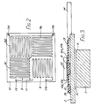
- the chip comprises an MR sensor (best seen in Figure 2) which includes a bridge 9 of known construction deposited on an oxidised layer of a silicon substrate 10.
- the bridge structure 9 is made by configuring a permalloy (Ni/Fe) film 11 to form four meander pattern resistors 9a, 9b, 9c and 9d.
- the nodes of the bridge 9 are connected to pads 11a, 11b, 11c and 11d.
- pads 11 may be connected, by means of an integral interconnection pattern, to solder elements 12a which are connected, through solder elements 12b, to metallisation 13 which is connected to terminal pins 14a-14b.
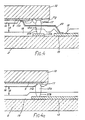
- pads 11 may be directly connected to the ceramic metallisation by a known wire-bonding technique as shown in Figure 4.
- substrate 2 is shown attached to the upper surface 4 of strap 5 by menas of a layer of solder 15.
- terminal pins 14a and 14c are connected respectively to negative and positive sides of a voltage source (not shown) and an analog output is developed across terminal pins 14b and 14d.
- the bridge structure 9 on its silicon substrate 10 is covered with an insulating passivation layer 16 (e.g. by a known technique).
- vias or voids 17 are left either at the locations of electrically isolated dummy pads 11g adjacent each of the wire bonded regions 18 ( Figure 4), or at the locations of the pads 11a-11d( Figure 4).
- Solder elements 12a are then deposited on the dummy pads 11g or pads 11a-11d, e.g. by vapour phase deposition through holes in a metal mask (not shown) aligned with dummy pads 11g or pads 11.
- solder is applied to each via 17 so as to leave an element 12a which extends a predetermined distance "a" above the outer surface of the insulation 16 so that, when the substrate 10 is inverted and placed on the substrate 2, the solder elements 12a support the substrate 10 with a clearance "a” between the outer surface of the insulating layer 16 and the upper surface of insulation 19 (on substrate 2).
- the substrate 2 and its metallisation 13 is covered with a layer of insulation 19 and, as shown in Figures 4 and 4a, vias or voids 17 are left in layer 19 at locations respectively corresponding with the positions of vias 17 in layer 16 (in other words, the vias 17 are a mirror image of one another).
- vias 17 in layer 19 are located over electrically isolated dummy pads 11h.
- Solder is then deposited in vias 17 to form elements 12b. This may be done in the same way as elements 12a were provided for the chip or screen-printed in paste form.
- a film or layer of solder 15 is also deposited (by a known technique) on the lower surface of substrate 2 (as shown in Figure 3). This film of solder 15 is intended to make contact with the upper surface 4 of the copper strap 5.
- Substrates 10 and 2 are then mounted on strap 4 so that the solder elements 12a and 12b are substantially aligned.
- the bridge substrate 9 has a substantially predetermined orientation with respect to (the direction of current flow in) copper strap 5.
- the bridge structure 9 is also substantially parallel with the upper surface 4 of strap 5.
- the sub-assembly shown in Figure 3 is then placed on a belt (not shown) of a chain belt furnace (not shown) which has a carefully-controlled time/temperature profile.
- the assembly is thereby transported at constant speed through the furnace whereby the solder elements 12a, 12b soften and fuse together to cause substrate 10 to adhere to substrate 2, to ensure a good electrical connection to be made between pads 11a-11d and metallisation 13 (connected to pins 14a-14d) i.e. where this is the case with the preferred arrangement shown in Figure 4a, and to cause substrate 2 to adhere to the upper surface 4 of copper strap 5 whilst leaving the bridge structure 9 positioned to a predetermined distance above surface 4.
- the bridge structure 9 is positioned as close as possible to the surface 4 of the copper strap 5 allowing for the intervening substrate, insulation and metallisation.
- the thickness of substrate 2 can be controlled to provide a required sensitivity whilst preventing any undesirable short circuits.
- the dimensions of the solder elements and the disposition or pattern of the vias 17 are selected or predetermined to assist in the final accurate positioning of the bridge structure, i.e. in a mass-production process.
- the elements 12a, 12b become molten, their surface tension provides a self-aligning function (within tolerable limits) and the degree of softening allows the substrate 10 to sag down onto the insulating layer 19 by the required amount, i.e. due to the carefully controlled time-temperature profile in the furnace.
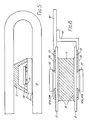
- FIG. 5 illustrates an alternative embodiment, partly in section, in which similar components have been given similar reference numerals.
- a similar silicon chip formed on a substrate 10 is mounted on a ceramic substrate 2 and is covered with a ceramic cap 3.
- the ceramic substrate 2 is mounted on a copper strap 5 which is bent back upon itself, as shown in the drawing, so as to contact the upper surface of the insulating cap 3.
- the sensing and power circuits are thereby electrically isolated from the strap 5.
- the "return path" of the strap 5 facilitates low current measurement since it increases the magnetic field in the vicinity of the bridge structure 9 for the same amount of current flowing through the strap 5.
- FIG. 6 illustrates a further embodiment in which similar components have been given similar reference numerals.
- substrates 2 and silicon chips formed on substrates 10 are mounted on opposite sides of a copper strap 5.
- the terminal pins 14a-14d of each device are connected in an anti-coincident mode wherein the responses of the devices to an external magnetic field (interference) cancel one another, whilst the responses of the devices to magnetic fields of opposite direction, i.e. due to current flow in the copper strap 5, reinforce one another to provide a sum output.
- a logic output triggered by a predetermined magnetic field can be achieved by utilising either (i) a logic circuit diffused into the substrate of the chip or (ii) a logic hybrid circuit assembled and bonded onto the ceramic substrate 2.
- the advantage of logic circuitry incorporated into the sensing device is a reduction of sense circuit connections from four to three, the incorporation of output signal conditioning (e.g. a hysteresis switch point) and the conditioning or stabilisation of a sensor drive power supply.
- output signal conditioning e.g. a hysteresis switch point
- Figure 7 illustrates an alternative, Barber-pole biased, bridge structure 9.
- the magnetoresistive element is configured in four meander pattern resistors, two of each polarity, sharing common interconnection pads 11b, 11c and 11d so as to provide a "push-pull" bridge format when pads 11a and 11d are commonly connected by metallisation 13.
- Certain portion of this bridge structure as illustrated by the magnified inserts, one of each polarity, show conductive stripes 21 (e.g. of aluminium) each having a predetermined angle of inclination.
- the shading on the stripes 21, which is in the same direction, is merely intended to distinguish the stripes 21 from the underlining magnetoresistive element, e.g. a permalloy stripe 11 in the drawing.
Landscapes
- Physics & Mathematics (AREA)
- General Physics & Mathematics (AREA)
- Measuring Magnetic Variables (AREA)
- Hall/Mr Elements (AREA)
- Measuring Instrument Details And Bridges, And Automatic Balancing Devices (AREA)
Applications Claiming Priority (2)
| Application Number | Priority Date | Filing Date | Title |
|---|---|---|---|
| GB8725467 | 1987-10-30 | ||
| GB878725467A GB8725467D0 (en) | 1987-10-30 | 1987-10-30 | Making current sensor |
Publications (2)
| Publication Number | Publication Date |
|---|---|
| EP0315358A2 true EP0315358A2 (de) | 1989-05-10 |
| EP0315358A3 EP0315358A3 (de) | 1991-05-02 |
Family
ID=10626183
Family Applications (1)
| Application Number | Title | Priority Date | Filing Date |
|---|---|---|---|
| EP19880310047 Withdrawn EP0315358A3 (de) | 1987-10-30 | 1988-10-26 | Verfahren zur Herstellung eines Stromsensors |
Country Status (4)
| Country | Link |
|---|---|
| US (1) | US4922606A (de) |
| EP (1) | EP0315358A3 (de) |
| CA (1) | CA1292082C (de) |
| GB (1) | GB8725467D0 (de) |
Cited By (6)
| Publication number | Priority date | Publication date | Assignee | Title |
|---|---|---|---|---|
| EP0703460A1 (de) * | 1994-09-26 | 1996-03-27 | CROUZET Automatismes | Magnetoresistiver Strommesser |
| DE10013345A1 (de) * | 2000-03-17 | 2001-10-04 | Sauer Danfoss Nordborg As Nord | Einrichtung zum Messen eines durch eine Leiterbahn fließenden elektrischen Stroms |
| EP1482314A1 (de) * | 1996-05-17 | 2004-12-01 | Formfactor, Inc. | Mikroelektronisches Federkontaktelement |
| US7073254B2 (en) | 1993-11-16 | 2006-07-11 | Formfactor, Inc. | Method for mounting a plurality of spring contact elements |
| WO2012007247A1 (de) | 2010-07-14 | 2012-01-19 | Siemens Aktiengesellschaft | Modul und anordnung zur messung eines hochfrequenzstroms durch einen leiter |
| EP2060923A3 (de) * | 2007-11-14 | 2013-02-27 | Robert Bosch Gmbh | Anordnung zur Messung eines elektrischen Stromes |
Families Citing this family (18)
| Publication number | Priority date | Publication date | Assignee | Title |
|---|---|---|---|---|
| JP3106541B2 (ja) * | 1991-04-15 | 2000-11-06 | 日本電気株式会社 | 磁気ヘッド駆動回路 |
| US6896826B2 (en) * | 1997-01-09 | 2005-05-24 | Advanced Technology Materials, Inc. | Aqueous cleaning composition containing copper-specific corrosion inhibitor for cleaning inorganic residues on semiconductor substrate |
| GB9813982D0 (en) * | 1998-06-30 | 1998-08-26 | Mem Limited | Residual current detection device |
| US6949927B2 (en) | 2001-08-27 | 2005-09-27 | International Rectifier Corporation | Magnetoresistive magnetic field sensors and motor control devices using same |
| US6717403B2 (en) * | 2001-09-06 | 2004-04-06 | Honeywell International Inc. | Method and system for improving the efficiency of the set and offset straps on a magnetic sensor |
| US6921965B1 (en) * | 2002-06-20 | 2005-07-26 | Silicon Magnetic Systems | Die surface magnetic field shield |
| US7259545B2 (en) * | 2003-02-11 | 2007-08-21 | Allegro Microsystems, Inc. | Integrated sensor |
| TWI227502B (en) | 2003-09-02 | 2005-02-01 | Ind Tech Res Inst | Precise multi-pole magnetic components and manufacturing method thereof |
| JP4433820B2 (ja) * | 2004-02-20 | 2010-03-17 | Tdk株式会社 | 磁気検出素子およびその形成方法ならびに磁気センサ、電流計 |
| US7768083B2 (en) * | 2006-01-20 | 2010-08-03 | Allegro Microsystems, Inc. | Arrangements for an integrated sensor |
| US8269319B2 (en) * | 2006-10-13 | 2012-09-18 | Tessera, Inc. | Collective and synergistic MRAM shields |
| US7816905B2 (en) * | 2008-06-02 | 2010-10-19 | Allegro Microsystems, Inc. | Arrangements for a current sensing circuit and integrated current sensor |
| US8525514B2 (en) * | 2010-03-19 | 2013-09-03 | Memsic, Inc. | Magnetometer |
| JP5579218B2 (ja) * | 2012-03-28 | 2014-08-27 | 株式会社東芝 | 圧力検知素子の製造方法 |
| US9976876B2 (en) | 2015-11-24 | 2018-05-22 | Allegro Microsystems, Llc | Methods and apparatus for phase selection in ring magnet sensing |
| US10935612B2 (en) | 2018-08-20 | 2021-03-02 | Allegro Microsystems, Llc | Current sensor having multiple sensitivity ranges |
| US11567108B2 (en) | 2021-03-31 | 2023-01-31 | Allegro Microsystems, Llc | Multi-gain channels for multi-range sensor |
| US11994541B2 (en) | 2022-04-15 | 2024-05-28 | Allegro Microsystems, Llc | Current sensor assemblies for low currents |
Family Cites Families (12)
| Publication number | Priority date | Publication date | Assignee | Title |
|---|---|---|---|---|
| FR2453463A2 (fr) * | 1979-04-06 | 1980-10-31 | Cii Honeywell Bull | Procede de generation d'un champ d'induction magnetique dans un milieu magnetique |
| CH651151A5 (de) * | 1979-11-27 | 1985-08-30 | Landis & Gyr Ag | Messwandler zum messen eines insbesondere von einem messstrom erzeugten magnetfeldes. |
| NL7908611A (nl) * | 1979-11-28 | 1981-07-01 | Philips Nv | Geintegreerde magneetkopconstructie. |
| JPS5898821A (ja) * | 1981-12-09 | 1983-06-11 | Comput Basic Mach Technol Res Assoc | 薄膜磁気ヘツドの製造方法 |
| US4589043A (en) * | 1982-08-31 | 1986-05-13 | Grundtner Matthias J | Magnetic head having a thermoplastic or a thermosetting plastic housing |
| JPS5979417A (ja) * | 1982-10-28 | 1984-05-08 | Sony Corp | 磁気ヘツド装置 |
| JPS59104717A (ja) * | 1982-12-08 | 1984-06-16 | Comput Basic Mach Technol Res Assoc | 薄膜磁気ヘツドおよびその製造方法 |
| US4571651A (en) * | 1983-10-14 | 1986-02-18 | Applied Magnetics Corporation | Method of manufacturing a magnetic head assembly and product |
| US4546541A (en) * | 1983-10-14 | 1985-10-15 | Applied Magnetics Corporation | Method of attaching electrical conductors to thin film magnetic transducer |
| JPS61126618A (ja) * | 1984-11-22 | 1986-06-14 | Nippon Telegr & Teleph Corp <Ntt> | 磁気抵抗効果薄膜ヘツド |
| US4783711A (en) * | 1985-07-12 | 1988-11-08 | Hitachi, Ltd. | Magnetoresistive sensor having magnetic shields of ferrite |
| US4652954A (en) * | 1985-10-24 | 1987-03-24 | International Business Machines | Method for making a thin film magnetic head |
-
1987
- 1987-10-30 GB GB878725467A patent/GB8725467D0/en active Pending
-
1988
- 1988-10-18 US US07/259,223 patent/US4922606A/en not_active Expired - Fee Related
- 1988-10-25 CA CA000581202A patent/CA1292082C/en not_active Expired - Lifetime
- 1988-10-26 EP EP19880310047 patent/EP0315358A3/de not_active Withdrawn
Cited By (10)
| Publication number | Priority date | Publication date | Assignee | Title |
|---|---|---|---|---|
| US7073254B2 (en) | 1993-11-16 | 2006-07-11 | Formfactor, Inc. | Method for mounting a plurality of spring contact elements |
| EP0703460A1 (de) * | 1994-09-26 | 1996-03-27 | CROUZET Automatismes | Magnetoresistiver Strommesser |
| FR2725029A1 (fr) * | 1994-09-26 | 1996-03-29 | Crouzet Automatismes | Capteur de courant a magnetoresistance |
| EP1482314A1 (de) * | 1996-05-17 | 2004-12-01 | Formfactor, Inc. | Mikroelektronisches Federkontaktelement |
| DE10013345A1 (de) * | 2000-03-17 | 2001-10-04 | Sauer Danfoss Nordborg As Nord | Einrichtung zum Messen eines durch eine Leiterbahn fließenden elektrischen Stroms |
| US6768322B2 (en) | 2000-03-17 | 2004-07-27 | Sauer-Danfoss Holding A/S | Device for measuring an electrical current that flows through a strip conductor |
| DE10013345B4 (de) * | 2000-03-17 | 2004-08-26 | Sauer-Danfoss Holding Aps | Einrichtung zum Messen eines durch eine Leiterbahn fließenden elektrischen Stroms und deren Anwendung |
| EP2060923A3 (de) * | 2007-11-14 | 2013-02-27 | Robert Bosch Gmbh | Anordnung zur Messung eines elektrischen Stromes |
| WO2012007247A1 (de) | 2010-07-14 | 2012-01-19 | Siemens Aktiengesellschaft | Modul und anordnung zur messung eines hochfrequenzstroms durch einen leiter |
| DE102010027130A1 (de) | 2010-07-14 | 2012-01-19 | Siemens Aktiengesellschaft | Modul und Anordnung zur Messung eines Hochfrequenzstroms durch einen Leiter |
Also Published As
| Publication number | Publication date |
|---|---|
| CA1292082C (en) | 1991-11-12 |
| EP0315358A3 (de) | 1991-05-02 |
| GB8725467D0 (en) | 1987-12-02 |
| US4922606A (en) | 1990-05-08 |
Similar Documents
| Publication | Publication Date | Title |
|---|---|---|
| US4922606A (en) | Method of making a current sensor | |
| US4251795A (en) | Semiconductor magnetoresistive element having a differential effect | |
| EP1107328B1 (de) | Stromdetektor mit einer Hall-Effekt-Anordnung | |
| US4320655A (en) | Quantity of flow meter | |
| KR20000029928A (ko) | 자기전류센서 | |
| US6734671B2 (en) | Magnetic sensor and manufacturing method therefor | |
| US6769166B1 (en) | Method of making an electrical current sensor | |
| US6812687B1 (en) | Semiconductor current detector of improved noise immunity | |
| EP1399748B1 (de) | Halbzeug für einen sensor zum messen eines magnetischen feldes | |
| US6184680B1 (en) | Magnetic field sensor with components formed on a flexible substrate | |
| EP1974223B1 (de) | Anordnungen für einen integrierten Sensor | |
| US4401966A (en) | Magnetoelectric transducer and fabrication method therefor | |
| JPH0781877B2 (ja) | 磁界検知装置のためのパッケージ | |
| JPH10142303A (ja) | 較正中にレーザ・トリミングするために透明プレートに取り付けられた構成部品を備えた磁気センサ | |
| JPH03505501A (ja) | 磁気抵抗による垂直記録用の磁気読取りヘッド及び当該ヘッドの製造方法 | |
| JP2006242946A (ja) | 表面実装式集積電流センサ | |
| JP2001339109A (ja) | ホ−ル素子を備えた電流検出装置 | |
| KR100459361B1 (ko) | 자전 변환 소자 및 그의 제조 방법 | |
| Bajorek et al. | A permalloy current sensor | |
| JP2576763B2 (ja) | 強磁性磁気抵抗素子 | |
| WO2022085319A1 (ja) | 磁気センサパッケージ | |
| JPH10282156A (ja) | 電流センサー | |
| EP4597121A1 (de) | Stromwandler mit tmr-magnetfeldsensor | |
| JP2610083B2 (ja) | 強磁性体磁気抵抗素子 | |
| JP2715016B2 (ja) | ホール素子およびホール素子の製造方法 |
Legal Events
| Date | Code | Title | Description |
|---|---|---|---|
| PUAI | Public reference made under article 153(3) epc to a published international application that has entered the european phase |
Free format text: ORIGINAL CODE: 0009012 |
|
| AK | Designated contracting states |
Kind code of ref document: A2 Designated state(s): AT BE CH DE ES FR GB GR IT LI LU NL SE |
|
| 17P | Request for examination filed |
Effective date: 19891102 |
|
| PUAL | Search report despatched |
Free format text: ORIGINAL CODE: 0009013 |
|
| AK | Designated contracting states |
Kind code of ref document: A3 Designated state(s): AT BE CH DE ES FR GB GR IT LI LU NL SE |
|
| STAA | Information on the status of an ep patent application or granted ep patent |
Free format text: STATUS: THE APPLICATION IS DEEMED TO BE WITHDRAWN |
|
| 18D | Application deemed to be withdrawn |
Effective date: 19911103 |