EP0317015B1 - Réglage du courant de repos pour un circuit amplificateur - Google Patents
Réglage du courant de repos pour un circuit amplificateur Download PDFInfo
- Publication number
- EP0317015B1 EP0317015B1 EP88202545A EP88202545A EP0317015B1 EP 0317015 B1 EP0317015 B1 EP 0317015B1 EP 88202545 A EP88202545 A EP 88202545A EP 88202545 A EP88202545 A EP 88202545A EP 0317015 B1 EP0317015 B1 EP 0317015B1
- Authority
- EP
- European Patent Office
- Prior art keywords
- transistor
- transistors
- coupled
- amplifier circuit
- conductivity type
- Prior art date
- Legal status (The legal status is an assumption and is not a legal conclusion. Google has not performed a legal analysis and makes no representation as to the accuracy of the status listed.)
- Expired - Lifetime
Links
- 238000000034 method Methods 0.000 description 3
- 230000003071 parasitic effect Effects 0.000 description 3
- 230000000295 complement effect Effects 0.000 description 1
- 230000001419 dependent effect Effects 0.000 description 1
- 230000002349 favourable effect Effects 0.000 description 1
- 238000009413 insulation Methods 0.000 description 1
- 230000010354 integration Effects 0.000 description 1
- 239000000758 substrate Substances 0.000 description 1
Images
Classifications
-
- H—ELECTRICITY
- H03—ELECTRONIC CIRCUITRY
- H03F—AMPLIFIERS
- H03F3/00—Amplifiers with only discharge tubes or only semiconductor devices as amplifying elements
- H03F3/30—Single-ended push-pull [SEPP] amplifiers; Phase-splitters therefor
- H03F3/3001—Single-ended push-pull [SEPP] amplifiers; Phase-splitters therefor with field-effect transistors
- H03F3/301—CMOS common drain output SEPP amplifiers
- H03F3/3011—CMOS common drain output SEPP amplifiers with asymmetrical driving of the end stage
-
- H—ELECTRICITY
- H03—ELECTRONIC CIRCUITRY
- H03F—AMPLIFIERS
- H03F3/00—Amplifiers with only discharge tubes or only semiconductor devices as amplifying elements
- H03F3/30—Single-ended push-pull [SEPP] amplifiers; Phase-splitters therefor
- H03F3/3069—Single-ended push-pull [SEPP] amplifiers; Phase-splitters therefor the emitters of complementary power transistors being connected to the output
- H03F3/3071—Single-ended push-pull [SEPP] amplifiers; Phase-splitters therefor the emitters of complementary power transistors being connected to the output with asymmetrical driving of the end stage
Definitions
- the invention relates to an amplifier circuit comprising an input terminal, a series arrangement of a first transistor of a first conductivity type and a second transistor of a second conductivity type both arranged as diodes, and a series arrangement of a third transistor of the first conductivity type and a fourth transistor of the second conductivity type, each transistor having a first and a second main electrode and a control electrode, the control electrodes of the first and the second transistor being interconnected, the first main electrode of the first transistor being coupled to the control electrode of the fourth transistor, the first main electrode of the second transistor being coupled to the control electrode of the third transistor, and the intercoupled first main electrodes of the third and the fourth transistor being also coupled to an output terminal.
- the first main electrode is the emitter if bipolar transistors are concerned and the source if unipolar transistors (such as MOS transistors and JFETs) are concerned.
- the second main electrode (that is to say, the collector or drain) of the first transistor is coupled to the associated control electrode of this transistor.
- the second main electrode of the second transistor is coupled to the associated control electrode of this transistor.
- the control electrodes of the first and the second transistor are interconnected.
- the quiescent output current I out is small as compared with the input current I in .
- n must be large.
- the first and second transistors arranged as diodes must be larger than the third and the fourth transistor.
- the third and fourth transistors are large anyway because they must be able to supply the large output current required for a class AB amplifier.
- the amplifier circuit thus realized occupies an undesirably large part of the chip surface area. Moreover, the first and second transistors then have a large parasitic capacitance with respect to the substrate.
- a drawback of the second solution is that the resistance must be large so that a large chip surface area is required in the case of integration and moreover the output impedance of the amplifier circuit increases.
- the invention proposes to provide an amplifier circuit occupying a small chip surface area and having a small parasitic capacitance and a considerable insensitivity to threshold voltages.
- the amplifier circuit according to the invention is characterized in that a series arrangement of an impedance and a fifth transistor of the second conductivity type is arranged parallel to the series arrangement of the first and the second transistor, the control electrode of the second transistor being coupled to the control electrode of the fifth transistor, the first main electrode of the first transistor being coupled via the impedance to the control electrode of the first transistor and the first main electrode of the second transistor being coupled to the first main electrode of the fifth transistor.
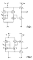
- Figure 1 shows an amplifier circuit in the form of a class AB output stage, comprising a series arrangement of a first and a second transistor T1 and T2, respectively, both in the form of a MOSFET, coupled between the terminals 1 and 2.
- the first transistor T1 is a mosfet of the n-type and the second transistor is a mosfet of the p-type. Both transistors are arranged as diodes. This means that the control electrode (gate) of each of the two transistors is coupled to the one (namely the second) main electrode (the drain) of the relevant transistor.
- a series arrangement of a third transistor T3 and a fourth transistor T4 is provided between terminals 3 and 4.
- the third transistor is a mosfet of the n-type and the fourth transistor is a mosfet of the p-type.
- the source-main electrodes of the two transistors T3 and T4 are coupled together and are coupled to an output terminal 5 of the amplifier circuit.
- the source-main electrode of the transistor T2 is coupled to the control electrode of the transistor T3.
- the source-main electrode of the transistor T1 is coupled via an impedance in the form of a resistor R to the control electrode of the transistor T4.
- a series arrangement of the impedance R and a fifth transistor T5 is arranged parallel to the series arrangement of the transistors T1 and T2 between the terminals 1 and 2.
- the source-main electrodes of the transistors T2 and T5 are coupled together and to the terminal 1.
- the control electrodes (gates) of the transistors T2 and T5 are coupled together.
- the source-main electrode of transistor T1 is coupled to the terminal 2.
- Quiescent currents I in and I out flow in the circuits.
- the quiescent input current I in flows from terminal 1 to terminal 2 and spreads over the two parallel-arranged circuits constituted by the transistors T1 and T2 through which a quiescent current I12 flows and constituted by the transistor T5 and the impedance R through which a quiescent current I r flows.
- the quiescent output current I out flows from terminal 3 via the transistors T3 and T4 to terminal 4.
- the quiescent current I in is supplied by a current source (not shown) which is connected to one of the terminals 1 or 2.
- An input signal to be amplified by the amplifier circuit may be applied to one of the terminals 1 or 2, or to the terminal 6 being the junction point between the drain-main electrodes of the transistors T1 and T2.
- the (current-) amplified output signal is present at the output terminal 5.
- the terminals 3 and 4 are coupled to suitable supply voltages.
- the transistors T1 and T2 create a voltage drop whose value is determined by the threshold voltages and the gain factors of T1 and T2 and the current (I12) through T1 and T2. A voltage drop which is subtracted from the voltage drop across T1 and T2 is created across the resistor R.
- Figure 2 shows a second embodiment bearing great resemblance to the embodiment of Figure 1.
- the transistors T1 and T2 are arranged in the reverse order in the circuit between the terminals 1 and 2.
- the transistors are of a different conductivity type.
- Transistor T1 is of the p-type and transistor T2 is of the n-type.
- the transistor T5 and the impedance R have a reversed order and the transistor T5 is of the different conductivity type (namely the n-type).
- the operation of the circuit of Figure 2 is not principally different from that of the circuit of Figure 1 so that it does not require any further explanation.
- the advantages are:
- the invention is not limited to the amplifier circuit shown in the embodiments.
- the invention can also be used for those amplifier circuits which differ from the embodiments shown in aspects not relating to the invention.
- an amplifier circuit in which the transistors are in the form of bipolar transistors is also possible.
Landscapes
- Engineering & Computer Science (AREA)
- Power Engineering (AREA)
- Amplifiers (AREA)
Claims (2)
- Circuit amplificateur comprenant une borne d'entrée (1, 2, 6), un montage en série d'un premier transistor (T₁), d'un premier type de conductivité et d'un deuxième transistor (T₂) d'un second type de conductivité, agencés tous deux comme des diodes, et un montage en série d'un troisième transistor (T₃) du premier type de conductivité et d'un quatrième transistor (T₄) du second type de conductivité, chaque transistor comportant une première et une seconde électrode principale, ainsi qu'une électrode de commande, les électrodes de commande du premier et du deuxième transistor étant interconnectées, la première électrode principale du premier transistor étant couplée à l'électrode de commande du quatrième tansistor, la première électrode principale du deuxième transistor étant couplée à l'électrode de commande du troisième transistor, et les premières électrodes principales interconnectées du troisième et du quatrième transistor étant également couplées à une borne de sortie (5), caractérisé en ce qu'un montage en série d'une impédance et d'un cinquième transistor (T₅) du second type de conductivité est disposé en parallèle avec le montage en série du premier et du deuxième transistor, l'électrode de commande du deuxième transistor étant couplée à l'électrode de commande du cinquième transistor, la première électrode principale du premier transistor étant couplée, par l'intermédiaire de l'impédance (R), à l'électrode de commande du quatrième transistor et la première électrode principale du deuxième transistor étant couplée à la première électrode principale du cinquième transistor.
- Circuit amplificateur suivant la revendication 1, caractérisé en ce que l'impédance (R) est une résistance ayant une valeur R qui est égale à

Applications Claiming Priority (2)
| Application Number | Priority Date | Filing Date | Title |
|---|---|---|---|
| NL8702778A NL8702778A (nl) | 1987-11-20 | 1987-11-20 | Ruststroominstelling voor een versterkerschakeling. |
| NL8702778 | 1987-11-20 |
Publications (2)
| Publication Number | Publication Date |
|---|---|
| EP0317015A1 EP0317015A1 (fr) | 1989-05-24 |
| EP0317015B1 true EP0317015B1 (fr) | 1992-09-02 |
Family
ID=19850944
Family Applications (1)
| Application Number | Title | Priority Date | Filing Date |
|---|---|---|---|
| EP88202545A Expired - Lifetime EP0317015B1 (fr) | 1987-11-20 | 1988-11-15 | Réglage du courant de repos pour un circuit amplificateur |
Country Status (6)
| Country | Link |
|---|---|
| US (1) | US4868518A (fr) |
| EP (1) | EP0317015B1 (fr) |
| JP (1) | JPH01162005A (fr) |
| KR (1) | KR970005290B1 (fr) |
| DE (1) | DE3874293T2 (fr) |
| NL (1) | NL8702778A (fr) |
Families Citing this family (6)
| Publication number | Priority date | Publication date | Assignee | Title |
|---|---|---|---|---|
| US5057789A (en) * | 1990-07-31 | 1991-10-15 | At&T Bell Laboratories | Class AB CMOS amplifier |
| US5177374A (en) * | 1990-10-03 | 1993-01-05 | International Business Machines Corporation | Current mode gate drive for power mos transistors |
| US5689211A (en) * | 1996-02-14 | 1997-11-18 | Lucent Technologies Inc. | Quiescent current control for the output stage of an amplifier |
| IT1291676B1 (it) * | 1997-04-28 | 1999-01-19 | Sgs Thomson Microelectronics | Stadio di uscita a cmos esente da fenomeni di deriva |
| FR2829886B1 (fr) | 2001-09-18 | 2005-09-30 | St Microelectronics Sa | Circuit amplificateur en classe ab |
| US20070096821A1 (en) * | 2005-11-03 | 2007-05-03 | Samsung Electronics Co., Ltd. | Wide-band amplifier |
Family Cites Families (3)
| Publication number | Priority date | Publication date | Assignee | Title |
|---|---|---|---|---|
| US3701031A (en) * | 1970-08-26 | 1972-10-24 | Motorola Inc | Complementary power amplifier |
| US4038607A (en) * | 1976-08-23 | 1977-07-26 | Rca Corporation | Complementary field effect transistor amplifier |
| US4467288A (en) * | 1982-01-05 | 1984-08-21 | Strickland James C | Distortion-free complemented error feedback amplifier and method |
-
1987
- 1987-11-20 NL NL8702778A patent/NL8702778A/nl not_active Application Discontinuation
-
1988
- 1988-10-31 US US07/264,752 patent/US4868518A/en not_active Expired - Fee Related
- 1988-11-15 EP EP88202545A patent/EP0317015B1/fr not_active Expired - Lifetime
- 1988-11-15 DE DE8888202545T patent/DE3874293T2/de not_active Expired - Fee Related
- 1988-11-17 KR KR1019880015108A patent/KR970005290B1/ko not_active Expired - Lifetime
- 1988-11-18 JP JP63290303A patent/JPH01162005A/ja active Pending
Non-Patent Citations (1)
| Title |
|---|
| P.R. Gray et al: "Analysis and Design of Analog Integrated Circuits", 1984, John Wiley, New York, US, page 335 * |
Also Published As
| Publication number | Publication date |
|---|---|
| KR890009071A (ko) | 1989-07-13 |
| DE3874293D1 (de) | 1992-10-08 |
| EP0317015A1 (fr) | 1989-05-24 |
| US4868518A (en) | 1989-09-19 |
| JPH01162005A (ja) | 1989-06-26 |
| KR970005290B1 (ko) | 1997-04-15 |
| NL8702778A (nl) | 1989-06-16 |
| DE3874293T2 (de) | 1993-03-25 |
Similar Documents
| Publication | Publication Date | Title |
|---|---|---|
| US5734296A (en) | Low voltage operational amplifier input stage and method | |
| US5519309A (en) | Voltage to current converter with extended dynamic range | |
| US3835410A (en) | Current amplifier | |
| US5699015A (en) | Low voltage operational amplifier and method | |
| US5266887A (en) | Bidirectional voltage to current converter | |
| US3953807A (en) | Current amplifier | |
| US5798673A (en) | Low voltage operational amplifier bias circuit and method | |
| CA1078469A (fr) | Amplificateur differentiel | |
| EP0123275B1 (fr) | Circuit amplificateur opérationnel | |
| US3832644A (en) | Semiconductor electronic circuit with semiconductor bias circuit | |
| EP0209987A2 (fr) | Amplificateur tampon à gain unité | |
| EP0155720B1 (fr) | Dispositif de source de courant en cascade | |
| EP0419819A1 (fr) | Miroir de courant | |
| US4574233A (en) | High impedance current source | |
| US5808501A (en) | Voltage level shifter and method | |
| EP0056809A1 (fr) | Source de courant cascode. | |
| EP0317015A1 (fr) | Réglage du courant de repos pour un circuit amplificateur | |
| EP0164182B1 (fr) | Etage d'entrée JFET à résistance de charge active | |
| EP0522786A1 (fr) | Amplification du type classe A avec polarisation glissante | |
| US4194166A (en) | Differential amplifier with a current mirror circuit | |
| US4398160A (en) | Current mirror circuits with field effect transistor feedback | |
| KR930007295B1 (ko) | 증폭기 장치 | |
| US3942129A (en) | Controlled gain amplifier | |
| US4117416A (en) | Current mirror amplifiers with programmable current gains | |
| US5343165A (en) | Amplifier having a symmetrical output characteristic |
Legal Events
| Date | Code | Title | Description |
|---|---|---|---|
| PUAI | Public reference made under article 153(3) epc to a published international application that has entered the european phase |
Free format text: ORIGINAL CODE: 0009012 |
|
| AK | Designated contracting states |
Kind code of ref document: A1 Designated state(s): DE FR GB IT NL |
|
| 17P | Request for examination filed |
Effective date: 19891122 |
|
| 17Q | First examination report despatched |
Effective date: 19911018 |
|
| GRAA | (expected) grant |
Free format text: ORIGINAL CODE: 0009210 |
|
| AK | Designated contracting states |
Kind code of ref document: B1 Designated state(s): DE FR GB IT NL |
|
| PG25 | Lapsed in a contracting state [announced via postgrant information from national office to epo] |
Ref country code: NL Effective date: 19920902 |
|
| REF | Corresponds to: |
Ref document number: 3874293 Country of ref document: DE Date of ref document: 19921008 |
|
| ITF | It: translation for a ep patent filed | ||
| ET | Fr: translation filed | ||
| NLV1 | Nl: lapsed or annulled due to failure to fulfill the requirements of art. 29p and 29m of the patents act | ||
| PLBE | No opposition filed within time limit |
Free format text: ORIGINAL CODE: 0009261 |
|
| STAA | Information on the status of an ep patent application or granted ep patent |
Free format text: STATUS: NO OPPOSITION FILED WITHIN TIME LIMIT |
|
| 26N | No opposition filed | ||
| ITPR | It: changes in ownership of a european patent |
Owner name: CAMBIO RAGIONE SOCIALE;PHILIPS ELECTRONICS N.V. |
|
| REG | Reference to a national code |
Ref country code: FR Ref legal event code: CD |
|
| PGFP | Annual fee paid to national office [announced via postgrant information from national office to epo] |
Ref country code: GB Payment date: 19961101 Year of fee payment: 9 |
|
| PGFP | Annual fee paid to national office [announced via postgrant information from national office to epo] |
Ref country code: FR Payment date: 19961119 Year of fee payment: 9 |
|
| PGFP | Annual fee paid to national office [announced via postgrant information from national office to epo] |
Ref country code: DE Payment date: 19970127 Year of fee payment: 9 |
|
| PG25 | Lapsed in a contracting state [announced via postgrant information from national office to epo] |
Ref country code: GB Free format text: LAPSE BECAUSE OF NON-PAYMENT OF DUE FEES Effective date: 19971115 |
|
| PG25 | Lapsed in a contracting state [announced via postgrant information from national office to epo] |
Ref country code: FR Free format text: THE PATENT HAS BEEN ANNULLED BY A DECISION OF A NATIONAL AUTHORITY Effective date: 19971130 |
|
| GBPC | Gb: european patent ceased through non-payment of renewal fee |
Effective date: 19971115 |
|
| PG25 | Lapsed in a contracting state [announced via postgrant information from national office to epo] |
Ref country code: DE Free format text: LAPSE BECAUSE OF NON-PAYMENT OF DUE FEES Effective date: 19980801 |
|
| REG | Reference to a national code |
Ref country code: FR Ref legal event code: ST |
|
| PG25 | Lapsed in a contracting state [announced via postgrant information from national office to epo] |
Ref country code: IT Free format text: LAPSE BECAUSE OF NON-PAYMENT OF DUE FEES;WARNING: LAPSES OF ITALIAN PATENTS WITH EFFECTIVE DATE BEFORE 2007 MAY HAVE OCCURRED AT ANY TIME BEFORE 2007. THE CORRECT EFFECTIVE DATE MAY BE DIFFERENT FROM THE ONE RECORDED. Effective date: 20051115 |