EP0317256A2 - Ein Substrat für gedruckte Schaltungen - Google Patents
Ein Substrat für gedruckte Schaltungen Download PDFInfo
- Publication number
- EP0317256A2 EP0317256A2 EP88310759A EP88310759A EP0317256A2 EP 0317256 A2 EP0317256 A2 EP 0317256A2 EP 88310759 A EP88310759 A EP 88310759A EP 88310759 A EP88310759 A EP 88310759A EP 0317256 A2 EP0317256 A2 EP 0317256A2
- Authority
- EP
- European Patent Office
- Prior art keywords
- printed circuit
- substrate
- circuit according
- conductive material
- dielectric
- Prior art date
- Legal status (The legal status is an assumption and is not a legal conclusion. Google has not performed a legal analysis and makes no representation as to the accuracy of the status listed.)
- Withdrawn
Links
Images
Classifications
-
- B—PERFORMING OPERATIONS; TRANSPORTING
- B23—MACHINE TOOLS; METAL-WORKING NOT OTHERWISE PROVIDED FOR
- B23Q—DETAILS, COMPONENTS, OR ACCESSORIES FOR MACHINE TOOLS, e.g. ARRANGEMENTS FOR COPYING OR CONTROLLING; MACHINE TOOLS IN GENERAL CHARACTERISED BY THE CONSTRUCTION OF PARTICULAR DETAILS OR COMPONENTS; COMBINATIONS OR ASSOCIATIONS OF METAL-WORKING MACHINES, NOT DIRECTED TO A PARTICULAR RESULT
- B23Q3/00—Devices holding, supporting, or positioning work or tools, of a kind normally removable from the machine
- B23Q3/02—Devices holding, supporting, or positioning work or tools, of a kind normally removable from the machine for mounting on a work-table, tool-slide, or analogous part
-
- H—ELECTRICITY
- H01—ELECTRIC ELEMENTS
- H01C—RESISTORS
- H01C7/00—Non-adjustable resistors formed as one or more layers or coatings; Non-adjustable resistors made from powdered conducting material or powdered semi-conducting material with or without insulating material
- H01C7/22—Elongated resistive element being bent or curved, e.g. sinusoidal, helical
-
- H—ELECTRICITY
- H05—ELECTRIC TECHNIQUES NOT OTHERWISE PROVIDED FOR
- H05K—PRINTED CIRCUITS; CASINGS OR CONSTRUCTIONAL DETAILS OF ELECTRIC APPARATUS; MANUFACTURE OF ASSEMBLAGES OF ELECTRICAL COMPONENTS
- H05K1/00—Printed circuits
- H05K1/02—Details
- H05K1/03—Use of materials for the substrate
- H05K1/0313—Organic insulating material
- H05K1/0353—Organic insulating material consisting of two or more materials, e.g. two or more polymers, polymer + filler, + reinforcement
-
- H—ELECTRICITY
- H05—ELECTRIC TECHNIQUES NOT OTHERWISE PROVIDED FOR
- H05K—PRINTED CIRCUITS; CASINGS OR CONSTRUCTIONAL DETAILS OF ELECTRIC APPARATUS; MANUFACTURE OF ASSEMBLAGES OF ELECTRICAL COMPONENTS
- H05K1/00—Printed circuits
- H05K1/16—Printed circuits incorporating printed electric components, e.g. printed resistors, capacitors or inductors
- H05K1/162—Printed circuits incorporating printed electric components, e.g. printed resistors, capacitors or inductors incorporating printed capacitors
-
- H—ELECTRICITY
- H05—ELECTRIC TECHNIQUES NOT OTHERWISE PROVIDED FOR
- H05K—PRINTED CIRCUITS; CASINGS OR CONSTRUCTIONAL DETAILS OF ELECTRIC APPARATUS; MANUFACTURE OF ASSEMBLAGES OF ELECTRICAL COMPONENTS
- H05K1/00—Printed circuits
- H05K1/16—Printed circuits incorporating printed electric components, e.g. printed resistors, capacitors or inductors
- H05K1/167—Printed circuits incorporating printed electric components, e.g. printed resistors, capacitors or inductors incorporating printed resistors
-
- H—ELECTRICITY
- H05—ELECTRIC TECHNIQUES NOT OTHERWISE PROVIDED FOR
- H05K—PRINTED CIRCUITS; CASINGS OR CONSTRUCTIONAL DETAILS OF ELECTRIC APPARATUS; MANUFACTURE OF ASSEMBLAGES OF ELECTRICAL COMPONENTS
- H05K2201/00—Indexing scheme relating to printed circuits covered by H05K1/00
- H05K2201/01—Dielectrics
- H05K2201/0104—Properties and characteristics in general
- H05K2201/0116—Porous, e.g. foam
-
- H—ELECTRICITY
- H05—ELECTRIC TECHNIQUES NOT OTHERWISE PROVIDED FOR
- H05K—PRINTED CIRCUITS; CASINGS OR CONSTRUCTIONAL DETAILS OF ELECTRIC APPARATUS; MANUFACTURE OF ASSEMBLAGES OF ELECTRICAL COMPONENTS
- H05K2201/00—Indexing scheme relating to printed circuits covered by H05K1/00
- H05K2201/01—Dielectrics
- H05K2201/0137—Materials
- H05K2201/015—Fluoropolymer, e.g. polytetrafluoroethylene [PTFE]
-
- H—ELECTRICITY
- H05—ELECTRIC TECHNIQUES NOT OTHERWISE PROVIDED FOR
- H05K—PRINTED CIRCUITS; CASINGS OR CONSTRUCTIONAL DETAILS OF ELECTRIC APPARATUS; MANUFACTURE OF ASSEMBLAGES OF ELECTRICAL COMPONENTS
- H05K2201/00—Indexing scheme relating to printed circuits covered by H05K1/00
- H05K2201/01—Dielectrics
- H05K2201/0183—Dielectric layers
- H05K2201/0187—Dielectric layers with regions of different dielectrics in the same layer, e.g. in a printed capacitor for locally changing the dielectric properties
-
- H—ELECTRICITY
- H05—ELECTRIC TECHNIQUES NOT OTHERWISE PROVIDED FOR
- H05K—PRINTED CIRCUITS; CASINGS OR CONSTRUCTIONAL DETAILS OF ELECTRIC APPARATUS; MANUFACTURE OF ASSEMBLAGES OF ELECTRICAL COMPONENTS
- H05K2201/00—Indexing scheme relating to printed circuits covered by H05K1/00
- H05K2201/02—Fillers; Particles; Fibers; Reinforcement materials
- H05K2201/0203—Fillers and particles
- H05K2201/0206—Materials
- H05K2201/0209—Inorganic, non-metallic particles
-
- H—ELECTRICITY
- H05—ELECTRIC TECHNIQUES NOT OTHERWISE PROVIDED FOR
- H05K—PRINTED CIRCUITS; CASINGS OR CONSTRUCTIONAL DETAILS OF ELECTRIC APPARATUS; MANUFACTURE OF ASSEMBLAGES OF ELECTRICAL COMPONENTS
- H05K2201/00—Indexing scheme relating to printed circuits covered by H05K1/00
- H05K2201/03—Conductive materials
- H05K2201/032—Materials
- H05K2201/0323—Carbon
-
- H—ELECTRICITY
- H05—ELECTRIC TECHNIQUES NOT OTHERWISE PROVIDED FOR
- H05K—PRINTED CIRCUITS; CASINGS OR CONSTRUCTIONAL DETAILS OF ELECTRIC APPARATUS; MANUFACTURE OF ASSEMBLAGES OF ELECTRICAL COMPONENTS
- H05K2201/00—Indexing scheme relating to printed circuits covered by H05K1/00
- H05K2201/03—Conductive materials
- H05K2201/0332—Structure of the conductor
- H05K2201/0364—Conductor shape
- H05K2201/0376—Flush conductors, i.e. flush with the surface of the printed circuit
-
- H—ELECTRICITY
- H05—ELECTRIC TECHNIQUES NOT OTHERWISE PROVIDED FOR
- H05K—PRINTED CIRCUITS; CASINGS OR CONSTRUCTIONAL DETAILS OF ELECTRIC APPARATUS; MANUFACTURE OF ASSEMBLAGES OF ELECTRICAL COMPONENTS
- H05K2201/00—Indexing scheme relating to printed circuits covered by H05K1/00
- H05K2201/08—Magnetic details
- H05K2201/083—Magnetic materials
- H05K2201/086—Magnetic materials for inductive purposes, e.g. printed inductor with ferrite core
-
- H—ELECTRICITY
- H05—ELECTRIC TECHNIQUES NOT OTHERWISE PROVIDED FOR
- H05K—PRINTED CIRCUITS; CASINGS OR CONSTRUCTIONAL DETAILS OF ELECTRIC APPARATUS; MANUFACTURE OF ASSEMBLAGES OF ELECTRICAL COMPONENTS
- H05K2201/00—Indexing scheme relating to printed circuits covered by H05K1/00
- H05K2201/09—Shape and layout
- H05K2201/09209—Shape and layout details of conductors
- H05K2201/095—Conductive through-holes or vias
- H05K2201/09563—Metal filled via
-
- H—ELECTRICITY
- H05—ELECTRIC TECHNIQUES NOT OTHERWISE PROVIDED FOR
- H05K—PRINTED CIRCUITS; CASINGS OR CONSTRUCTIONAL DETAILS OF ELECTRIC APPARATUS; MANUFACTURE OF ASSEMBLAGES OF ELECTRICAL COMPONENTS
- H05K2203/00—Indexing scheme relating to apparatus or processes for manufacturing printed circuits covered by H05K3/00
- H05K2203/14—Related to the order of processing steps
- H05K2203/1461—Applying or finishing the circuit pattern after another process, e.g. after filling of vias with conductive paste, after making printed resistors
-
- H—ELECTRICITY
- H05—ELECTRIC TECHNIQUES NOT OTHERWISE PROVIDED FOR
- H05K—PRINTED CIRCUITS; CASINGS OR CONSTRUCTIONAL DETAILS OF ELECTRIC APPARATUS; MANUFACTURE OF ASSEMBLAGES OF ELECTRICAL COMPONENTS
- H05K3/00—Apparatus or processes for manufacturing printed circuits
- H05K3/40—Forming printed elements for providing electric connections to or between printed circuits
- H05K3/4038—Through-connections; Vertical interconnect access [VIA] connections
- H05K3/4053—Through-connections; Vertical interconnect access [VIA] connections by thick-film techniques
- H05K3/4069—Through-connections; Vertical interconnect access [VIA] connections by thick-film techniques for via connections in organic insulating substrates
-
- Y—GENERAL TAGGING OF NEW TECHNOLOGICAL DEVELOPMENTS; GENERAL TAGGING OF CROSS-SECTIONAL TECHNOLOGIES SPANNING OVER SEVERAL SECTIONS OF THE IPC; TECHNICAL SUBJECTS COVERED BY FORMER USPC CROSS-REFERENCE ART COLLECTIONS [XRACs] AND DIGESTS
- Y10—TECHNICAL SUBJECTS COVERED BY FORMER USPC
- Y10S—TECHNICAL SUBJECTS COVERED BY FORMER USPC CROSS-REFERENCE ART COLLECTIONS [XRACs] AND DIGESTS
- Y10S428/00—Stock material or miscellaneous articles
- Y10S428/901—Printed circuit
-
- Y—GENERAL TAGGING OF NEW TECHNOLOGICAL DEVELOPMENTS; GENERAL TAGGING OF CROSS-SECTIONAL TECHNOLOGIES SPANNING OVER SEVERAL SECTIONS OF THE IPC; TECHNICAL SUBJECTS COVERED BY FORMER USPC CROSS-REFERENCE ART COLLECTIONS [XRACs] AND DIGESTS
- Y10—TECHNICAL SUBJECTS COVERED BY FORMER USPC
- Y10T—TECHNICAL SUBJECTS COVERED BY FORMER US CLASSIFICATION
- Y10T428/00—Stock material or miscellaneous articles
- Y10T428/249921—Web or sheet containing structurally defined element or component
- Y10T428/249953—Composite having voids in a component [e.g., porous, cellular, etc.]
- Y10T428/249986—Void-containing component contains also a solid fiber or solid particle
-
- Y—GENERAL TAGGING OF NEW TECHNOLOGICAL DEVELOPMENTS; GENERAL TAGGING OF CROSS-SECTIONAL TECHNOLOGIES SPANNING OVER SEVERAL SECTIONS OF THE IPC; TECHNICAL SUBJECTS COVERED BY FORMER USPC CROSS-REFERENCE ART COLLECTIONS [XRACs] AND DIGESTS
- Y10—TECHNICAL SUBJECTS COVERED BY FORMER USPC
- Y10T—TECHNICAL SUBJECTS COVERED BY FORMER US CLASSIFICATION
- Y10T428/00—Stock material or miscellaneous articles
- Y10T428/249921—Web or sheet containing structurally defined element or component
- Y10T428/249953—Composite having voids in a component [e.g., porous, cellular, etc.]
- Y10T428/249987—With nonvoid component of specified composition
- Y10T428/24999—Inorganic
-
- Y—GENERAL TAGGING OF NEW TECHNOLOGICAL DEVELOPMENTS; GENERAL TAGGING OF CROSS-SECTIONAL TECHNOLOGIES SPANNING OVER SEVERAL SECTIONS OF THE IPC; TECHNICAL SUBJECTS COVERED BY FORMER USPC CROSS-REFERENCE ART COLLECTIONS [XRACs] AND DIGESTS
- Y10—TECHNICAL SUBJECTS COVERED BY FORMER USPC
- Y10T—TECHNICAL SUBJECTS COVERED BY FORMER US CLASSIFICATION
- Y10T428/00—Stock material or miscellaneous articles
- Y10T428/25—Web or sheet containing structurally defined element or component and including a second component containing structurally defined particles
-
- Y—GENERAL TAGGING OF NEW TECHNOLOGICAL DEVELOPMENTS; GENERAL TAGGING OF CROSS-SECTIONAL TECHNOLOGIES SPANNING OVER SEVERAL SECTIONS OF THE IPC; TECHNICAL SUBJECTS COVERED BY FORMER USPC CROSS-REFERENCE ART COLLECTIONS [XRACs] AND DIGESTS
- Y10—TECHNICAL SUBJECTS COVERED BY FORMER USPC
- Y10T—TECHNICAL SUBJECTS COVERED BY FORMER US CLASSIFICATION
- Y10T428/00—Stock material or miscellaneous articles
- Y10T428/30—Self-sustaining carbon mass or layer with impregnant or other layer
-
- Y—GENERAL TAGGING OF NEW TECHNOLOGICAL DEVELOPMENTS; GENERAL TAGGING OF CROSS-SECTIONAL TECHNOLOGIES SPANNING OVER SEVERAL SECTIONS OF THE IPC; TECHNICAL SUBJECTS COVERED BY FORMER USPC CROSS-REFERENCE ART COLLECTIONS [XRACs] AND DIGESTS
- Y10—TECHNICAL SUBJECTS COVERED BY FORMER USPC
- Y10T—TECHNICAL SUBJECTS COVERED BY FORMER US CLASSIFICATION
- Y10T428/00—Stock material or miscellaneous articles
- Y10T428/31504—Composite [nonstructural laminate]
- Y10T428/3154—Of fluorinated addition polymer from unsaturated monomers
- Y10T428/31544—Addition polymer is perhalogenated
Definitions
- This invention relates to printed circuits comprising a substrate and electrical circuit elements.
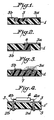
- Conventional circuits of this type include, for example, the substrate shown in Figure 4 of the accompanying drawings.
- Figure 4 is a cross-sectional view of one portion of a printed circuit substrate on which electrical circuits are formed.
- openings 2a,2b are formed at prescribed positions in the printed circuit substrate 1′, and a conductor 3, such as a copper foil, is printed on to the top and bottom surfaces of the printed circuit substrate 1′ and interior surfaces of the holes 2a,2b in accordance with the circuit wiring pattern as shown.
- This conductor 3 is formed by a well known printed wiring technique such as, for example, etching and plating.
- a resistor 4 is connected to the printed circuit substrate 1′ by lead wires 4a,4b which are soldered into the openings 2a,2b. This resistor 4 forms a part of one of the electrical circuits.
- electrical circuits are formed by attaching circuit elements such as the resistor 4 to the surface of the printed circuit substrate 1′ after the aforementioned conductor 3 has been printed on to the substrate.
- unnecessary irregularities can be created on the surface of the printed circuit board.
- the printed circuit substrate 1′ will be damaged by the heat generated by the soldering of the lead wires.
- soldering is insufficient, unsatisfactory electrical connections may result.
- the present invention was conceived in light of the abovementioned problems encountered in conventional circuitry.
- a printed circuit comprising conductive material which forms circuit elements embedded within a dielectric substrate.
- the conductive material may be a low-conductivity material which forms a resistor or a high-dielectric constant material which forms a capacitor.
- the conductive material may be a material having high magnet permeability.
- the dielectric substrate preferably is a porous dielectric material, more preferably a continuously porous dielectric material and most preferably porous, expanded polytetrafluoroethylene.
- the conductive material may be electrically conductive or light conducting.
- the conductive material may be impregnated within the dielectric substrate.
- a printed circuit is provided wherein the electrically conductive material which forms the circuit elements is embedded within a dielectric substrate.
- the preferred dielectric substrate is porous, expanded polytetrafluoroethylene.
- printed circuit substrate in the present invention, materials which form circuit elements are contained inside a dielectric substrate.
- the term "printed circuit substrate” is used herein as a general term for substrates used for the printed wiring of electrical circuits and optical circuits, and includes, for example, substrates which are generally referred to as printed wiring boards, printed circuit boards or printed wiring substrates.
- circuits are contained inside the substrate, no unnecessary irregularities are created on the surface of the printed circuit substrate. Furthermore, since there is no need to attach circuit elements after assembly, unsatisfactory electrical connections due to faulty soldering are minimized. Moreover, desired circuits can be formed merely by laminating a multiple number of substrates together.
- Figure 1 illustrates one example of the present invention.
- printed circuit substrate 1 contains a low-conductivity material 5, such as polytetrafluoroethylene filled with carbon black, that forms a resistor in an electrical circuit.
- This material 5 is contained so that it is partially exposed at the surface of the substrate 1.
- Conductors 3a,3b, consisting of copper foil, are printed on the surface of the printed cirucit substrate 1 so that the conductors separately contact the aforementioned low-conductivity material 5.
- These conductors 3a,3b are printed by a well known wiring technique such as etching or plating in the same manner as in the abovementioned conventional technology.
- the dielectric which makes up the printed circuit substrate 1 is preferably formed from expanded, porous polytetrafluoroethylene, which is continuously porous material, and the printed circuit substrate 1 can be impregnated with the low-conductivity material 5, so that this material is contained inside the pores of the substrate. Furthermore, the impregnation of the substrate with the abovementioned low-conductivity material 5 can be promoted by pre-impregnating the target region, where the low-conductivity material 5 is to be installed, with a solvent used for substitution purposes. The low-conductivity material 5 thereby forms a resistor, and the conductors 3a,3b form lead wires, thereby completing one portion of an electrical circuit according to the invention.
- FIG. 2 illustrates a second example of the present invention.
- a high-dielectric constant material 6 such as polytetrafluoroethylene tape filled with TiO2 or BaTiO3 powder, which forms a capacitor, is contained in the printed circuit substrate 1 so that said material 6 is exposed at the top and bottom surfaces of the printed circuit substrate 1.
- Conductors 3a,3b are printed by the same method as in the aforementioned first example, so that these conductors separately contact the top and bottom surfaces of the high-dielectric constant material 6.
- the structure and effects are substantially the same as in the aforementioned first example.
- Figure 3 illustrates a third example of the present invention.
- a high-magnetic-permeable material 7 such as polytetrafluoroethylene tape filled with molybdenum permalloy powder, is contained inside the printed circuit substrate 1, and conductors 3a, 3b are wired parallel to each other on the surface of the printed circuit substrate 1.
- the material used to form the printed circuit substrate was expanded, porous polytetrafluoroethylene.
- the material used for the substrate is not limited to this material.
- a porous dielectric such as porous polyester could also be used.
- Circuit elements which are attached after assembly as in conventional circuitry can be utilized together with the present invention.
- materials for optical circuits can also be contained inside the printed circuit substrate.
- circuit formation using a single substrate 1 were described above. However, it would also be possible to form circuits on substrates installed above or below the abovementioned substrate of the present invention, or jointly with substrates installed above and/or below the above-mentioned substrate of the present invention.
Landscapes
- Engineering & Computer Science (AREA)
- Microelectronics & Electronic Packaging (AREA)
- Physics & Mathematics (AREA)
- Electromagnetism (AREA)
- Mechanical Engineering (AREA)
- Parts Printed On Printed Circuit Boards (AREA)
- Production Of Multi-Layered Print Wiring Board (AREA)
- Laminated Bodies (AREA)
- Manufacture Of Porous Articles, And Recovery And Treatment Of Waste Products (AREA)
Applications Claiming Priority (2)
| Application Number | Priority Date | Filing Date | Title |
|---|---|---|---|
| JP1987177167U JPH0180974U (de) | 1987-11-20 | 1987-11-20 | |
| JP177167/87U | 1987-11-20 |
Publications (2)
| Publication Number | Publication Date |
|---|---|
| EP0317256A2 true EP0317256A2 (de) | 1989-05-24 |
| EP0317256A3 EP0317256A3 (de) | 1989-09-06 |
Family
ID=16026359
Family Applications (1)
| Application Number | Title | Priority Date | Filing Date |
|---|---|---|---|
| EP88310759A Withdrawn EP0317256A3 (de) | 1987-11-20 | 1988-11-15 | Ein Substrat für gedruckte Schaltungen |
Country Status (5)
| Country | Link |
|---|---|
| US (1) | US4895756A (de) |
| EP (1) | EP0317256A3 (de) |
| JP (1) | JPH0180974U (de) |
| AU (1) | AU2177288A (de) |
| GB (1) | GB2212669A (de) |
Cited By (7)
| Publication number | Priority date | Publication date | Assignee | Title |
|---|---|---|---|---|
| WO2000002209A1 (es) * | 1998-07-06 | 2000-01-13 | Aragonesa De Componentes Pasivos, S.A. | Pista resistiva alta temperatura |
| WO2001001453A3 (en) * | 1999-06-29 | 2001-07-26 | Sun Microsystems Inc | Method and apparatus for adjusting electrical characteristics of signal traces in layered circuit boards |
| EP1265468A3 (de) * | 2001-06-05 | 2005-01-19 | Kabushiki Kaisha Toshiba | Verfahren zur Herstellung eines Verbundbauteils |
| US6906423B1 (en) | 2001-06-05 | 2005-06-14 | Kabushiki Kaisha Toshiba | Mask used for exposing a porous substrate |
| WO2019216885A1 (en) * | 2018-05-08 | 2019-11-14 | W.L. Gore & Associates, Inc. | Flexible and stretchable printed circuits on stretchable substrates |
| WO2019216883A1 (en) * | 2018-05-08 | 2019-11-14 | W.L. Gore & Associates, Inc. | Flexible printed circuits for dermal applications |
| US11330711B2 (en) | 2018-05-08 | 2022-05-10 | W. L. Gore & Associates, Inc. | Flexible and durable printed circuits on stretchable and non-stretchable substrates |
Families Citing this family (12)
| Publication number | Priority date | Publication date | Assignee | Title |
|---|---|---|---|---|
| US5506049C1 (en) * | 1991-05-24 | 2001-05-29 | World Properties Inc | Particulate filled composite film and method of making same |
| US5374453A (en) * | 1991-05-24 | 1994-12-20 | Rogers Corporation | Particulate filled composite film and method of making same |
| US5312576B1 (en) * | 1991-05-24 | 2000-04-18 | World Properties Inc | Method for making particulate filled composite film |
| JP2601128B2 (ja) * | 1992-05-06 | 1997-04-16 | 松下電器産業株式会社 | 回路形成用基板の製造方法および回路形成用基板 |
| US5354603A (en) * | 1993-01-15 | 1994-10-11 | Minnesota Mining And Manufacturing Company | Antifouling/anticorrosive composite marine structure |
| SG93210A1 (en) | 1999-06-29 | 2002-12-17 | Univ Singapore | Method for lamination of fluoropolymer to metal and printed circuit board (pcb) substrate |
| JP2003124538A (ja) * | 2001-10-16 | 2003-04-25 | Sony Corp | 情報記憶装置およびその情報記憶装置を実装した電子機器 |
| GB0703172D0 (en) | 2007-02-19 | 2007-03-28 | Pa Knowledge Ltd | Printed circuit boards |
| KR101591619B1 (ko) | 2008-08-18 | 2016-02-04 | 셈블란트 리미티드 | 할로-하이드로카본 폴리머 코팅 |
| US8995146B2 (en) | 2010-02-23 | 2015-03-31 | Semblant Limited | Electrical assembly and method |
| GB201621177D0 (en) | 2016-12-13 | 2017-01-25 | Semblant Ltd | Protective coating |
| CN110831342A (zh) * | 2019-11-15 | 2020-02-21 | 上海摩软通讯技术有限公司 | 一种miniLED背光模组制备方法 |
Family Cites Families (19)
| Publication number | Priority date | Publication date | Assignee | Title |
|---|---|---|---|---|
| US2866764A (en) * | 1954-03-05 | 1958-12-30 | Minnesota Mining & Mfg | Ink for printing electrical circuits, process for printing a polymer surface therewith, and resulting article |
| FR1117524A (fr) * | 1954-12-14 | 1956-05-23 | Perfectionnements apportés aux appareillages électriques | |
| US3107197A (en) * | 1956-04-18 | 1963-10-15 | Int Resistance Co | Method of bonding a metal to a plastic and the article produced thereby |
| GB923842A (en) * | 1959-09-21 | 1963-04-18 | Morganite Resistors Ltd | Resistive elements |
| GB1156606A (en) * | 1966-05-23 | 1969-07-02 | Dow Chemical Co | Improved Flexible Printed Circuit and Method for the Preparation Thereof |
| US3500428A (en) * | 1967-08-30 | 1970-03-10 | Gen Electric | Microwave hybrid microelectronic circuit module |
| GB1221914A (en) * | 1969-06-13 | 1971-02-10 | Standard Telephones Cables Ltd | Manufacture of integrated circuits |
| GB1266632A (de) * | 1969-06-18 | 1972-03-15 | ||
| IT964199B (it) * | 1971-09-02 | 1974-01-21 | Itt | Sistema di bobine per micromotori di apparecchiature di misura del tempo |
| JPS5348160A (en) * | 1976-10-13 | 1978-05-01 | Hitachi Ltd | Bolt looseness preventing device |
| JPS5469768A (en) * | 1977-11-14 | 1979-06-05 | Nitto Electric Ind Co | Printing circuit substrate with resistance |
| SU864605A1 (ru) * | 1979-06-28 | 1981-09-15 | Предприятие П/Я В-2438 | Способ изготовлени прессзаготовки дл печатных плат |
| US4429216A (en) * | 1979-12-11 | 1984-01-31 | Raychem Corporation | Conductive element |
| GB2096401B (en) * | 1981-04-04 | 1984-10-31 | Int Computers Ltd | Improvements in or relating to electrooptical systems |
| GB2124037B (en) * | 1982-07-19 | 1986-02-26 | Gen Electric Co Plc | Methods of forming patterns on substrates |
| EP0110285A3 (de) * | 1982-11-27 | 1985-11-21 | Prutec Limited | Verbindung integrierter Schaltungen |
| CA1276758C (en) * | 1986-06-02 | 1990-11-27 | Kosuke Moriya | Process for making substrates for printed circuit boards |
| JPH07105577B2 (ja) * | 1986-06-02 | 1995-11-13 | ジヤパンゴアテツクス株式会社 | プリント配線基板の製造法 |
| US4822638A (en) * | 1987-02-11 | 1989-04-18 | Lockheed Corporation | Electronic device fabrication on non-conductive polymer substrate |
-
1987
- 1987-11-20 JP JP1987177167U patent/JPH0180974U/ja active Pending
-
1988
- 1988-09-01 AU AU21772/88A patent/AU2177288A/en not_active Abandoned
- 1988-09-23 US US07/248,158 patent/US4895756A/en not_active Expired - Fee Related
- 1988-11-15 EP EP88310759A patent/EP0317256A3/de not_active Withdrawn
- 1988-11-15 GB GB8826679A patent/GB2212669A/en not_active Withdrawn
Cited By (13)
| Publication number | Priority date | Publication date | Assignee | Title |
|---|---|---|---|---|
| WO2000002209A1 (es) * | 1998-07-06 | 2000-01-13 | Aragonesa De Componentes Pasivos, S.A. | Pista resistiva alta temperatura |
| ES2150859A1 (es) * | 1998-07-06 | 2000-12-01 | Aragonesa Comp | Pista resistiva alta temperatura. |
| WO2001001453A3 (en) * | 1999-06-29 | 2001-07-26 | Sun Microsystems Inc | Method and apparatus for adjusting electrical characteristics of signal traces in layered circuit boards |
| EP1265468A3 (de) * | 2001-06-05 | 2005-01-19 | Kabushiki Kaisha Toshiba | Verfahren zur Herstellung eines Verbundbauteils |
| US6906423B1 (en) | 2001-06-05 | 2005-06-14 | Kabushiki Kaisha Toshiba | Mask used for exposing a porous substrate |
| WO2019216885A1 (en) * | 2018-05-08 | 2019-11-14 | W.L. Gore & Associates, Inc. | Flexible and stretchable printed circuits on stretchable substrates |
| WO2019216883A1 (en) * | 2018-05-08 | 2019-11-14 | W.L. Gore & Associates, Inc. | Flexible printed circuits for dermal applications |
| CN112088582A (zh) * | 2018-05-08 | 2020-12-15 | W.L.戈尔及同仁股份有限公司 | 可拉伸基材上的柔性且可拉伸印刷电路 |
| CN112136367A (zh) * | 2018-05-08 | 2020-12-25 | W.L.戈尔及同仁股份有限公司 | 用于皮肤应用的柔性印刷电路 |
| US11212916B2 (en) | 2018-05-08 | 2021-12-28 | W. L. Gore & Associates, Inc. | Flexible printed circuits for dermal applications |
| AU2018422666B2 (en) * | 2018-05-08 | 2022-03-10 | W. L. Gore & Associates, Inc. | Flexible and stretchable printed circuits on stretchable substrates |
| US11330711B2 (en) | 2018-05-08 | 2022-05-10 | W. L. Gore & Associates, Inc. | Flexible and durable printed circuits on stretchable and non-stretchable substrates |
| US11412609B2 (en) | 2018-05-08 | 2022-08-09 | W. L. Gore & Associates, Inc. | Flexible and stretchable printed circuits on stretchable substrates |
Also Published As
| Publication number | Publication date |
|---|---|
| AU2177288A (en) | 1989-05-25 |
| JPH0180974U (de) | 1989-05-30 |
| GB8826679D0 (en) | 1988-11-15 |
| US4895756A (en) | 1990-01-23 |
| EP0317256A3 (de) | 1989-09-06 |
| GB2212669A (en) | 1989-07-26 |
Similar Documents
| Publication | Publication Date | Title |
|---|---|---|
| EP0317256A2 (de) | Ein Substrat für gedruckte Schaltungen | |
| EP0379686B1 (de) | Gedruckte Schaltungsplatte | |
| US7188410B2 (en) | Insertion of electrical component within a via of a printed circuit board | |
| US7155815B2 (en) | Electrical contacting method | |
| US3701838A (en) | Circuit board | |
| US7569773B2 (en) | Wired circuit board | |
| US5671123A (en) | IC card with a discharge pattern and a ground pattern separated from each other | |
| JPH06131919A (ja) | フレキシブル配線ケーブル | |
| US3693052A (en) | Electrical component mounting | |
| JP2515948B2 (ja) | 宇宙飛行電子技術用のllccc素子の電気接続方法 | |
| JPH03183106A (ja) | プリント配線板 | |
| US5083237A (en) | Electronic parts and electronic device incorporating the same | |
| US4357647A (en) | Printed circiuit board | |
| JP2757748B2 (ja) | プリント配線板 | |
| JP2789406B2 (ja) | 回路基板 | |
| JP2001135920A (ja) | 樹脂成形回路基板及びその製造方法 | |
| JPH10163004A (ja) | 抵抗器、コンデンサ、インダクタ及びコネクタ | |
| JPS6384190A (ja) | チツプ部品搭載基板 | |
| JPH1154854A (ja) | プリント配線板 | |
| US4762732A (en) | Process for forming silver conductors on a substrate | |
| JPH01216591A (ja) | プリント基板 | |
| JPH01789A (ja) | 超電導配線プリント板 | |
| JPH02102594A (ja) | 混成集積回路基板 | |
| KR100507625B1 (ko) | 크림 솔더를 이용한 표면실장형 전기장치 및 그 제조방법 | |
| JPH11177205A (ja) | プリント配線板 |
Legal Events
| Date | Code | Title | Description |
|---|---|---|---|
| PUAI | Public reference made under article 153(3) epc to a published international application that has entered the european phase |
Free format text: ORIGINAL CODE: 0009012 |
|
| AK | Designated contracting states |
Kind code of ref document: A2 Designated state(s): AT BE CH DE ES FR GB GR IT LI LU NL SE |
|
| PUAL | Search report despatched |
Free format text: ORIGINAL CODE: 0009013 |
|
| AK | Designated contracting states |
Kind code of ref document: A3 Designated state(s): AT BE CH DE ES FR GB GR IT LI LU NL SE |
|
| 17P | Request for examination filed |
Effective date: 19900209 |
|
| STAA | Information on the status of an ep patent application or granted ep patent |
Free format text: STATUS: THE APPLICATION HAS BEEN WITHDRAWN |
|
| 18W | Application withdrawn |
Withdrawal date: 19900919 |
|
| R18W | Application withdrawn (corrected) |
Effective date: 19900919 |