EP0317414B1 - Flache Antenne mit SSL-Speisenetzwerk, bestehend aus selbsttragenden, mit dicken strahlenden Schlitzen ausgerüsteten Masseflächen ohne Positionierungsstifte - Google Patents
Flache Antenne mit SSL-Speisenetzwerk, bestehend aus selbsttragenden, mit dicken strahlenden Schlitzen ausgerüsteten Masseflächen ohne Positionierungsstifte Download PDFInfo
- Publication number
- EP0317414B1 EP0317414B1 EP88402848A EP88402848A EP0317414B1 EP 0317414 B1 EP0317414 B1 EP 0317414B1 EP 88402848 A EP88402848 A EP 88402848A EP 88402848 A EP88402848 A EP 88402848A EP 0317414 B1 EP0317414 B1 EP 0317414B1
- Authority
- EP
- European Patent Office
- Prior art keywords
- antenna element
- slots
- element according
- dielectric
- antenna
- Prior art date
- Legal status (The legal status is an assumption and is not a legal conclusion. Google has not performed a legal analysis and makes no representation as to the accuracy of the status listed.)
- Expired - Lifetime
Links
- 229910052751 metal Inorganic materials 0.000 claims description 38
- 239000004020 conductor Substances 0.000 claims description 37
- 239000002184 metal Substances 0.000 claims description 37
- 230000005284 excitation Effects 0.000 claims description 19
- 239000006260 foam Substances 0.000 claims description 6
- 238000005520 cutting process Methods 0.000 claims description 5
- 230000002093 peripheral effect Effects 0.000 claims 1
- 238000004519 manufacturing process Methods 0.000 description 16
- 230000010287 polarization Effects 0.000 description 11
- 238000007493 shaping process Methods 0.000 description 11
- 230000008901 benefit Effects 0.000 description 7
- 238000013461 design Methods 0.000 description 6
- 238000000034 method Methods 0.000 description 5
- 238000004364 calculation method Methods 0.000 description 4
- 239000003989 dielectric material Substances 0.000 description 4
- 238000005259 measurement Methods 0.000 description 4
- 230000003071 parasitic effect Effects 0.000 description 4
- 230000006978 adaptation Effects 0.000 description 3
- 238000004026 adhesive bonding Methods 0.000 description 3
- 239000000758 substrate Substances 0.000 description 3
- 239000011248 coating agent Substances 0.000 description 2
- 238000000576 coating method Methods 0.000 description 2
- 230000008878 coupling Effects 0.000 description 2
- 238000010168 coupling process Methods 0.000 description 2
- 238000005859 coupling reaction Methods 0.000 description 2
- 238000005553 drilling Methods 0.000 description 2
- 238000003754 machining Methods 0.000 description 2
- 238000012423 maintenance Methods 0.000 description 2
- 238000003466 welding Methods 0.000 description 2
- 230000005540 biological transmission Effects 0.000 description 1
- 230000015572 biosynthetic process Effects 0.000 description 1
- 230000005465 channeling Effects 0.000 description 1
- 230000000295 complement effect Effects 0.000 description 1
- 238000010276 construction Methods 0.000 description 1
- 238000011161 development Methods 0.000 description 1
- 238000009826 distribution Methods 0.000 description 1
- 230000000694 effects Effects 0.000 description 1
- 230000005684 electric field Effects 0.000 description 1
- 238000005516 engineering process Methods 0.000 description 1
- 239000003292 glue Substances 0.000 description 1
- 238000007654 immersion Methods 0.000 description 1
- 230000006872 improvement Effects 0.000 description 1
- 238000003780 insertion Methods 0.000 description 1
- 230000037431 insertion Effects 0.000 description 1
- 239000010410 layer Substances 0.000 description 1
- 239000000463 material Substances 0.000 description 1
- 239000007769 metal material Substances 0.000 description 1
- 239000002991 molded plastic Substances 0.000 description 1
- 239000004223 monosodium glutamate Substances 0.000 description 1
- 230000007935 neutral effect Effects 0.000 description 1
- 230000035515 penetration Effects 0.000 description 1
- 229920002635 polyurethane Polymers 0.000 description 1
- 239000004814 polyurethane Substances 0.000 description 1
- 230000008569 process Effects 0.000 description 1
- 239000011241 protective layer Substances 0.000 description 1
- 230000005855 radiation Effects 0.000 description 1
- 238000011084 recovery Methods 0.000 description 1
- 230000009467 reduction Effects 0.000 description 1
- 239000005871 repellent Substances 0.000 description 1
- 230000002940 repellent Effects 0.000 description 1
- 238000007650 screen-printing Methods 0.000 description 1
- 239000007787 solid Substances 0.000 description 1
- 125000006850 spacer group Chemical group 0.000 description 1
- 230000009897 systematic effect Effects 0.000 description 1
- 238000012549 training Methods 0.000 description 1
Images




Classifications
-
- H—ELECTRICITY
- H01—ELECTRIC ELEMENTS
- H01Q—ANTENNAS, i.e. RADIO AERIALS
- H01Q21/00—Antenna arrays or systems
- H01Q21/24—Combinations of antenna units polarised in different directions for transmitting or receiving circularly and elliptically polarised waves or waves linearly polarised in any direction
-
- H—ELECTRICITY
- H01—ELECTRIC ELEMENTS
- H01Q—ANTENNAS, i.e. RADIO AERIALS
- H01Q21/00—Antenna arrays or systems
- H01Q21/0006—Particular feeding systems
- H01Q21/0075—Stripline fed arrays
- H01Q21/0081—Stripline fed arrays using suspended striplines
-
- H—ELECTRICITY
- H01—ELECTRIC ELEMENTS
- H01Q—ANTENNAS, i.e. RADIO AERIALS
- H01Q21/00—Antenna arrays or systems
- H01Q21/06—Arrays of individually energised antenna units similarly polarised and spaced apart
- H01Q21/061—Two dimensional planar arrays
- H01Q21/064—Two dimensional planar arrays using horn or slot aerials
Definitions
- EP-A-0 252 779 belongs to the state of the art as defined in Article 54 (3) (EPC).
- planar antennas of the type of array antennas capable of being used for this purpose are designed on criteria of maximum efficiency, using sophisticated embodiments which are hardly compatible with mass production at cost. reduced.
- patent EP-A-0 123 350 describes a microstrip suspended by positioning pads between two metal plates. These metal plates are machined so as to form waveguides coupled to terminations of the central conductor.
- the embodiments described in this prior patent always involve a machining operation in a very thick metal plate (of the order of 7 to 10 mm, at 12 GHz).
- planar antenna with external waveguides described in the European patent application of 16/12/86, (RTC-COMPELEC) designating the FRG, France, and Great Britain, and published under the n ° EP-A1-0228 742.
- the antenna described comprises flexible sheets forming supports for manufacturing screen-printed studs interposed between the supply circuit and the external waveguides.
- This embodiment is obviously still very expensive, because of the need to manufacture the waveguides, and to use separate support sheets, further undergoing a screen printing treatment for the formation of associated pads.
- the planar microwave antenna of the main patent and certificate of addition applications mentioned in the preamble advantageously resolves the above drawbacks, by providing for the use of self-supporting ground planes pierced with radiating slots, in which are repelled by stamping, positioning pads.
- the repositioned positioning pads are intended to come to rest on non-conductive portions of the suspended substrate.
- the drilling of the slots on the one hand, and the pushing back of the positioning pads on the other hand would imply the use of a more complex stamping tool, or even of two separate tools.
- Another object of the invention is more generally to produce a network antenna of simple construction, with low tolerance requirements, compatible with a mass production process, at low cost price.
- Another object of the invention is to provide a planar antenna with radiating slits, and not with waveguides, so as to overcome the problems of thickness of the machining plates and tolerance.
- An additional objective of the invention is to maintain the spacing between the circuit supply and ground planes, no longer by means of specific studs, but on the contrary, essentially, by the very structure of the radiating slots, which makes it possible to keep the conductor at the level of the excitation terminations, c that is to say at the most critical location of the radiating slot antenna. This also makes it possible to multiply the density of the holding points of the supply circuit.
- An additional objective of the invention is to conform the ground plans according to an economic shaping process.
- the shaping of the ground planes consists simply in carrying out a double operation, combined or not, of cutting / stamping of the slots.
- this shaping is perfectly identical for the upper and lower metal plates forming ground planes.
- An additional objective or advantage of the invention is to avoid the untimely propagation, if necessary, of parasitic modes of radiation between the plates of the antenna.
- an antenna element of the type comprising a central microstrip conductor and at least one ground plane, said central conductor cooperating with radiating slots formed in the ground plane, said central conductor being a microstrip conductor carried by a dielectric support sheet suspended on said ground plane, which is a thin self-supporting metallic plate forming a thin structure with said dielectric support sheet, characterized in that at least some said radiating slots are slot-slots each having a substantially vertical wall on at least part of the periphery of the slot, said wall or wall portion acting as a stud positioning maintaining the spacing between said central conductor and said ground plane.
- the dielectric support sheet is suspended between two self-supporting thin metal plates forming upper and lower ground planes.
- Said substantially vertical walls of the thick slots are advantageously formed by pushing back the thin metal plates forming ground planes.
- a single stamping operation could carry out both the drilling of the slot, and the pushing back of the walls or spacing wall portions.
- the walls or wall portions of thick slots are added by gluing, welding, force fitting or the like.
- each slot-stud can be produced according to several variants, as regards its shape (circular, rectangular, etc.), the arrangement of the walls or portions of walls (interrupted, symmetrical portions. ..), and the shape of the walls (rounded edges in contact with the dielectric support of the central conductor).
- each vertical wall must be interrupted at the level of the passage of the conductive termination of excitation of the radiating slot.
- the slot-studs have walls allowing the passage of two excitation terminations, for operation in circular polarization (s), or even in linear polarization.
- FIG. 1 represents an embodiment of the invention comprising a thin dielectric support sheet 12 carrying a microstrip conductor 22 and suspended between two thin self-supporting metal plates 11, 13, respectively forming upper and lower ground planes.
- the structure 11, 12, 13 thus formed has pairs of radiating slots 20a, 20b, superimposed at an excitation termination 30 of the conductor 22.
- Each pair of slots 20a, 20b and the excitation termination 30 of the conductor 22 associated form a radiating element of the antenna.
- each of the slots 20a, 20b comprises a substantially vertical wall 31a, 31b.
- the vertical wall is integral with the metal plates 11, 13, and constitutes the folded edges of the slots 20a, 20b, shaped for example following a stamping operation.
- the total thickness of the slot-plot thus formed depends on the distance from the ground planes 11, 13, which is mainly defined by the characteristic impedance of the supply line.
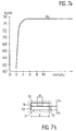
- This impedance is mainly defined by the ratio w / b, w representing the width of the printed conductor, and b the distance between the ground planes 11, 13 (fig. 2).
- the ratio w / b is substantially equal to 1, for impedances of the supply line 11, 12, 13 of the order of 60 Ohm which interests us.
- w must be sufficiently small, preferably less than 2 mm in the case of a 12 GHz antenna, so that the supply lines 22 can pass between the slots without being too close to the slots, or one on the other, to avoid parasitic couplings, it can be seen that the total thickness of the stud slots 20a, 20b must be less than approximately 2 mm, that is to say less than 0.1 times the wavelength approximately ("Stripline circuit design" H.HOWE Jr, Artech House, 1974).
- the wall 31a of the upper slot 20a has a notch or interruption 32 clearing a passage for the excitation termination 30.
- the dimensions of the passage must be sufficient to neutralize any parasitic influence of the vertical wall 31a on the termination 30, as is the case. will see below.
- a similar interruption is also provided in the vertical wall 31b.
- the vertical walls 31a, 31b of the radiating slots which ensure the relative positioning and spacing of the ground planes 11, 13 relative to the central dielectric 12, and therefore to the excitation conductor 22, 30.
- each of the metal plates 11, 13 essentially boils down, for example, to a stamping operation of the slots, followed or preceded by a cutting or other operation intended to flatten the contact edge of the walls. 31a, 31b, and to clear the interruption 32 of passage of the excitation termination 30 of the driver. Because the slots-pads thus produced ensure the maintenance and spacing of the ground planes, it is therefore not necessary in the general case to provide additional spacing pads. In addition, the fact that the spacing walls of the plates 11, 13 are located at the excitation terminations of the radiating slots guarantees that nominal spacing is maintained at the most critical points.
- This embodiment also allows the use of self-supporting metal plates 11, 13 of very small thickness, due to the fact that the rigidity of each metal plate 11, 13 is reinforced by the multiplicity of repelled walls 31a, 31b, and the multiplicity of support points along the contact edges of the walls 31a, 31b .
- pairs of radiating slots 20a, 20b has the effect of concentrating the radiant energy in a zone smaller than that of the embodiments where each conductive termination is only coupled to cavities forming waveguides, in particular that the width of a waveguide is greater than the width D e of the corresponding radiating slots, for a given working frequency.
- the measurements carried out on prototype have shown that the slot operates from 10 GHz, with a T.O.S. less than 1.4. This is to be compared with the cut-off frequency of a circular guide of the same diameter (16.5 mm) is equal to 10.65 GHz. Such a guide would therefore only function correctly beyond 10.65 GHz, and therefore outside the working range of the radiating slot-studs of the present invention.
- slot-studs of the invention does not exclude that it is optionally possible to provide the radiating elements with open front cavities 27 and / or closed rear 26, as shown in FIG. 2.
- the suspended lines of the invention make it possible to substantially reduce the losses likely to occur between the central conductor and the ground planes, due to the use of air as a dielectric, unlike the equivalent “stripline” or “microstrip” type antennas using a solid and expensive dielectric material.
- FIGS 2 and 3 relate to embodiments of the antenna according to the invention in the form of modules of several radiating elements.
- Each module thus advantageously comprises a network of radiating elements, regularly arranged in rows and columns.
- FIGS. 2 and 3 correspond to vertical sections of modules, along an axis of alignment of radiating elements, but it can be imagined that the module has a plurality of alignments of identical elements in other planes parallel to the cutting plane.
- the spacing between two consecutive radiating elements on a row or a column can be equal to 0.7 to 0.9 wavelength.
- each thin self-supporting metal plate 11, 13 thus undergoes a cutting / stamping operation as defined above. simultaneously forming a plurality of slot-studs.
- the dielectric support 12 of the excitation conducting line 22 comprises a plurality of excitation terminations 30 arranged opposite the pairs of slot-studs corresponding to each radiating element. This design is particularly suitable for a mass production method of antennas.
- an antenna can be produced by combining several modules.
- this technique has the advantage of reducing the manufacturing cost, by reducing the size of the tools used.
- the savings made can be significant; moreover, the reduction in the size of the tools makes it possible to better control the precision of setting in the form of stamped plates.
- the advantage is even more decisive if each antenna is made by adding several identical modules.
- connection means between modules can be produced by input / output waveguides, or by connection of input / output terminations of adjacent modules (see fig. 19, 20, 21 of European patent application EP-A-0 252 779).
- the structure 11, 12, 13 is completed by a stamped bottom plate 14 forming closed cavities 26, and by a stamped upper crown 25 forming open cavities 27.
- the embodiment shown comprises a cavity per radiating element.
- cavities in particular closed rear cavities, common to several radiating elements, for example four adjacent radiating elements in "square".
- the antenna module with a simple flat bottom plate devoid of cavities.
- this embodiment of the antenna exclusively involves a metal sheet stamping technology for the manufacture of the four plates 11, 13, 14, 25.
- the stamping operation makes it possible on the one hand to form the slot-studs 20a, 31a; 20b, 31b, and on the other hand, to form the crown 25 with open cavities 27, and the stamped bottom plate 14 with closed cavities 26.
- the shaping of the upper crown 25 is very similar to the shaping of the slot-studs of the present invention, and that the shaping of the closed cavities 26 in the bottom plate 14 can be analogous to the method of shaping the bulges or stops forming positioning pads in the embodiments of European application EP-A-0 252 779.
- Figure 2 does not in any way account for the proportion of spacings and thicknesses of the plates, which have been considerably deformed for reasons of clarity.
- the bottom reflecting plate 14 makes it possible to give a direction to the radiated energy, and is located at a distance from the structure of the order of 1/4 of the wavelength in the rear cavity. This distance is a parameter for adjusting the operation of the antenna together with the dimensions of the supply line 22 and the dimensions of the slot-studs.
- the shape of the bottom plate 14 to present closed rear cavities 26, and the possible addition of open front cavities 27, makes it possible to further optimize the recovery and the channeling in the direction of transmission / reception of the antenna. of most of the radiated energy.
- open front cavities 27 increases the gain of the antenna.
- the height of the cavities is preferably greater than 0.1 times the emission wavelength.
- a height of the open cavities 27 of 5 mm to 10 mm would give an increase in gain of the order of 2 dB, depending on the geometry, for an operating frequency of 12 GHz.
- the plates 14, 13, 12, 11 and 25 can be assembled by simple stacking, with fastening by bolting, or by insertion into a box B with cover C, as shown in FIG. 3.
- cavities 26, 27 can also be produced in the form of stamped individual cabochons, by metal rings, by sets of interlocking blades placed on the field, or even by metal coating applied to a preformed non-metallic material, as described in the above-mentioned earlier patent applications.
- slot-studs 20a, 31a; 20b, 31b can also be carried out by attaching metal rings, or criss-cross blades placed on the field, on the self-supporting thin metal plates 11, 13, as described below with reference to FIG. 9.
- the antenna module shown comprises alignments of 5 radiating elements.
- Figure 3 is a vertical sectional view along one of these alignments.
- the module is provided with a polarizer P.
- Circular polarization can be obtained by using a printed plane polarizer (for example a meandering line polarizer) placed above the radiating elements.
- a printed plane polarizer for example a meandering line polarizer
- Another method of obtaining a circular polarization consists in exciting two perpendicular linear polarizations, phase shifted by ⁇ 90 ° in each of the radiating elements, as shown in FIG. 10.
- Figures 4 and 5 are top views illustrating preferred embodiments of the conformation of the slot-studs according to the invention.
- the width l of the interrupt 32 must be greater than 4 to 5 mm, for a slit diameter approximately equal to 15.5 mm.
- the conductor 22 of the line has been placed in the conditions of the slot-stud antenna, that is to say between two upper horizontal walls 70 and lower 71 respectively, representing the ground planes, and between two vertical walls 72, 73 representing the substantially vertical walls of the slot-studs.
- the conductor 22 is mounted on a dielectric support 74.
- the walls 70, 71, 72, 73 are made of conductive material.
- the value of the impedance Z0 is a crucial parameter determining the performance of the antenna and the adaptation of each radiating element.
- the curve Z0 f (A) in FIG. 7a, clearly indicates that the impedance Z0 stabilizes beyond a value of 4 to 5 mm for the variable A. Consequently, provided that this minimum spacing is respected, the antenna performance is stable and perfectly controlled.
- the T.O.S. was less than about 1.4 between 10 and 11.5 GHz, or a bandwidth of 1.5 GHz, for a diameter of the slot-plot of 16.5 mm.
- the slot-studs consist of two portions of substantially vertical walls 51, 52; 61, 62. These wall portions are placed symmetrically with respect to the axis of penetration of the excitation terminations 30 between the pairs of slots.
- the substantially vertical walls of the slot-studs consist of a plurality of small portions distributed regularly or not over the periphery of the slots.
- the wall portion can be limited to a single element a few millimeters in width, for example, or even possibly to no element for some of the slots if the maintenance the spacing of the structure is sufficiently ensured at the level of adjacent slots.
- the slot-studs of the invention may, in certain variants, have the characteristics shown diagrammatically in FIGS. 8 and 9.
- the substantially vertical walls 31a, 31b have a rounded support edge 81a, 81b, to better support the dielectric 12.
- the diameters of the slot at the level of the dielectric 12, and at the level of the planes of mass 11, 13 are not equal, and must therefore be optimized for the operating frequency.
- each ring 90 or ring portions 91 determines, by its thickness, the spacing of the structure.
- rings or portions of rings 90, 91 can be added by gluing, welding, press fitting, or the like.
- the present invention also includes the case where only some of the radiating slots are slot-studs, and / or the case where additional studs spacers, formed by pushing back into the ground planes 11, 13, or else formed by metallic or non-metallic elements attached to the ground planes, are inserted into the structure. It is also possible to provide for filling the structure with a dielectric material, for example in the form of foam, to increase its rigidity.
- the antenna modules according to the invention can also be coated with an electromagnetically neutral material of the type of an expanded or molded plastic, for example expanded polyurethane.
- This coating has the particular advantage of protecting the module against bad weather when the antenna is to be used outside.
- the slot-in embodiment is also compatible with multi-level antennas of the type presented in FIG. 6 of European application EP-A-0 252 779, or also with the embodiments with additional coupling elements ( Fig. 7 of the same European application).
- the various superimposed plates constituting the antenna according to the invention can be joined together, for example by gluing, during a manufacturing process comprising a step of immersion of the bearing edges of the plates in a glue bath, before application of each plate on the previous plate.
- FIGS. 11 to 14 illustrate embodiments of the invention in which the antenna element comprises only a single ground metal plate, the upper plate 11 or the lower plate 13.
- the antenna element corresponds to that shown in Figure 2 without the upper plate 11 and without the upper ring 25.
- the printed conductors 30 have been shown on the upper part of the dielectric plate 12; we can also design an antenna element of the same type but in which these printed conductors 30 will be arranged on the underside of the plate 12.
- the printed circuit plate 12 can constitute a protective layer or radome; this layer can also be made of expanded foam since the thickness of the dielectric 12 is no longer involved in the calculations.
- Figure 12 shows an alternative embodiment of Figure 3 in which the upper metal plate has been removed.
- FIG. 13 corresponds to that of FIG. 2 in which the lower metal ground plate 13 has been removed.
- the printed conductors 30 must not touch the cavities, the minimum allowable distance being of the order of 0.5 mm for typical antenna dimensions operating at 12 GHz.
- this plate may include positioning push-backs, with or without a vertical wall of radiating slots, to maintain the dielectric plate 12.
- FIG. 14 represents an embodiment which comprises only a single upper metal plate 11, the vertical walls being constituted by crowns or crown portions formed by repellents 104 produced in a dielectric or a dielectric foam 103 on which the circuit rests thin print 12.
- this dielectric or dielectric foam 103 may include rear cavities.
- FIG. 15 represents an alternative embodiment comprising two independent printed circuit boards 12a and 12b which are intended to create two circular or linear polarizations independent.
- certain slots of the metal plate 105, separating the circuits 12a, 12b have vertical walls directed upwards and others downwards.
- the calculation of the feed lines must be redone as regards the impedance; it is especially the width of the printed conductors which must be recalculated.
Landscapes
- Waveguide Aerials (AREA)
- Details Of Aerials (AREA)
Claims (15)
- Antennenelement des Typs mit einem zentralen Mikrobandleiter (22) und mindestens einer Massefläche (11,13), wobei der zentrale Leiter (22) mit in der Massefläche (11,13) angeordneten strahlenden Schlitzen (20a,20b) zusammenwirkt, wobei der zentrale Leiter ein Mikrobandleiter ist, der von einem dielektrischen Trägerblatt (12) getragen wird, das über der Massefläche aufgehängt ist, die ein dünnes selbsttragendes Metallplättchen ist, das mit dem dielektrischen Trägerblatt (12) eine dünne Struktur bildet, dadurch gekennzeichnet, daß mindestens einige der strahlenden Schlitze (20a,20b) Schlitzstifte sind, von denen jeder eine im wesentlichen vertikale Wand (31a,31b) über mindestens einem Teil des Schlitzrandes aufweist, wobei die Wand oder der Wandabschnitt (31a,31b;51,52;61,62) die Rolle eines Positionierungsstifts spielt, der den Abstand (Hu ,HL) zwischen dem zentralen Leiter (22) und der Massefläche (11,13) haltet.
- Antennenelement nach Anspruch 1, in dem das dielektrische Trägerblatt (12) zwischen zwei dünnen selbsttragenden Metallplättchen (11,13) aufgehängt ist, die eine obere (11) und untere (13) Massefläche bilden, in denen die Schlitzstifte (20a,20b) paarweise miteinander ausgerichtet angeordnet sind.
- Antennenelement nach Anspruch 1 oder 2, dadurch gekennzeichnet, daß die im wesentlichen vertikalen Wände (31a,31b;51,52,61,62) durch Treiben der Ränder der Schlitze (20a,20b) gebildet werden.
- Antennenelement nach Anspruch 2, dadurch gekennzeichnet, daß die im wesentlichen vertikalen Wände (31a,31b;51,52,61,62) aus Kränzen oder Kranzabschnitten (90,91) gebildet sind, die zwischen den Metallplättchen (11,13) und dem dielektrischen Träger (12) eingesetzt sind.
- Antennenelement nach Anspruch 1 oder 2, dadurch gekennzeichnet, daß die vertikalen Wände (31a,31b) einen Ausschnitt (32) in Höhe der Durchführung des Anregungsendstücks (30) des Leiters (22) aufweisen.
- Antennenelement nach Anspruch 1 oder 2, dadurch gekennzeichnet, daß mindestens einige der strahlenden Schlitze Schlitzstifte sind, die zwei im wesentlichen vertikale Wandabschnitte (51,52,61,62) aufweisen, die symmetrisch bezüglich der Achse verteilt sind, entlang der das Anregungsendstück (30) des Leiters (22) in das Innere des Schlitzpaares (20a,20b) eingeführt ist.
- Antennenelement nach Anspruch 1 oder 2, dadurch gekennzeichnet, daß die im wesentlichen vertikalen Wände (31a,31b;51,52,61,62) einen Stützrand (81a,81b) aufweisen, der im wesentlichen am Kontakt des dielektrischen Trägers (12) abgerundet ist.
- Antennenelement nach Anspruch 1 oder 2, dadurch gekennzeichnet, daß mindestens einige der strahlenden Schlitze (20a,20b) zwei Ausschnitte (32) in den im wesentlichen vertikalen Wänden (31a,31b) aufweisen, um zwei Anregungsendstücke (101,102) im Winkel von 90° durchzuführen.
- Antennenelement nach Anspruch 1 oder 2, dadurch gekennzeichnet, daß mindestens einige der strahlenden Schlitze mit vorderen offenen Hohlräumen (27) und/oder hinteren geschlossenen Hohlräumen (26) zusammenwirken.
- Antennenelement nach Anspruch 3, dadurch gekennzeichnet, daß die Schlitzstifte (20a,20b) im Laufe eines doppelten Arbeitsgangs aus gleichzeitigem oder aufeinanderfolgendem Schneiden und Ziehen mehrerer Schlitzstifte in jedem der selbsttragenden dünnen Plättchen (11,13), die die Masseflächen bilden, gebildet werden.
- Antennenelement nach Anspruch 1, dadurch gekennzeichnet, daß es nur ein unteres Metallplättchen (13) aufweist.
- Antennenelement nach Anspruch 1, dadurch gekennzeichnet, daß es nur ein oberes Metallplättchen (11) aufweist.
- Antennenelement nach Anspruch 11 oder 12, dadurch gekennzeichnet, daß die vertikalen Wände (31a,31b) aus getriebenen Flächen bestehen, die in einen Dielektrikum oder einem dielektrischen Schaum (103) hergestellt sind, auf dem der dünne gedruckte Schaltkreis (12) liegt.
- Antennenelement nach Anspruch 13, dadurch gekennzeichnet, daß das Dielektrikum oder der dielektrische Schaum (103) hintere oder vordere Hohlräume aufweist.
- Antennenelement nach anspruch 2, dadurch gekennzeichnet, daß es zwei unabhängige gedruckte Schaltkreise (12a,12b) aufweist, die zur Erzeugung zweier unabhängiger Zirkular- oder Linearpolarisationen bestimmt sind.
Applications Claiming Priority (2)
| Application Number | Priority Date | Filing Date | Title |
|---|---|---|---|
| FR8715742A FR2623336B2 (fr) | 1986-06-05 | 1987-11-13 | Antenne plane a microruban suspendu, et plans de masse autoporteurs a fentes rayonnantes epaisses, sans plots de positionnement |
| FR8715742 | 1987-11-13 |
Publications (2)
| Publication Number | Publication Date |
|---|---|
| EP0317414A1 EP0317414A1 (de) | 1989-05-24 |
| EP0317414B1 true EP0317414B1 (de) | 1995-04-12 |
Family
ID=9356780
Family Applications (1)
| Application Number | Title | Priority Date | Filing Date |
|---|---|---|---|
| EP88402848A Expired - Lifetime EP0317414B1 (de) | 1987-11-13 | 1988-11-14 | Flache Antenne mit SSL-Speisenetzwerk, bestehend aus selbsttragenden, mit dicken strahlenden Schlitzen ausgerüsteten Masseflächen ohne Positionierungsstifte |
Country Status (3)
| Country | Link |
|---|---|
| EP (1) | EP0317414B1 (de) |
| DE (1) | DE3853573T2 (de) |
| ES (1) | ES2072266T3 (de) |
Families Citing this family (14)
| Publication number | Priority date | Publication date | Assignee | Title |
|---|---|---|---|---|
| GB8904302D0 (en) * | 1989-02-24 | 1989-04-12 | Marconi Co Ltd | Microwave antenna array |
| JPH03151702A (ja) * | 1989-11-08 | 1991-06-27 | Sony Corp | 平面アレイアンテナ |
| EP0445453A1 (de) * | 1990-03-07 | 1991-09-11 | Stc Plc | Antenne |
| DE69105224T2 (de) * | 1990-03-14 | 1995-04-06 | Northern Telecom Ltd | Antenne. |
| JPH06500909A (ja) * | 1991-06-28 | 1994-01-27 | アルカテル・エスパース | リニアアレイアンテナ |
| GB2312791A (en) * | 1996-05-02 | 1997-11-05 | Northern Telecom Ltd | Antenna array assembly |
| US6507320B2 (en) | 2000-04-12 | 2003-01-14 | Raytheon Company | Cross slot antenna |
| US6535088B1 (en) | 2000-04-13 | 2003-03-18 | Raytheon Company | Suspended transmission line and method |
| US6622370B1 (en) | 2000-04-13 | 2003-09-23 | Raytheon Company | Method for fabricating suspended transmission line |
| US6542048B1 (en) | 2000-04-13 | 2003-04-01 | Raytheon Company | Suspended transmission line with embedded signal channeling device |
| US6552635B1 (en) | 2000-04-13 | 2003-04-22 | Raytheon Company | Integrated broadside conductor for suspended transmission line and method |
| US6518844B1 (en) | 2000-04-13 | 2003-02-11 | Raytheon Company | Suspended transmission line with embedded amplifier |
| US6642898B2 (en) | 2001-05-15 | 2003-11-04 | Raytheon Company | Fractal cross slot antenna |
| US6885264B1 (en) | 2003-03-06 | 2005-04-26 | Raytheon Company | Meandered-line bandpass filter |
Citations (1)
| Publication number | Priority date | Publication date | Assignee | Title |
|---|---|---|---|---|
| EP0252779A1 (de) * | 1986-06-05 | 1988-01-13 | Emmanuel Rammos | Antennenelement mit einem Streifen, der zwischen zwei selbsttragenden und mit untereinanderliegenden strahlenden Schlitzen vorgesehenen Grundplatten hängt und Verfahren zur Herstellung desselben |
Family Cites Families (4)
| Publication number | Priority date | Publication date | Assignee | Title |
|---|---|---|---|---|
| US4131894A (en) * | 1977-04-15 | 1978-12-26 | Ball Corporation | High efficiency microstrip antenna structure |
| FR2523376A1 (fr) * | 1982-03-12 | 1983-09-16 | Labo Electronique Physique | Element rayonnant ou recepteur de signaux hyperfrequences a polarisations circulaires gauche et droite et antenne plane comprenant un reseau de tels elements juxtaposes |
| FR2544920B1 (fr) * | 1983-04-22 | 1985-06-14 | Labo Electronique Physique | Antenne plane hyperfrequences a reseau de lignes a substrat completement suspendu |
| FR2592232B1 (fr) * | 1985-12-20 | 1988-02-12 | Radiotechnique Compelec | Antenne plane hyperfrequences a reseau de lignes a substrat suspendu et methode pour en fabriquer un constituant. |
-
1988
- 1988-11-14 EP EP88402848A patent/EP0317414B1/de not_active Expired - Lifetime
- 1988-11-14 DE DE19883853573 patent/DE3853573T2/de not_active Expired - Fee Related
- 1988-11-14 ES ES88402848T patent/ES2072266T3/es not_active Expired - Lifetime
Patent Citations (1)
| Publication number | Priority date | Publication date | Assignee | Title |
|---|---|---|---|---|
| EP0252779A1 (de) * | 1986-06-05 | 1988-01-13 | Emmanuel Rammos | Antennenelement mit einem Streifen, der zwischen zwei selbsttragenden und mit untereinanderliegenden strahlenden Schlitzen vorgesehenen Grundplatten hängt und Verfahren zur Herstellung desselben |
Also Published As
| Publication number | Publication date |
|---|---|
| DE3853573T2 (de) | 1996-01-04 |
| ES2072266T3 (es) | 1995-07-16 |
| EP0317414A1 (de) | 1989-05-24 |
| DE3853573D1 (de) | 1995-05-18 |
Similar Documents
| Publication | Publication Date | Title |
|---|---|---|
| EP0317414B1 (de) | Flache Antenne mit SSL-Speisenetzwerk, bestehend aus selbsttragenden, mit dicken strahlenden Schlitzen ausgerüsteten Masseflächen ohne Positionierungsstifte | |
| EP0252779B1 (de) | Antennenelement mit einem Streifen, der zwischen zwei selbsttragenden und mit untereinanderliegenden strahlenden Schlitzen vorgesehenen Grundplatten hängt und Verfahren zur Herstellung desselben | |
| EP2664030B1 (de) | Gedruckte schlitzrichtantenne und system mit einer gruppe aus bedruckten schlitzrichtantennen | |
| EP0372451B1 (de) | Multifrequenz-Strahlungsvorrichtung | |
| CA2681548C (fr) | Reseau reflecteur et antenne comportant un tel reseau reflecteur | |
| EP0783189A1 (de) | Flache Mikrowellen-Gruppenantenne für die Kommunikation mit geostationären Fernsehsatelliten | |
| EP2795726B1 (de) | Optisch transparente bedruckte antenne und anordnung von optisch transparenten gedruckten antennen | |
| FR2957719A1 (fr) | Antenne reseau reflecteur a compensation de polarisation croisee et procede de realisation d'une telle antenne | |
| FR2706085A1 (fr) | Structure rayonnante multicouches à directivité variable. | |
| FR2582865A1 (fr) | Modules unitaires d'antenne hyperfrequences et antenne hyperfrequences comprenant de tels modules | |
| FR2698212A1 (fr) | Source élémentaire rayonnante pour antenne réseau et sous-ensemble rayonnant comportant de telles sources. | |
| EP0239069B1 (de) | Streifenleitungsantennengruppe | |
| EP3788674B1 (de) | Breitbanddrahtantenne | |
| EP1751820A1 (de) | Planare antenne mit leitfähigen zapfen über einer grundplatte und/oder mit mindestens einem strahlerelement und entsprechendes herstellungsverfahren | |
| FR3105611A1 (fr) | Antenne à double polarisation | |
| EP3664214B1 (de) | Mehrfachzugriff strahlelemente | |
| EP0739064B1 (de) | Herstellungsverfahren für modulare Verbindereinheit und für die so erhaltene elektrische Verbindung | |
| WO2011095712A1 (fr) | Antenne plane à doublet replié | |
| FR2623336A2 (fr) | Antenne plane a microruban suspendu, et plans de masse autoporteurs a fentes rayonnantes epaisses, sans plots de positionnement | |
| EP4523291B1 (de) | Flache antenne mit zweidimensionaler elektronischer abtastung | |
| WO2024100614A1 (fr) | Antenne striée a double polarisation | |
| EP2595245B1 (de) | Mobile Richtungsantenne mit Polarisierungsumschaltung | |
| EP3993069B1 (de) | Lichtemittierende diode mit dreidimensionaler kontaktstruktur, anzeige und herstellungsverfahren dafür. | |
| FR2599899A1 (fr) | Antenne plane a reseau avec conducteurs d'alimentation imprimes a faible perte et paires incorporees de fentes superposees rayonnantes a large bande | |
| EP4293823B1 (de) | Aktive antenne mit auf einer konischen oberfläche montierten strahlungselementen |
Legal Events
| Date | Code | Title | Description |
|---|---|---|---|
| PUAI | Public reference made under article 153(3) epc to a published international application that has entered the european phase |
Free format text: ORIGINAL CODE: 0009012 |
|
| AK | Designated contracting states |
Kind code of ref document: A1 Designated state(s): DE ES FR GB |
|
| 17P | Request for examination filed |
Effective date: 19891121 |
|
| 17Q | First examination report despatched |
Effective date: 19921013 |
|
| GRAA | (expected) grant |
Free format text: ORIGINAL CODE: 0009210 |
|
| AK | Designated contracting states |
Kind code of ref document: B1 Designated state(s): DE ES FR GB |
|
| REF | Corresponds to: |
Ref document number: 3853573 Country of ref document: DE Date of ref document: 19950518 |
|
| REG | Reference to a national code |
Ref country code: ES Ref legal event code: FG2A Ref document number: 2072266 Country of ref document: ES Kind code of ref document: T3 |
|
| GBT | Gb: translation of ep patent filed (gb section 77(6)(a)/1977) |
Effective date: 19950712 |
|
| PLBE | No opposition filed within time limit |
Free format text: ORIGINAL CODE: 0009261 |
|
| STAA | Information on the status of an ep patent application or granted ep patent |
Free format text: STATUS: NO OPPOSITION FILED WITHIN TIME LIMIT |
|
| 26N | No opposition filed | ||
| PGFP | Annual fee paid to national office [announced via postgrant information from national office to epo] |
Ref country code: ES Payment date: 20001122 Year of fee payment: 13 |
|
| PGFP | Annual fee paid to national office [announced via postgrant information from national office to epo] |
Ref country code: GB Payment date: 20001129 Year of fee payment: 13 |
|
| PGFP | Annual fee paid to national office [announced via postgrant information from national office to epo] |
Ref country code: FR Payment date: 20001212 Year of fee payment: 13 |
|
| PG25 | Lapsed in a contracting state [announced via postgrant information from national office to epo] |
Ref country code: GB Free format text: LAPSE BECAUSE OF NON-PAYMENT OF DUE FEES Effective date: 20011114 |
|
| PG25 | Lapsed in a contracting state [announced via postgrant information from national office to epo] |
Ref country code: ES Free format text: LAPSE BECAUSE OF NON-PAYMENT OF DUE FEES Effective date: 20011115 |
|
| PGFP | Annual fee paid to national office [announced via postgrant information from national office to epo] |
Ref country code: DE Payment date: 20011126 Year of fee payment: 14 |
|
| REG | Reference to a national code |
Ref country code: GB Ref legal event code: IF02 |
|
| PG25 | Lapsed in a contracting state [announced via postgrant information from national office to epo] |
Ref country code: FR Free format text: LAPSE BECAUSE OF NON-PAYMENT OF DUE FEES Effective date: 20020730 |
|
| REG | Reference to a national code |
Ref country code: FR Ref legal event code: ST |
|
| REG | Reference to a national code |
Ref country code: FR Ref legal event code: ST |
|
| PG25 | Lapsed in a contracting state [announced via postgrant information from national office to epo] |
Ref country code: DE Free format text: LAPSE BECAUSE OF NON-PAYMENT OF DUE FEES Effective date: 20030603 |
|
| REG | Reference to a national code |
Ref country code: ES Ref legal event code: FD2A Effective date: 20021213 |