EP0318396A2 - Operationsverstärker mit stabilem Arbeitspunkt - Google Patents
Operationsverstärker mit stabilem Arbeitspunkt Download PDFInfo
- Publication number
- EP0318396A2 EP0318396A2 EP88402978A EP88402978A EP0318396A2 EP 0318396 A2 EP0318396 A2 EP 0318396A2 EP 88402978 A EP88402978 A EP 88402978A EP 88402978 A EP88402978 A EP 88402978A EP 0318396 A2 EP0318396 A2 EP 0318396A2
- Authority
- EP
- European Patent Office
- Prior art keywords
- transistor
- circuit
- power supply
- current source
- supply terminal
- Prior art date
- Legal status (The legal status is an assumption and is not a legal conclusion. Google has not performed a legal analysis and makes no representation as to the accuracy of the status listed.)
- Granted
Links
Images




Classifications
-
- H—ELECTRICITY
- H03—ELECTRONIC CIRCUITRY
- H03F—AMPLIFIERS
- H03F3/00—Amplifiers with only discharge tubes or only semiconductor devices as amplifying elements
- H03F3/45—Differential amplifiers
-
- H—ELECTRICITY
- H03—ELECTRONIC CIRCUITRY
- H03F—AMPLIFIERS
- H03F1/00—Details of amplifiers with only discharge tubes, only semiconductor devices or only unspecified devices as amplifying elements
- H03F1/30—Modifications of amplifiers to reduce influence of variations of temperature or supply voltage or other physical parameters
- H03F1/307—Modifications of amplifiers to reduce influence of variations of temperature or supply voltage or other physical parameters in push-pull amplifiers
- H03F1/308—Modifications of amplifiers to reduce influence of variations of temperature or supply voltage or other physical parameters in push-pull amplifiers using MOSFET
-
- H—ELECTRICITY
- H03—ELECTRONIC CIRCUITRY
- H03F—AMPLIFIERS
- H03F3/00—Amplifiers with only discharge tubes or only semiconductor devices as amplifying elements
- H03F3/34—DC amplifiers in which all stages are DC-coupled
- H03F3/343—DC amplifiers in which all stages are DC-coupled with semiconductor devices only
- H03F3/345—DC amplifiers in which all stages are DC-coupled with semiconductor devices only with field-effect devices
Definitions
- the present invention relates to an operational amplifier circuit comprising a push-pull output stage having a stable operating point even when fluctuations occur in a power supply voltage.
- An operational amplifier circuit is widely used for various analog operators.
- a known prior art operational amplifier circuit comprises a differential amplifier circuit for generating an output voltage in response to a difference in potential between two input signals, a level shift circuit for shifting the output voltage of the differential amplifier circuit, and a push-pull output circuit which operates in response to the output voltages of the differential amplifier circuit and the level shift circuit (see: Japanese Unexamined Patent Publication (Kokai) No. 59-156012).
- an object of the present invention is to provide an operational amplifier circuit having a stable operating point, to thereby reduce the fluctuation of the current, the fluctuation of the unity gain frequency characteristics, the fluctuation of the DC gain characteristics, and the like.
- an operational amplifier circuit comprises a differential amplifier circuit for generating an output voltage in response to a difference in potential between two input signals, a level shift circuit for shifting the output voltage of the differential amplifier circuit, a push-pull output circuit which operates in response to the output voltages of the differential amplifier circuit and the level shift circuit, and a bias circuit for generating a bias voltage in response to a power supply voltage to control the level shift circuit.
- the output voltage of the level shift circuit is not affected by fluctuations of the power supply voltage.
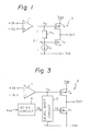
- FIG. 1 is a detailed circuit diagram of Fig. 1 (See Fig. 4 of Japanese Unexamined Patent Publication No. 59-156012).
- reference numeral 1 designates a differential amplifier circuit for generating an output V2 in accordance with a difference in potential between input signals +IN and -IN, and this circuit 1 comprises P-channel transistors T1 and T2 , N-channel transistors T3 and T4 , and a constant current source I1. Note that a common gate potential is applied to the gates of the P-channel transistors T1 and T2 , thereby forming a current mirror circuit.
- the N-channel transistors T3 and T4 are operated in a saturation state. For example, if +IN > -IN, a voltage V1 is high and a voltage V2 is low. Conversely, if +IN ⁇ -IN, the voltage V1 is low and the voltage V2 is high. In this case, the center of an amplitude of the signals +IN and -IN is at an intermediate level between two power supply voltages V DD and V SS .
- Reference numeral 2 designates a level shift circuit for shifting down the output voltage V2 of the differential amplifier circuit 1 by a predetermined voltage, and this circuit 2 comprises an N-channel transistor T5 and a constant current source I2.
- the difference between the output voltage V2 of the differential amplifier circuit 1 and the output voltage V3 of the level shift circuit 2 is determined by the threshold voltage of the N-channel transistor T5 , the characteristics ⁇ of the transistor T5 , and the current of the constant current source I2.
- Reference numeral 3 designated a push-pull output circuit which is composed of a series circuit formed by a P-channel transistor T6 and a N-channel transistor T7.
- Reference C C designates a phase compensating capacitor used to avoid oscillation due to a negative feedback circuit.
- a current flowing through the transistor T6 is determined by the difference between V DD and V2
- a current flowing through the transistor T7 is determined by the difference between V3 and V SS .
- the value (V2 - V3) is constant.
- V DD - V SS (V DD - V2) + (V2 - V3) + (V3 - V SS ) Therefore, if (V DD - V SS ) is greatly fluctuated, the first term (V DD - V2) and the third term (V3 - V SS ) are greatly fluctuated, since the second term (V2 - V3) is constant.
- the first term affects the conductivity of the P-channel transistor T6 and the third term affects the conductivity of the N-channel transistor T7 , thus greatly affecting the operating point of the push-pull output circuit 3, which means that the output voltage at the terminal OUT of the push-pull output circuit 3 is greatly fluctuated. Also, if the operating point of the push-pull output circuit 3 is fluctuated, the supply current and the characteristics of the unity gain and the DC gain are also fluctuated.
- a bias circuit 4 is added to the elements of Fig. 1, and the level shift circuit 2 is modified. Namely, the bias circuit 4 generates a bias voltage V B in accordance with the fluctuation of the power supply voltage V DD to control the level shift circuit 2, and thus the output voltage of the level shift circuit 2 is not changed even when the fluctuation of the power supply voltage V DD occurs. That is, the bias circuit 4 controls the level shift circuit 2 by the bias voltage V B having a fluctuation in accordance with the fluctuation of the power supply voltage V DD .
- the fluctuation of the power supply voltage V DD does not affect the gate-to-source (V3 - V SS ) of the transistor T7 of the push-pull output circuit 3, and therefore, even if the power supply voltage V DD is fluctuated, the current flowing through the transistor T7 is not fluctuated.
- the output voltage V2 of the differential amplifier circuit 1 follows the power supply voltage V DD , the voltage (V DD - V2) is not fluctuated even when the power supply voltage V DD is fluctuated, and therefore, the current flowing through the transistor T6 is not fluctuated. Accordingly, the operating point of the push-pull output circuit 3 is not fluctuated by the fluctuation of the power supply voltage V DD .
- Fig. 4 which illustrates a first embodiment of the present invention
- the constant current source I2 of the level shift circuit 2 of Fig. 2 is replaced by an N-channel transistor T8 serving as a variable current source, and the gate thereof is controlled by the bias voltage V B of the bias circuit 4.
- the bias circuit 4 comprises a P-channel transistor T1, corresponding to the P-channel transistor T1 and T2 of the differential amplifier circuit 1, a constant current source I1′ corresponding to the constant current source I1 , an N-channel transistor T5′ corresponding to the N-channel transistor T5 of the level shift circuit 2, and a N-channel transistor T8′ and a constant current source T8′ corresponding to the N-channel transistor T8.
- the constituents of the bias circuit 4 are determined so that the fluctuation ⁇ V3 of the output voltage V3 of the level shift circuit 2 is 0 even when a fluctuation ⁇ V DD occurs in the power supply voltage V DD .
- g mx and ⁇ x are a mutual conductance and a constant determined by the size, respectively, of a transistor T x and ⁇ V2 , ⁇ V3 , ⁇ V2′, and ⁇ V B are fluctuations of the voltages V2 , V3 , V2′ , and V B , respectively, when a fluctuation ⁇ V DD occurs in the power supply voltage V DD .
- the fluctuation of a current through the transistor T8 is represented by g m8 ⁇ V B , and therefore, in the transistors T5 and T8 , Similarly, in the transistors T5′ and T8′ of the bias circuit 4,
- ⁇ V2 ⁇ V DD (3)
- ⁇ V2 ⁇ V DD (4) Therefore, from the formulae (1) to (4),
- V DD the power supply voltage
- V SS the ground level, and therefore, no fluctuation occurs in V SS .
- the constituents of the bias circuit 4 are balanced with those of the differential amplifier circuit 1 and the level shift circuit 2.
- the drain-to-source current I D is the same, and in the transistors T8 and T8′, V GS is the same.
- Fig. 6 which illustrates a second embodiment of the present invention
- the transistor T8′ of the bias circuit 4 of Fig. 4 is replaced by a constant current source I8 provided in the level shift circuit 2.
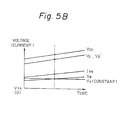
- the voltages of the circuit of Fig. 6 are changed with respect to the change ⁇ V DD , as illustrated in Figs. 7A and 7B.
- the threshold voltage of the N-channel transistor T5 as a constant voltage element is varied by changing the substrate potential due to the back bias effect. That is, in a CMOS circuit, usually an N-channel transistor is formed within a P-conductivity type well, and accordingly, the threshold voltage of the N-channel transistor T5 can be changed by changing the potential of the P-conductivity type well, and thus the voltage (V2 - V3) can be varied.
- the substrate potential of the transistor T5 is controlled by the output voltage V B of the bias circuit 4.
- the operating point of the transistor T7 is In Fig. 8, when the power supply voltage V DD is changed by ⁇ V DD , the voltages V2 and V2′ are also changed by ⁇ V DD .
- the voltages V3 and V3′ have the same tendency to change.
- the currents through the transistors T7 and T7′ tend to increase, and as a result, the back bias potential V B of the transistors T5′ and T5 reduced. Therefore, the threshold voltages of the transistors T5′ and T5 are increased to suppress the increase of the voltages V3 and V3′.
- the currents of the transistors T7 and T7′ tend to decrease, and as a result, the back bias potential V B of the transistors T5′ and T5 is increased.
- the threshold voltages of the transistors T5′ and T5 is decreased to suppress the decrease of the voltages V3 and V3′. Therefore, even when a fluctuation ⁇ V DD occurs in the power supply voltage V DD , the fluctuation ⁇ V3 of the voltage V3 can be 0.
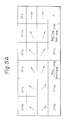
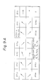
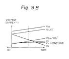
- the voltages are changed with respect to the change ⁇ V DD as illustrated in Figs. 9A and 9B.
- the transistors and constant current sources of the bias circuit have a configuration similar to that of the differential amplifier circuit and level shift circuit of the operational amplifier circuit, the bias condition of the bias circuit is the same as that of the operational amplifier circuit, and thus the operating point can be stabilized with respect to the parameter fluctuation of the transistors.
- the operating point can be stabilized even when fluctuations occur in the power supply voltage, and as a result, the fluctuation of the power current, the fluctuation of the unity gain frequency characteristics, and the fluctuation of the DC gain characteristics are reduced with respect to the change of the power supply voltage.
- the characteristic of a threshold voltage of a transistor with respect to the fluctuations of constants thereof can be stabilized simultaneously with the suppression of the fluctuation of the characteristics with respect to the fluctuation of the characteristics of the power supply voltage. Note, according to results of the inventors, experiments, the fluctuation of the power current is reduced by about 1/4; the fluctuation of the unit gain frequency characteristics is reduced by about 1/2; and the fluctuation of the DC gain characteristics as reduced by about 1/3, compared with the prior art circuit of Figs. 1 and 2.
Landscapes
- Engineering & Computer Science (AREA)
- Power Engineering (AREA)
- Amplifiers (AREA)
Applications Claiming Priority (2)
| Application Number | Priority Date | Filing Date | Title |
|---|---|---|---|
| JP295326/87 | 1987-11-25 | ||
| JP62295326A JP2594585B2 (ja) | 1987-11-25 | 1987-11-25 | 演算増幅回路 |
Publications (3)
| Publication Number | Publication Date |
|---|---|
| EP0318396A2 true EP0318396A2 (de) | 1989-05-31 |
| EP0318396A3 EP0318396A3 (en) | 1990-03-21 |
| EP0318396B1 EP0318396B1 (de) | 1995-02-22 |
Family
ID=17819167
Family Applications (1)
| Application Number | Title | Priority Date | Filing Date |
|---|---|---|---|
| EP88402978A Expired - Lifetime EP0318396B1 (de) | 1987-11-25 | 1988-11-25 | Operationsverstärker mit stabilem Arbeitspunkt |
Country Status (5)
| Country | Link |
|---|---|
| US (1) | US4912425A (de) |
| EP (1) | EP0318396B1 (de) |
| JP (1) | JP2594585B2 (de) |
| KR (1) | KR910001646B1 (de) |
| DE (1) | DE3853136T2 (de) |
Cited By (5)
| Publication number | Priority date | Publication date | Assignee | Title |
|---|---|---|---|---|
| EP0420183A3 (en) * | 1989-09-27 | 1991-08-07 | Kabushiki Kaisha Toshiba | Push-pull circuit |
| US5296754A (en) * | 1989-09-27 | 1994-03-22 | Kabushiki Kaisha Toshiba | Push-pull circuit resistant to power supply and temperature induced distortion |
| EP0604206A1 (de) * | 1992-12-22 | 1994-06-29 | Nec Corporation | Gegentaktverstärkerschaltung |
| EP0688097A3 (de) * | 1994-06-17 | 1997-01-02 | Fujitsu Ltd | Operationsverstärker und Stromdetektorschaltungen |
| EP0790704A1 (de) * | 1996-02-15 | 1997-08-20 | Matsushita Electric Industrial Co., Ltd. | Operationsverstärker |
Families Citing this family (25)
| Publication number | Priority date | Publication date | Assignee | Title |
|---|---|---|---|---|
| JP2790496B2 (ja) * | 1989-11-10 | 1998-08-27 | 富士通株式会社 | 増幅回路 |
| US5057789A (en) * | 1990-07-31 | 1991-10-15 | At&T Bell Laboratories | Class AB CMOS amplifier |
| JP3302030B2 (ja) * | 1990-10-09 | 2002-07-15 | 株式会社東芝 | バッファ回路 |
| IT1247657B (it) * | 1990-12-21 | 1994-12-28 | Sgs Thomson Microelectronics | Amplificatore operazionale cmos di potenza con uscita differenziale. |
| JP3385100B2 (ja) * | 1994-06-17 | 2003-03-10 | 富士通株式会社 | 演算増幅器 |
| JPH0878971A (ja) * | 1994-06-30 | 1996-03-22 | Fujitsu Ltd | 出力回路および演算増幅器 |
| JPH08213850A (ja) * | 1995-02-06 | 1996-08-20 | Fujitsu Ltd | 演算増幅回路 |
| US5684429A (en) * | 1995-09-14 | 1997-11-04 | Ncr Corporation | CMOS gigabit serial link differential transmitter and receiver |
| US5856749A (en) * | 1996-11-01 | 1999-01-05 | Burr-Brown Corporation | Stable output bias current circuitry and method for low-impedance CMOS output stage |
| US5900783A (en) * | 1997-08-04 | 1999-05-04 | Tritech Microelectronics, Ltd. | Low voltage class AB output stage CMOS operational amplifiers |
| US6028479A (en) * | 1998-01-07 | 2000-02-22 | Plato Labs, Inc. | Low voltage transmission line driver |
| JP3875392B2 (ja) * | 1998-02-23 | 2007-01-31 | 株式会社東芝 | 演算増幅器 |
| US6259316B1 (en) * | 1998-05-29 | 2001-07-10 | Texas Instruments Incorporated | Low voltage buffer amplifier for high speed sample and hold applications |
| JP3600175B2 (ja) * | 2000-03-23 | 2004-12-08 | 株式会社東芝 | 増幅装置及び液晶表示装置 |
| US6535062B1 (en) * | 2000-06-30 | 2003-03-18 | Raytheon Company | Low noise, low distortion, complementary IF amplifier |
| DE10128772B4 (de) * | 2001-06-13 | 2009-10-15 | Infineon Technologies Ag | Verfahren und Vorrichtung zur Einschaltstrombegrenzung in Gegentaktverstärkerendstufen |
| DE10161347C1 (de) * | 2001-12-13 | 2003-04-17 | Texas Instruments Deutschland | Schaltungsanordnung zum Umsetzen eines differentiellen Eingangs-Taktsignalpaars in ein unsymmetrisches Ausgangstaktsignal |
| US7078971B2 (en) * | 2004-11-19 | 2006-07-18 | Potentia Semiconductor Inc. | Class AB CMOS amplifiers |
| US7768349B2 (en) | 2006-08-21 | 2010-08-03 | Asahi Kasei Emd Corporation | Transconductance amplifier |
| KR101113378B1 (ko) | 2006-08-28 | 2012-03-13 | 아사히 가세이 일렉트로닉스 가부시끼가이샤 | 트랜스컨덕턴스 증폭기 |
| US7622990B2 (en) * | 2006-08-30 | 2009-11-24 | Micron Technology, Inc. | Amplifiers, methods of increasing current gain in amplifiers, and imaging devices |
| DE602008001800D1 (de) * | 2007-03-29 | 2010-08-26 | Nxp Bv | Verbesserter verstärker |
| US7570116B2 (en) * | 2007-05-10 | 2009-08-04 | Analog Devices, Inc. | Output stage |
| CN101471628B (zh) * | 2007-12-24 | 2012-02-08 | 瑞昱半导体股份有限公司 | Ab类放大器 |
| US8536947B2 (en) * | 2008-12-19 | 2013-09-17 | Qualcomm Incorporated | Class AB amplifier with resistive level-shifting circuitry |
Family Cites Families (8)
| Publication number | Priority date | Publication date | Assignee | Title |
|---|---|---|---|---|
| US3609414A (en) * | 1968-08-20 | 1971-09-28 | Ibm | Apparatus for stabilizing field effect transistor thresholds |
| US4284957A (en) * | 1979-09-28 | 1981-08-18 | American Microsystems, Inc. | CMOS Operational amplifier with reduced power dissipation |
| US4379267A (en) * | 1980-06-25 | 1983-04-05 | Mostek Corporation | Low power differential amplifier |
| JPS59156012A (ja) * | 1983-02-25 | 1984-09-05 | Sony Corp | 演算増幅器 |
| JPS59196613A (ja) * | 1983-04-21 | 1984-11-08 | Toshiba Corp | 演算増幅回路 |
| DE3405809C2 (de) * | 1984-02-17 | 1986-08-14 | Texas Instruments Deutschland Gmbh, 8050 Freising | Ausgangsstufe |
| DE3480044D1 (en) * | 1984-12-28 | 1989-11-09 | Ibm | Constant biasing circuit and operational amplifier using said circuit |
| JPS6245203A (ja) * | 1985-08-23 | 1987-02-27 | Hitachi Ltd | Mos増幅出力回路 |
-
1987
- 1987-11-25 JP JP62295326A patent/JP2594585B2/ja not_active Expired - Fee Related
-
1988
- 1988-11-23 US US07/275,311 patent/US4912425A/en not_active Expired - Lifetime
- 1988-11-24 KR KR8815494A patent/KR910001646B1/ko not_active Expired
- 1988-11-25 EP EP88402978A patent/EP0318396B1/de not_active Expired - Lifetime
- 1988-11-25 DE DE3853136T patent/DE3853136T2/de not_active Expired - Fee Related
Cited By (9)
| Publication number | Priority date | Publication date | Assignee | Title |
|---|---|---|---|---|
| EP0420183A3 (en) * | 1989-09-27 | 1991-08-07 | Kabushiki Kaisha Toshiba | Push-pull circuit |
| US5296754A (en) * | 1989-09-27 | 1994-03-22 | Kabushiki Kaisha Toshiba | Push-pull circuit resistant to power supply and temperature induced distortion |
| EP0604206A1 (de) * | 1992-12-22 | 1994-06-29 | Nec Corporation | Gegentaktverstärkerschaltung |
| EP0688097A3 (de) * | 1994-06-17 | 1997-01-02 | Fujitsu Ltd | Operationsverstärker und Stromdetektorschaltungen |
| US5606287A (en) * | 1994-06-17 | 1997-02-25 | Fujitsu Limited | Operational amplifier having stable operations for a wide range of source voltage, and current detector circuit employing a small number of elements |
| EP1104108A1 (de) * | 1994-06-17 | 2001-05-30 | Fujitsu Limited | Stromdetektorschaltungen |
| USRE37217E1 (en) * | 1994-06-17 | 2001-06-12 | Fujitsu Limited | Operational amplifier having stable operations for a wide range of source voltage, and current detector circuit employing a small number of elements |
| EP0790704A1 (de) * | 1996-02-15 | 1997-08-20 | Matsushita Electric Industrial Co., Ltd. | Operationsverstärker |
| US5933055A (en) * | 1996-02-15 | 1999-08-03 | Matsushita Electric Industrial Co., Ltd. | Operational amplifier operable with high performance even at a low voltage |
Also Published As
| Publication number | Publication date |
|---|---|
| DE3853136D1 (de) | 1995-03-30 |
| JPH01137808A (ja) | 1989-05-30 |
| DE3853136T2 (de) | 1995-06-14 |
| US4912425A (en) | 1990-03-27 |
| KR890009072A (ko) | 1989-07-15 |
| EP0318396B1 (de) | 1995-02-22 |
| JP2594585B2 (ja) | 1997-03-26 |
| EP0318396A3 (en) | 1990-03-21 |
| KR910001646B1 (en) | 1991-03-16 |
Similar Documents
| Publication | Publication Date | Title |
|---|---|---|
| EP0318396B1 (de) | Operationsverstärker mit stabilem Arbeitspunkt | |
| US5907259A (en) | Operational amplification circuit capable of driving a high load | |
| US5767748A (en) | Voltage controlled oscillator and voltage controlled delay circuit | |
| US7187235B2 (en) | Class AB rail-to-rail operational amplifier | |
| US4933644A (en) | Common-mode feedback bias generator for operational amplifiers | |
| US6466070B1 (en) | Low voltage charge pump | |
| US5959446A (en) | High swing current efficient CMOS cascode current mirror | |
| US4069431A (en) | Amplifier circuit | |
| EP0380152A1 (de) | Transistorschaltung | |
| US20050007195A1 (en) | Low voltage high gain amplifier circuits | |
| EP0310135B1 (de) | Operationsverstärker | |
| US4658157A (en) | IGFET comparator circuit having greater control of intended offset voltage | |
| US6005440A (en) | Operational amplifier | |
| US5543745A (en) | Voltage controlled current source and bias generation circuit using such current source | |
| US6344769B1 (en) | Precision differential switched current source | |
| US4628280A (en) | Amplifier arrangement | |
| US5793239A (en) | Composite load circuit | |
| JP3234732B2 (ja) | レベル変換回路 | |
| KR20060056419A (ko) | Am 중간 주파 가변 이득 증폭 회로, 가변 이득 증폭 회로및 그 반도체 집적 회로 | |
| US5287068A (en) | Comparator amplifier | |
| EP0361529A2 (de) | Spannungsgesteuerter Oszillator | |
| US5221910A (en) | Single-pin amplifier in integrated circuit form | |
| US6985038B2 (en) | Operational amplifier generating desired feedback reference voltage allowing improved output characteristic | |
| US4446444A (en) | CMOS Amplifier | |
| US6060940A (en) | CMOS output stage for providing stable quiescent current |
Legal Events
| Date | Code | Title | Description |
|---|---|---|---|
| PUAI | Public reference made under article 153(3) epc to a published international application that has entered the european phase |
Free format text: ORIGINAL CODE: 0009012 |
|
| AK | Designated contracting states |
Kind code of ref document: A2 Designated state(s): DE FR GB |
|
| PUAL | Search report despatched |
Free format text: ORIGINAL CODE: 0009013 |
|
| AK | Designated contracting states |
Kind code of ref document: A3 Designated state(s): DE FR GB |
|
| 17P | Request for examination filed |
Effective date: 19900910 |
|
| 17Q | First examination report despatched |
Effective date: 19930507 |
|
| GRAA | (expected) grant |
Free format text: ORIGINAL CODE: 0009210 |
|
| AK | Designated contracting states |
Kind code of ref document: B1 Designated state(s): DE FR GB |
|
| REF | Corresponds to: |
Ref document number: 3853136 Country of ref document: DE Date of ref document: 19950330 |
|
| ET | Fr: translation filed | ||
| PGFP | Annual fee paid to national office [announced via postgrant information from national office to epo] |
Ref country code: GB Payment date: 19951114 Year of fee payment: 8 |
|
| PLBE | No opposition filed within time limit |
Free format text: ORIGINAL CODE: 0009261 |
|
| STAA | Information on the status of an ep patent application or granted ep patent |
Free format text: STATUS: NO OPPOSITION FILED WITHIN TIME LIMIT |
|
| PGFP | Annual fee paid to national office [announced via postgrant information from national office to epo] |
Ref country code: DE Payment date: 19960124 Year of fee payment: 8 |
|
| 26N | No opposition filed | ||
| PG25 | Lapsed in a contracting state [announced via postgrant information from national office to epo] |
Ref country code: GB Effective date: 19961125 |
|
| GBPC | Gb: european patent ceased through non-payment of renewal fee |
Effective date: 19961125 |
|
| PG25 | Lapsed in a contracting state [announced via postgrant information from national office to epo] |
Ref country code: DE Effective date: 19970801 |
|
| PGFP | Annual fee paid to national office [announced via postgrant information from national office to epo] |
Ref country code: FR Payment date: 20031110 Year of fee payment: 16 |
|
| PG25 | Lapsed in a contracting state [announced via postgrant information from national office to epo] |
Ref country code: FR Free format text: LAPSE BECAUSE OF NON-PAYMENT OF DUE FEES Effective date: 20050729 |
|
| REG | Reference to a national code |
Ref country code: FR Ref legal event code: ST |