EP0318883A1 - Coupleur optique monolithique - Google Patents
Coupleur optique monolithique Download PDFInfo
- Publication number
- EP0318883A1 EP0318883A1 EP88119766A EP88119766A EP0318883A1 EP 0318883 A1 EP0318883 A1 EP 0318883A1 EP 88119766 A EP88119766 A EP 88119766A EP 88119766 A EP88119766 A EP 88119766A EP 0318883 A1 EP0318883 A1 EP 0318883A1
- Authority
- EP
- European Patent Office
- Prior art keywords
- substrate
- components
- layer
- layers
- monolithic
- Prior art date
- Legal status (The legal status is an assumption and is not a legal conclusion. Google has not performed a legal analysis and makes no representation as to the accuracy of the status listed.)
- Granted
Links
- 239000000306 component Substances 0.000 claims abstract description 76
- 239000000758 substrate Substances 0.000 claims abstract description 52
- 230000005855 radiation Effects 0.000 claims abstract description 23
- 230000003287 optical effect Effects 0.000 claims abstract description 18
- 238000012216 screening Methods 0.000 claims abstract description 13
- 229910052751 metal Inorganic materials 0.000 claims description 15
- 239000002184 metal Substances 0.000 claims description 15
- 239000000463 material Substances 0.000 claims description 9
- 239000004065 semiconductor Substances 0.000 claims description 4
- 229920000136 polysorbate Polymers 0.000 claims 1
- 238000004519 manufacturing process Methods 0.000 abstract description 12
- 238000000034 method Methods 0.000 abstract description 4
- 239000010410 layer Substances 0.000 description 53
- 239000004020 conductor Substances 0.000 description 5
- 230000005540 biological transmission Effects 0.000 description 4
- 238000005229 chemical vapour deposition Methods 0.000 description 4
- 238000004943 liquid phase epitaxy Methods 0.000 description 4
- JBRZTFJDHDCESZ-UHFFFAOYSA-N AsGa Chemical compound [As]#[Ga] JBRZTFJDHDCESZ-UHFFFAOYSA-N 0.000 description 3
- 229910001218 Gallium arsenide Inorganic materials 0.000 description 3
- 238000005530 etching Methods 0.000 description 3
- VYPSYNLAJGMNEJ-UHFFFAOYSA-N Silicium dioxide Chemical compound O=[Si]=O VYPSYNLAJGMNEJ-UHFFFAOYSA-N 0.000 description 2
- 230000000903 blocking effect Effects 0.000 description 2
- 238000010292 electrical insulation Methods 0.000 description 2
- 239000011810 insulating material Substances 0.000 description 2
- 239000012212 insulator Substances 0.000 description 2
- 238000001465 metallisation Methods 0.000 description 2
- 230000008054 signal transmission Effects 0.000 description 2
- GYHNNYVSQQEPJS-UHFFFAOYSA-N Gallium Chemical compound [Ga] GYHNNYVSQQEPJS-UHFFFAOYSA-N 0.000 description 1
- 241000951490 Hylocharis chrysura Species 0.000 description 1
- 229910052782 aluminium Inorganic materials 0.000 description 1
- XAGFODPZIPBFFR-UHFFFAOYSA-N aluminium Chemical compound [Al] XAGFODPZIPBFFR-UHFFFAOYSA-N 0.000 description 1
- 229910052729 chemical element Inorganic materials 0.000 description 1
- 239000011248 coating agent Substances 0.000 description 1
- 238000000576 coating method Methods 0.000 description 1
- 229910052681 coesite Inorganic materials 0.000 description 1
- 229910052906 cristobalite Inorganic materials 0.000 description 1
- 238000011161 development Methods 0.000 description 1
- 230000018109 developmental process Effects 0.000 description 1
- 229910052733 gallium Inorganic materials 0.000 description 1
- 238000001451 molecular beam epitaxy Methods 0.000 description 1
- 239000012071 phase Substances 0.000 description 1
- 229910052594 sapphire Inorganic materials 0.000 description 1
- 239000010980 sapphire Substances 0.000 description 1
- 238000000926 separation method Methods 0.000 description 1
- 239000000377 silicon dioxide Substances 0.000 description 1
- 235000012239 silicon dioxide Nutrition 0.000 description 1
- 229910052682 stishovite Inorganic materials 0.000 description 1
- 239000012780 transparent material Substances 0.000 description 1
- 229910052905 tridymite Inorganic materials 0.000 description 1
Images


Classifications
-
- H—ELECTRICITY
- H04—ELECTRIC COMMUNICATION TECHNIQUE
- H04B—TRANSMISSION
- H04B10/00—Transmission systems employing electromagnetic waves other than radio-waves, e.g. infrared, visible or ultraviolet light, or employing corpuscular radiation, e.g. quantum communication
- H04B10/80—Optical aspects relating to the use of optical transmission for specific applications, not provided for in groups H04B10/03 - H04B10/70, e.g. optical power feeding or optical transmission through water
- H04B10/801—Optical aspects relating to the use of optical transmission for specific applications, not provided for in groups H04B10/03 - H04B10/70, e.g. optical power feeding or optical transmission through water using optical interconnects, e.g. light coupled isolators, circuit board interconnections
- H04B10/802—Optical aspects relating to the use of optical transmission for specific applications, not provided for in groups H04B10/03 - H04B10/70, e.g. optical power feeding or optical transmission through water using optical interconnects, e.g. light coupled isolators, circuit board interconnections for isolation, e.g. using optocouplers
-
- G—PHYSICS
- G02—OPTICS
- G02B—OPTICAL ELEMENTS, SYSTEMS OR APPARATUS
- G02B6/00—Light guides; Structural details of arrangements comprising light guides and other optical elements, e.g. couplings
- G02B6/24—Coupling light guides
- G02B6/42—Coupling light guides with opto-electronic elements
- G02B6/4201—Packages, e.g. shape, construction, internal or external details
- G02B6/4246—Bidirectionally operating package structures
-
- G—PHYSICS
- G02—OPTICS
- G02B—OPTICAL ELEMENTS, SYSTEMS OR APPARATUS
- G02B6/00—Light guides; Structural details of arrangements comprising light guides and other optical elements, e.g. couplings
- G02B6/24—Coupling light guides
- G02B6/42—Coupling light guides with opto-electronic elements
- G02B6/4295—Coupling light guides with opto-electronic elements coupling with semiconductor devices activated by light through the light guide, e.g. thyristors, phototransistors
-
- H—ELECTRICITY
- H10—SEMICONDUCTOR DEVICES; ELECTRIC SOLID-STATE DEVICES NOT OTHERWISE PROVIDED FOR
- H10F—INORGANIC SEMICONDUCTOR DEVICES SENSITIVE TO INFRARED RADIATION, LIGHT, ELECTROMAGNETIC RADIATION OF SHORTER WAVELENGTH OR CORPUSCULAR RADIATION
- H10F55/00—Radiation-sensitive semiconductor devices covered by groups H10F10/00, H10F19/00 or H10F30/00 being structurally associated with electric light sources and electrically or optically coupled thereto
- H10F55/18—Radiation-sensitive semiconductor devices covered by groups H10F10/00, H10F19/00 or H10F30/00 being structurally associated with electric light sources and electrically or optically coupled thereto wherein the radiation-sensitive semiconductor devices and the electric light source share a common body having dual-functionality of light emission and light detection
-
- H—ELECTRICITY
- H10—SEMICONDUCTOR DEVICES; ELECTRIC SOLID-STATE DEVICES NOT OTHERWISE PROVIDED FOR
- H10F—INORGANIC SEMICONDUCTOR DEVICES SENSITIVE TO INFRARED RADIATION, LIGHT, ELECTROMAGNETIC RADIATION OF SHORTER WAVELENGTH OR CORPUSCULAR RADIATION
- H10F55/00—Radiation-sensitive semiconductor devices covered by groups H10F10/00, H10F19/00 or H10F30/00 being structurally associated with electric light sources and electrically or optically coupled thereto
- H10F55/20—Radiation-sensitive semiconductor devices covered by groups H10F10/00, H10F19/00 or H10F30/00 being structurally associated with electric light sources and electrically or optically coupled thereto wherein the electric light source controls the radiation-sensitive semiconductor devices, e.g. optocouplers
- H10F55/25—Radiation-sensitive semiconductor devices covered by groups H10F10/00, H10F19/00 or H10F30/00 being structurally associated with electric light sources and electrically or optically coupled thereto wherein the electric light source controls the radiation-sensitive semiconductor devices, e.g. optocouplers wherein the radiation-sensitive devices and the electric light source are all semiconductor devices
- H10F55/255—Radiation-sensitive semiconductor devices covered by groups H10F10/00, H10F19/00 or H10F30/00 being structurally associated with electric light sources and electrically or optically coupled thereto wherein the electric light source controls the radiation-sensitive semiconductor devices, e.g. optocouplers wherein the radiation-sensitive devices and the electric light source are all semiconductor devices formed in, or on, a common substrate
Definitions
- the present invention relates to a monolithic optocoupler according to the introductory part of claim 1.
- An optocoupler comprises an optical signal transmitter, e.g. a light-emitting diode or laser diode, and an optical signal receiver, e.g. a photo-diode or photo-transistor.
- the signal transmitter is connected to a first electrical circuit and the signal receiver to a second electrical circuit.
- a signal from the first circuit is converted to an optical signal in the signal transmitter.
- This optical signal is transmitted in the form of optical radiation to the signal receiver, where it is converted to an electrical signal and then supplied to the second circuit.
- the optocoupler is generally designed as one component including the signal transmitter and the signal receiver, suitable radiation-transfer means (e.g. in the form of light guides or mirrors) and electrically insulating means to galvanically separate the two circuits.
- suitable radiation-transfer means e.g. in the form of light guides or mirrors
- electrically insulating means to galvanically separate the two circuits.
- Both information and power can be transmitted from one circuit to the other with the aid of an optocoupler.
- Separate optocouplers may be used for the different signals if signals are to be transmitted in both directions. Alternatively a single optocoupler may be used for two-way transmission of signals and/or power, in which case each of the optical components is designed to operate optionally as emitter or receiver of optical radiation.
- An optocoupler is often required to have small dimensions. It is then suitably produced in the form of a monolithic optocoupler, using the integrated-circuit technique.
- the two electro-optical components are then arranged on a common substrate.
- the layers which together form the two components are successively produced during manufacture on the substrate by means of liquid phase epitaxy (LPE), molecular beam epitaxy (MBE) or chemical vapour deposition (CVD), for instance.
- LPE liquid phase epitaxy
- MBE molecular beam epitaxy
- CVD chemical vapour deposition
- the substrate may consist of a good insulator, e.g. sapphire, or - which has been found to have several advantages - of a "semi-insulating" material, preferably of the same type, e.g. gallium arsenide, as the material of which the two components are made.
- the resistivity of a semi-insulating material may be within the range 107-1012 ohmcm.
- Optocouplers of this type are previously known through US-A-4 212 020 and PTC application WO 85/04491.
- An optocoupler is already known through US-A-4 021 834, in which both optical components are applied on a common substrate.
- the substrate consists of gallium arsenide and has a strongly n-doped, and thus low-resistive, part extending between the two components.
- the two components are electrically insulated from each other since they are arranged on SiO2 layers on the surface of the substrate. Since in practice these layers can only be made thin, their breakthrough voltage will be low, and this known optocoupler can therefore only be used for extremely low voltages.
- the optical radiation can be transmitted in known manner from the transmitting to the receiving component in various ways.
- Mirroring or total-reflecting members may be arranged to ensure that as much radiation from the emitter as possible reaches the receiver.
- a transparent layer acting as waveguide may be arranged between the two components.
- the substrate may be used as waveguide for the optical radiation, and utilized as such.
- the invention aims to develop a monolithic optocoupler of the above-mentioned kind, which exhibits both, a considerable reduction of the above-mentioned interference and sufficient electrical insulation between the two components of the monolithic body, and which optocoupler can be manufac tured at substantially the same costs than the previously known monolithic optocoupler.
- the invention suggests a monolithic optocoupler according to the introductory part of Claim 1, which is characterized by the features of the characterizing part of Claim 1.
- An optocoupler according to the invention offers efficient screening against interference without any extra process steps, or only a minimum of such steps, being required during its manufacture. Efficient screening of both capacitively and resistively transmitted interference can be obtained.
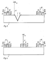
- Figure 1a shows an optocoupler of previously known type.
- the component comprises a substrate 1 carrying the two opto-components A and B.
- the substrate may suitably consist of a thin plate of a semi-insulating material such as gallium arsenide.
- a substrate of this material can have a conductivity within the interval 107-1012 ohmcm, e.g. 108 ohmcm.
- the two opto-components A and B are arranged spaced apart from each other on the substrate. This can be achieved in known manner, such as by liquid phase epitaxy (LPE) or chemical vapour deposition (CVD) of the material in the three layers forming each opto-component.
- LPE liquid phase epitaxy
- CVD chemical vapour deposition
- Component A consist of two p-conducting layers A1 and A2 and an n-conducting layer A3. To ensure good contact the latter two layers are provided with metallizations A4 and A5, to which connection wires A6 and A7 are attached.
- Component A can be utilized either as radiation-emitting diode or as radiation detecting photodiode. In the first case a current is passed in conducting direction through the diode formed by layers A2 and A3, optical radiation then being emitted from the region at the pn-junction between these two layers. In the latter case, said diode is biased in blocking direction and the current flowing in the reverse direction which is generated by the optical radiation is detected by suitable circuits, not shown.
- Component B may be identical to component A.
- Each of the two components can thus operate optionally as emitter or detector of radiation.
- signal transmission may be one-way, in which case one element always functions as radiation emitter and the other element always functions as radiation detector, or it may be two-way, in which case each component functions alternately as emitter and detector for optical radiation.
- the radiation can be transmitted from the transmitting to the receiving component in several ways.
- One way is shown in Figure 1a where the substrate 1 is utilized as waveguide to transmit radiation between the components.
- some form of mirroring member may be arranged above the components, designed in such a manner that as large a part as possible of the radiation emitted from the transmitting element is reflected towards the receiving component.
- Such a mirroring member may consist, for instance, of an approximately semi-spherical body applied on the substrate and encompassing the two components, the spherical surface of this body reflecting the rays either due to total reflection or by the surface being provided with a reflecting coating.
- the substrate may consist, for instance, of an insulator such as sapphire.
- Figure 1b shows schematically how the optocoupler according to Figure 1a is used to connect two electrical circuits 2 and 3.
- the optocoupler is designated OC in Figure 1b.
- A is the transmitting and B the receiving component.
- the circuit 2 causes a current to flow through component A in conducting direction so that the current, and thus the radiation emitted by A, is modulated with the information to be transmitted to circuit 3.
- This radiation is detected by the component B, which is biased in the reverse direction, and with the aid of detecting circuits, known per se, included in circuit 3.
- electrical interference can be transmitted between circuits 2 and 3 via the optocoupler. This may occur either capacitively or resistively. A certain leakage capacitance exists between the two components A and B of the optocoupler, partly through the environment between the two components and partly through the substrate 1. If the substrate is semi-insulating, interference can be transmitted resistively between the components by a current flowing through the substrate. Since the detecting circuits in devices of this type must often be extremely sensitive, this interference may cause serious problems. Since both components A and B are integrated in one and the same unit, and since the dimensions of such a unit may be extremely small, it is difficult or impossible to eliminate the drawbacks caused by the interference by means of conventional screening.
- Figure 2 shows an example of an optocoupler according to the invention. It differs from the optocoupler shown in Figure 1 in that a metal layer 4 is applied on the surface of the substrate 1 and connected via a conductor 5 to an earth connection 6.
- the metal layer 4 is produced by the same technique as the two opto-components, i.e. the metal layer can be produced in the same manufacturing step as the metal layers A4,A5,B4 and B5. Manufacturing an optocoupler according to the invention thus entails negligible complication when compared with the manufacture of previously known optocouplers.
- the metal layer 4 has two functions: Firstly, it effectively gathers any interference currents flowing between the two components A and B. Secondly, the layer 4 serves as a screen which greatly reduces the interference signals transmitted capacitively through the environment and through the substrate between the two components.
- one or more screens may be placed between the opto-components.
- a screen may be placed symmetrically or asymmetrically depending on the interference picture.
- Figure 3 shows an alternative embodiment of an optocoupler according to the invention. It differs from the optocoupler shown in Figure 2 in that a groove 7 is provided in the substrate 1, e.g. by etching, extending transversely across the substrate between the two opto-components.
- the walls of the groove are provided with a screening metal layer 8 which, in the same way as the layer 4 in Figure 2, is connected to an earthed point 6 via an earthing conductor 5. Since etching and metallization are steps which occur in the normal production of the two components of the optocoupler, this embodiment does not either entail any noticeable complication of the production process, nor is it any more expensive. If the groove 7 is made deep in relation to the thickness of the substrate 1, it will form an effective block against resistive transmission of interference through the substrate. If the substrate is used as waveguide between the components, however, a deep groove will impede transmission of the radiation.
- the metallic layer 8 so thin that radiation can pass through it, or by using a layer 8 in the form of a net, grid or the like.
- the groove 7 may be completely or partially filled with an optically transparent material, such as a highly doped and thus electrically highly conductive material of the same type as the substrate material.
- Figure 4 shows another variant of an optocoupler according to the invention.
- the screening member consists of the semiconductor body formed by the three layers 11,12 and 13 and applied on the substrate 1 between the two opto-components A and B.
- layer 11 can suitably be formed simultaneously with layers A1 and B1, layer 12 simultaneously with layer A2 and B2 and layer 13 simultaneously with layers A3 and B3. It might then be advantageous to deposit the layers over the entire surface of the substrate during each of the manufacturing steps producing these three layers.
- the superfluous parts of the layers i.e. the parts between the screening member and the two opto-components, can be removed by etching, for instance.
- earthing is achieved by arranging a metal layer 15 on the layer 13, this layer 15 being connected to an earth point 6 via an earth conductor 5.
- Layer 12 or layer 11 may of course be earthed either alternatively or suplementarily.
- Figure 5 shows a third alternative in which the metal layer 15 is deposited so that it covers the entire screening semiconductor body 11-12-13 and possibly also adjacent parts of the surface of the substrate 1.
- Figure 6 shows another alternative embodiment of an optocoupler according to the invention.
- component A is shown as the light-emitting diode or photodiode formed by the layers A2 and A3.
- the component may consist of additional layers in known manner, such as an additional p-layer of the type shown in Figures 1-5.
- An n-conducting layer A8 and a p-conducting layer A9 are arranged between the component and the substrate 1. This is made in such a manner that two opposing pn-junctions, connected in series, are formed between the active part of the component - that is the pn-junction between layers A2 and A3 - and the substrate.
- the layers A8 and A9 may suitably consist of material of the same type as that used in the opto-components and be produced using the same type of manufacturing steps as those used for the opto-components.
- the screening means according to Figure 6 is earthed by the layer A9 being connected to an earth point 6 by means of a metal layer A10 and an earth conductor 5. This ensures effective reduction of both, capacitively and resistively transmitted interference.
- the layer A9, and suitably also the metal contact A10, may be extended towards the component B.
- a reverse biased pn-junction will always exist between the component A and the substrate, regardless of the polarity of any interference or other voltages occurring.
- the component shown can be used for both one-way and two-way transmission and for optional potentials and levels of the supply and signal voltages. Extra layers may possibly be arranged below component B in the same way as below component A, thus also separating component B from the substrate during operation with the aid of a reverse biased pn-junction.
- One of the layers may be earthed in the same way as for component A.
- Each of the components is then, of course, earthed on its own side of the optocoupler.
Landscapes
- Physics & Mathematics (AREA)
- General Physics & Mathematics (AREA)
- Optics & Photonics (AREA)
- Electromagnetism (AREA)
- Engineering & Computer Science (AREA)
- Computer Networks & Wireless Communication (AREA)
- Signal Processing (AREA)
- Photo Coupler, Interrupter, Optical-To-Optical Conversion Devices (AREA)
- Shielding Devices Or Components To Electric Or Magnetic Fields (AREA)
- Networks Using Active Elements (AREA)
Priority Applications (1)
| Application Number | Priority Date | Filing Date | Title |
|---|---|---|---|
| AT88119766T ATE74230T1 (de) | 1987-12-02 | 1988-11-26 | Monolithischer optokoppler. |
Applications Claiming Priority (2)
| Application Number | Priority Date | Filing Date | Title |
|---|---|---|---|
| SE8704822A SE461491B (sv) | 1987-12-02 | 1987-12-02 | Monolitisk optokopplare |
| SE8704822 | 1987-12-02 |
Publications (2)
| Publication Number | Publication Date |
|---|---|
| EP0318883A1 true EP0318883A1 (fr) | 1989-06-07 |
| EP0318883B1 EP0318883B1 (fr) | 1992-03-25 |
Family
ID=20370479
Family Applications (1)
| Application Number | Title | Priority Date | Filing Date |
|---|---|---|---|
| EP88119766A Expired - Lifetime EP0318883B1 (fr) | 1987-12-02 | 1988-11-26 | Coupleur optique monolithique |
Country Status (6)
| Country | Link |
|---|---|
| US (1) | US4933561A (fr) |
| EP (1) | EP0318883B1 (fr) |
| JP (1) | JPH01196183A (fr) |
| AT (1) | ATE74230T1 (fr) |
| DE (1) | DE3869566D1 (fr) |
| SE (1) | SE461491B (fr) |
Cited By (4)
| Publication number | Priority date | Publication date | Assignee | Title |
|---|---|---|---|---|
| WO1993007647A1 (fr) * | 1991-10-01 | 1993-04-15 | Asea Brown Boveri Ab | Optocoupleur monolithique |
| EP0632509A3 (fr) * | 1993-06-07 | 1995-02-15 | Motorola Inc | Coupleur optique linéaire intégré et sa méthode de fabrication. |
| EP1335507A1 (fr) * | 2002-01-31 | 2003-08-13 | STMicroelectronics S.r.l. | Methode et dispositif pour une excellente isolation galvanique entre deux circuits basse tension dans un isolateur optique |
| EP1150358A4 (fr) * | 1999-10-12 | 2008-07-02 | Furukawa Electric Co Ltd | Module optique |
Families Citing this family (9)
| Publication number | Priority date | Publication date | Assignee | Title |
|---|---|---|---|---|
| US5357122A (en) * | 1991-09-05 | 1994-10-18 | Sony Corporation | Three-dimensional optical-electronic integrated circuit device with raised sections |
| US5237434A (en) * | 1991-11-05 | 1993-08-17 | Mcnc | Microelectronic module having optical and electrical interconnects |
| JP2513976B2 (ja) * | 1991-12-13 | 1996-07-10 | エイ・ティ・アンド・ティ・コーポレーション | 複数の球状部品の被覆方法 |
| US5285078A (en) * | 1992-01-24 | 1994-02-08 | Nippon Steel Corporation | Light emitting element with employment of porous silicon and optical device utilizing light emitting element |
| US5321294A (en) * | 1992-08-31 | 1994-06-14 | Matsushita Electric Industrial Co., Ltd. | Shift register having optically bistable elements coupled by an optical waveguide layer |
| US5438210A (en) * | 1993-10-22 | 1995-08-01 | Worley; Eugene R. | Optical isolation connections using integrated circuit techniques |
| ES2102937B1 (es) * | 1994-03-07 | 1998-04-01 | Telefonica Nacional Espana Co | Circuito transmisor-receptor. |
| JP4553026B2 (ja) * | 2008-03-27 | 2010-09-29 | 富士ゼロックス株式会社 | 光伝送装置 |
| KR102672299B1 (ko) * | 2016-05-17 | 2024-06-04 | 더 유니버시티 오브 홍콩 | 자체(in situ) 실시간 강도 모니터링을 위한 일체형으로 통합된 광감지기들을 구비한 발광 다이오드(LED) |
Citations (7)
| Publication number | Priority date | Publication date | Assignee | Title |
|---|---|---|---|---|
| US3748480A (en) * | 1970-11-02 | 1973-07-24 | Motorola Inc | Monolithic coupling device including light emitter and light sensor |
| US3881113A (en) * | 1973-12-26 | 1975-04-29 | Ibm | Integrated optically coupled light emitter and sensor |
| US4021834A (en) * | 1975-12-31 | 1977-05-03 | The United States Of America As Represented By The Secretary Of The Army | Radiation-resistant integrated optical signal communicating device |
| US4104533A (en) * | 1977-02-28 | 1978-08-01 | The United States Of America As Represented By The Secretary Of The Navy | Wideband optical isolator |
| US4212020A (en) * | 1978-07-21 | 1980-07-08 | California Institute Of Technology | Solid state electro-optical devices on a semi-insulating substrate |
| US4274104A (en) * | 1979-05-21 | 1981-06-16 | International Business Machines Corporation | Electrooptical integrated circuit communication |
| WO1985004491A1 (fr) * | 1984-03-30 | 1985-10-10 | Louis Menigaux | Procede de fabrication d'un dispositif optique integre monolithique comprenant un laser a semiconducteur et dispositif obtenu par ce procede |
Family Cites Families (10)
| Publication number | Priority date | Publication date | Assignee | Title |
|---|---|---|---|---|
| US3436548A (en) * | 1964-06-29 | 1969-04-01 | Texas Instruments Inc | Combination p-n junction light emitter and photocell having electrostatic shielding |
| DE1614865A1 (de) * | 1967-09-27 | 1970-12-23 | Telefunken Patent | Optoelektronische Halbleiteranordnung |
| US3818451A (en) * | 1972-03-15 | 1974-06-18 | Motorola Inc | Light-emitting and light-receiving logic array |
| JPS5250184A (en) * | 1975-10-20 | 1977-04-21 | Matsushita Electric Ind Co Ltd | Photo coupler |
| US4112308A (en) * | 1976-03-29 | 1978-09-05 | Burr-Brown Research Corporation | Optical coupling system |
| JPS56131973A (en) * | 1980-03-19 | 1981-10-15 | Matsushita Electronics Corp | Luminiscent device |
| JPS5967671A (ja) * | 1982-10-12 | 1984-04-17 | Nec Corp | 発光受光素子 |
| JPS59180514A (ja) * | 1983-03-31 | 1984-10-13 | Toshiba Corp | 光受信モジユ−ル |
| JPS61159776A (ja) * | 1985-01-04 | 1986-07-19 | Oki Electric Ind Co Ltd | 光制御非直線素子 |
| JPS6223181A (ja) * | 1985-07-23 | 1987-01-31 | Matsushita Electric Ind Co Ltd | 光集積化素子 |
-
1987
- 1987-12-02 SE SE8704822A patent/SE461491B/sv not_active IP Right Cessation
-
1988
- 1988-11-26 EP EP88119766A patent/EP0318883B1/fr not_active Expired - Lifetime
- 1988-11-26 DE DE8888119766T patent/DE3869566D1/de not_active Expired - Fee Related
- 1988-11-26 AT AT88119766T patent/ATE74230T1/de not_active IP Right Cessation
- 1988-12-01 JP JP63305103A patent/JPH01196183A/ja active Pending
- 1988-12-02 US US07/278,895 patent/US4933561A/en not_active Expired - Lifetime
Patent Citations (7)
| Publication number | Priority date | Publication date | Assignee | Title |
|---|---|---|---|---|
| US3748480A (en) * | 1970-11-02 | 1973-07-24 | Motorola Inc | Monolithic coupling device including light emitter and light sensor |
| US3881113A (en) * | 1973-12-26 | 1975-04-29 | Ibm | Integrated optically coupled light emitter and sensor |
| US4021834A (en) * | 1975-12-31 | 1977-05-03 | The United States Of America As Represented By The Secretary Of The Army | Radiation-resistant integrated optical signal communicating device |
| US4104533A (en) * | 1977-02-28 | 1978-08-01 | The United States Of America As Represented By The Secretary Of The Navy | Wideband optical isolator |
| US4212020A (en) * | 1978-07-21 | 1980-07-08 | California Institute Of Technology | Solid state electro-optical devices on a semi-insulating substrate |
| US4274104A (en) * | 1979-05-21 | 1981-06-16 | International Business Machines Corporation | Electrooptical integrated circuit communication |
| WO1985004491A1 (fr) * | 1984-03-30 | 1985-10-10 | Louis Menigaux | Procede de fabrication d'un dispositif optique integre monolithique comprenant un laser a semiconducteur et dispositif obtenu par ce procede |
Cited By (4)
| Publication number | Priority date | Publication date | Assignee | Title |
|---|---|---|---|---|
| WO1993007647A1 (fr) * | 1991-10-01 | 1993-04-15 | Asea Brown Boveri Ab | Optocoupleur monolithique |
| EP0632509A3 (fr) * | 1993-06-07 | 1995-02-15 | Motorola Inc | Coupleur optique linéaire intégré et sa méthode de fabrication. |
| EP1150358A4 (fr) * | 1999-10-12 | 2008-07-02 | Furukawa Electric Co Ltd | Module optique |
| EP1335507A1 (fr) * | 2002-01-31 | 2003-08-13 | STMicroelectronics S.r.l. | Methode et dispositif pour une excellente isolation galvanique entre deux circuits basse tension dans un isolateur optique |
Also Published As
| Publication number | Publication date |
|---|---|
| JPH01196183A (ja) | 1989-08-07 |
| EP0318883B1 (fr) | 1992-03-25 |
| SE8704822D0 (sv) | 1987-12-02 |
| ATE74230T1 (de) | 1992-04-15 |
| DE3869566D1 (de) | 1992-04-30 |
| US4933561A (en) | 1990-06-12 |
| SE461491B (sv) | 1990-02-19 |
| SE8704822L (sv) | 1989-06-03 |
Similar Documents
| Publication | Publication Date | Title |
|---|---|---|
| EP0318883A1 (fr) | Coupleur optique monolithique | |
| US4766471A (en) | Thin film electro-optical devices | |
| CA1207419A (fr) | Photocapteur | |
| US6774448B1 (en) | High speed detectors having integrated electrical components | |
| US4899204A (en) | High voltage switch structure with light responsive diode stack | |
| US6670600B2 (en) | Semiconductor photodetector with ohmic contact areas formed to prevent incident light from resolving the areas, semiconductor photo receiver and semiconductor device installed with the semiconductor photodetector | |
| US4216486A (en) | Light emitting and light detecting semiconductor device for interfacing with an optical fiber | |
| EP0063421B1 (fr) | Détecteur photoconducteur rapide | |
| EP0835528A1 (fr) | Photocoupleur monolithique lineaire | |
| EP0033230B1 (fr) | Dispositif de prise de vue à l'état solide | |
| US5652435A (en) | Vertical structure schottky diode optical detector | |
| EP0180479A2 (fr) | Module de diodes électroluminescentes | |
| US6791152B2 (en) | Photodetector device and method for manufacturing the same | |
| JP2712836B2 (ja) | 光子誘導可変容量効果素子 | |
| EP0204167B1 (fr) | Dispositif électronique avec un système de transmission de lumière | |
| USRE31255E (en) | Light emitting and light detecting semiconductor device for interfacing with an optical fiber | |
| US6548878B1 (en) | Method for producing a thin distributed photodiode structure | |
| GB2207802A (en) | Thermal radiation imaging devices | |
| EP0222338B1 (fr) | Dispositif photosensible à semi-conducteur | |
| US6777665B2 (en) | High frequency optical signal sampling device | |
| US5075748A (en) | Photodetector device | |
| US6589848B1 (en) | Photodetector device and method for manufacturing the same | |
| JP2001237411A (ja) | 光電子集積回路装置 | |
| JPH0936413A (ja) | 光結合半導体装置 | |
| JP2004523900A (ja) | 光電子信号を伝送する半導体素子、および、そのような半導体素子の製造方法 |
Legal Events
| Date | Code | Title | Description |
|---|---|---|---|
| PUAI | Public reference made under article 153(3) epc to a published international application that has entered the european phase |
Free format text: ORIGINAL CODE: 0009012 |
|
| AK | Designated contracting states |
Kind code of ref document: A1 Designated state(s): AT BE CH DE FR GB IT LI NL SE |
|
| 17P | Request for examination filed |
Effective date: 19891127 |
|
| 17Q | First examination report despatched |
Effective date: 19910523 |
|
| GRAA | (expected) grant |
Free format text: ORIGINAL CODE: 0009210 |
|
| AK | Designated contracting states |
Kind code of ref document: B1 Designated state(s): AT BE CH DE FR GB IT LI NL SE |
|
| REF | Corresponds to: |
Ref document number: 74230 Country of ref document: AT Date of ref document: 19920415 Kind code of ref document: T |
|
| REF | Corresponds to: |
Ref document number: 3869566 Country of ref document: DE Date of ref document: 19920430 |
|
| ITF | It: translation for a ep patent filed | ||
| ET | Fr: translation filed | ||
| PLBE | No opposition filed within time limit |
Free format text: ORIGINAL CODE: 0009261 |
|
| STAA | Information on the status of an ep patent application or granted ep patent |
Free format text: STATUS: NO OPPOSITION FILED WITHIN TIME LIMIT |
|
| 26N | No opposition filed | ||
| EAL | Se: european patent in force in sweden |
Ref document number: 88119766.9 |
|
| PGFP | Annual fee paid to national office [announced via postgrant information from national office to epo] |
Ref country code: SE Payment date: 20001106 Year of fee payment: 13 |
|
| PGFP | Annual fee paid to national office [announced via postgrant information from national office to epo] |
Ref country code: FR Payment date: 20001110 Year of fee payment: 13 |
|
| PGFP | Annual fee paid to national office [announced via postgrant information from national office to epo] |
Ref country code: AT Payment date: 20001113 Year of fee payment: 13 |
|
| PGFP | Annual fee paid to national office [announced via postgrant information from national office to epo] |
Ref country code: DE Payment date: 20001120 Year of fee payment: 13 |
|
| PGFP | Annual fee paid to national office [announced via postgrant information from national office to epo] |
Ref country code: GB Payment date: 20001122 Year of fee payment: 13 |
|
| PGFP | Annual fee paid to national office [announced via postgrant information from national office to epo] |
Ref country code: CH Payment date: 20001128 Year of fee payment: 13 |
|
| PGFP | Annual fee paid to national office [announced via postgrant information from national office to epo] |
Ref country code: NL Payment date: 20001130 Year of fee payment: 13 |
|
| PGFP | Annual fee paid to national office [announced via postgrant information from national office to epo] |
Ref country code: BE Payment date: 20010123 Year of fee payment: 13 |
|
| PG25 | Lapsed in a contracting state [announced via postgrant information from national office to epo] |
Ref country code: GB Free format text: LAPSE BECAUSE OF NON-PAYMENT OF DUE FEES Effective date: 20011126 Ref country code: AT Free format text: LAPSE BECAUSE OF NON-PAYMENT OF DUE FEES Effective date: 20011126 |
|
| PG25 | Lapsed in a contracting state [announced via postgrant information from national office to epo] |
Ref country code: SE Free format text: LAPSE BECAUSE OF NON-PAYMENT OF DUE FEES Effective date: 20011127 |
|
| PG25 | Lapsed in a contracting state [announced via postgrant information from national office to epo] |
Ref country code: LI Free format text: LAPSE BECAUSE OF NON-PAYMENT OF DUE FEES Effective date: 20011130 Ref country code: CH Free format text: LAPSE BECAUSE OF NON-PAYMENT OF DUE FEES Effective date: 20011130 Ref country code: BE Free format text: LAPSE BECAUSE OF NON-PAYMENT OF DUE FEES Effective date: 20011130 |
|
| REG | Reference to a national code |
Ref country code: GB Ref legal event code: IF02 |
|
| BERE | Be: lapsed |
Owner name: ASEA BROWN BOVERI A.B. Effective date: 20011130 |
|
| PG25 | Lapsed in a contracting state [announced via postgrant information from national office to epo] |
Ref country code: NL Free format text: LAPSE BECAUSE OF NON-PAYMENT OF DUE FEES Effective date: 20020601 |
|
| EUG | Se: european patent has lapsed |
Ref document number: 88119766.9 |
|
| PG25 | Lapsed in a contracting state [announced via postgrant information from national office to epo] |
Ref country code: DE Free format text: LAPSE BECAUSE OF NON-PAYMENT OF DUE FEES Effective date: 20020702 |
|
| REG | Reference to a national code |
Ref country code: CH Ref legal event code: PL |
|
| GBPC | Gb: european patent ceased through non-payment of renewal fee |
Effective date: 20011126 |
|
| PG25 | Lapsed in a contracting state [announced via postgrant information from national office to epo] |
Ref country code: FR Free format text: LAPSE BECAUSE OF NON-PAYMENT OF DUE FEES Effective date: 20020730 |
|
| NLV4 | Nl: lapsed or anulled due to non-payment of the annual fee |
Effective date: 20020601 |
|
| REG | Reference to a national code |
Ref country code: FR Ref legal event code: ST |
|
| REG | Reference to a national code |
Ref country code: FR Ref legal event code: ST |
|
| PG25 | Lapsed in a contracting state [announced via postgrant information from national office to epo] |
Ref country code: IT Free format text: LAPSE BECAUSE OF NON-PAYMENT OF DUE FEES;WARNING: LAPSES OF ITALIAN PATENTS WITH EFFECTIVE DATE BEFORE 2007 MAY HAVE OCCURRED AT ANY TIME BEFORE 2007. THE CORRECT EFFECTIVE DATE MAY BE DIFFERENT FROM THE ONE RECORDED. Effective date: 20051126 |