EP0319080B1 - Röntgenstrahl-Bildverstärkerröhre - Google Patents
Röntgenstrahl-Bildverstärkerröhre Download PDFInfo
- Publication number
- EP0319080B1 EP0319080B1 EP88202638A EP88202638A EP0319080B1 EP 0319080 B1 EP0319080 B1 EP 0319080B1 EP 88202638 A EP88202638 A EP 88202638A EP 88202638 A EP88202638 A EP 88202638A EP 0319080 B1 EP0319080 B1 EP 0319080B1
- Authority
- EP
- European Patent Office
- Prior art keywords
- tube
- scintillator
- photocathode
- layer
- chosen
- Prior art date
- Legal status (The legal status is an assumption and is not a legal conclusion. Google has not performed a legal analysis and makes no representation as to the accuracy of the status listed.)
- Expired - Lifetime
Links
- 239000000463 material Substances 0.000 claims description 40
- 239000000758 substrate Substances 0.000 claims description 24
- XAGFODPZIPBFFR-UHFFFAOYSA-N aluminium Chemical compound [Al] XAGFODPZIPBFFR-UHFFFAOYSA-N 0.000 claims description 19
- 229910052782 aluminium Inorganic materials 0.000 claims description 19
- 239000000126 substance Substances 0.000 claims description 16
- 230000004888 barrier function Effects 0.000 claims description 15
- 229910052980 cadmium sulfide Inorganic materials 0.000 claims description 13
- XOLBLPGZBRYERU-UHFFFAOYSA-N tin dioxide Chemical compound O=[Sn]=O XOLBLPGZBRYERU-UHFFFAOYSA-N 0.000 claims description 12
- 230000005855 radiation Effects 0.000 claims description 10
- 229910001610 cryolite Inorganic materials 0.000 claims description 7
- KDLHZDBZIXYQEI-UHFFFAOYSA-N Palladium Chemical compound [Pd] KDLHZDBZIXYQEI-UHFFFAOYSA-N 0.000 claims description 6
- VYPSYNLAJGMNEJ-UHFFFAOYSA-N Silicium dioxide Chemical compound O=[Si]=O VYPSYNLAJGMNEJ-UHFFFAOYSA-N 0.000 claims description 6
- PJXISJQVUVHSOJ-UHFFFAOYSA-N indium(III) oxide Inorganic materials [O-2].[O-2].[O-2].[In+3].[In+3] PJXISJQVUVHSOJ-UHFFFAOYSA-N 0.000 claims description 6
- 239000004411 aluminium Substances 0.000 claims description 5
- PNEYBMLMFCGWSK-UHFFFAOYSA-N aluminium oxide Inorganic materials [O-2].[O-2].[O-2].[Al+3].[Al+3] PNEYBMLMFCGWSK-UHFFFAOYSA-N 0.000 claims description 5
- 229910052593 corundum Inorganic materials 0.000 claims description 5
- 229910001845 yogo sapphire Inorganic materials 0.000 claims description 5
- RQQRAHKHDFPBMC-UHFFFAOYSA-L lead(ii) iodide Chemical compound I[Pb]I RQQRAHKHDFPBMC-UHFFFAOYSA-L 0.000 claims description 4
- 229910001635 magnesium fluoride Inorganic materials 0.000 claims description 4
- 229910004829 CaWO4 Inorganic materials 0.000 claims description 3
- 229910052581 Si3N4 Inorganic materials 0.000 claims description 3
- NRTOMJZYCJJWKI-UHFFFAOYSA-N Titanium nitride Chemical compound [Ti]#N NRTOMJZYCJJWKI-UHFFFAOYSA-N 0.000 claims description 3
- 229910052681 coesite Inorganic materials 0.000 claims description 3
- 229910052906 cristobalite Inorganic materials 0.000 claims description 3
- 239000000203 mixture Substances 0.000 claims description 3
- 229910052763 palladium Inorganic materials 0.000 claims description 3
- 239000000377 silicon dioxide Substances 0.000 claims description 3
- 235000012239 silicon dioxide Nutrition 0.000 claims description 3
- 229910052682 stishovite Inorganic materials 0.000 claims description 3
- 229910052905 tridymite Inorganic materials 0.000 claims description 3
- CJOBVZJTOIVNNF-UHFFFAOYSA-N cadmium sulfide Chemical compound [Cd]=S CJOBVZJTOIVNNF-UHFFFAOYSA-N 0.000 claims 2
- 230000004907 flux Effects 0.000 claims 1
- ATJFFYVFTNAWJD-UHFFFAOYSA-N Tin Chemical compound [Sn] ATJFFYVFTNAWJD-UHFFFAOYSA-N 0.000 description 11
- 239000011734 sodium Substances 0.000 description 10
- 230000002745 absorbent Effects 0.000 description 9
- 239000002250 absorbent Substances 0.000 description 9
- 239000013078 crystal Substances 0.000 description 7
- 238000010521 absorption reaction Methods 0.000 description 6
- 239000012535 impurity Substances 0.000 description 5
- 230000003287 optical effect Effects 0.000 description 5
- 230000009467 reduction Effects 0.000 description 5
- 238000010586 diagram Methods 0.000 description 4
- 230000007246 mechanism Effects 0.000 description 4
- 239000002245 particle Substances 0.000 description 4
- 230000008033 biological extinction Effects 0.000 description 3
- 238000000926 separation method Methods 0.000 description 3
- WUPHOULIZUERAE-UHFFFAOYSA-N 3-(oxolan-2-yl)propanoic acid Chemical compound OC(=O)CCC1CCCO1 WUPHOULIZUERAE-UHFFFAOYSA-N 0.000 description 2
- 229920000297 Rayon Polymers 0.000 description 2
- 230000005540 biological transmission Effects 0.000 description 2
- XQPRBTXUXXVTKB-UHFFFAOYSA-M caesium iodide Chemical compound [I-].[Cs+] XQPRBTXUXXVTKB-UHFFFAOYSA-M 0.000 description 2
- 235000021183 entrée Nutrition 0.000 description 2
- 238000004519 manufacturing process Methods 0.000 description 2
- 239000002964 rayon Substances 0.000 description 2
- 238000001228 spectrum Methods 0.000 description 2
- DGAQECJNVWCQMB-PUAWFVPOSA-M Ilexoside XXIX Chemical compound C[C@@H]1CC[C@@]2(CC[C@@]3(C(=CC[C@H]4[C@]3(CC[C@@H]5[C@@]4(CC[C@@H](C5(C)C)OS(=O)(=O)[O-])C)C)[C@@H]2[C@]1(C)O)C)C(=O)O[C@H]6[C@@H]([C@H]([C@@H]([C@H](O6)CO)O)O)O.[Na+] DGAQECJNVWCQMB-PUAWFVPOSA-M 0.000 description 1
- RTAQQCXQSZGOHL-UHFFFAOYSA-N Titanium Chemical compound [Ti] RTAQQCXQSZGOHL-UHFFFAOYSA-N 0.000 description 1
- 230000009471 action Effects 0.000 description 1
- 244000052616 bacterial pathogen Species 0.000 description 1
- 230000007547 defect Effects 0.000 description 1
- 238000001514 detection method Methods 0.000 description 1
- 238000009792 diffusion process Methods 0.000 description 1
- 230000000694 effects Effects 0.000 description 1
- 238000001704 evaporation Methods 0.000 description 1
- 230000008020 evaporation Effects 0.000 description 1
- 238000004020 luminiscence type Methods 0.000 description 1
- 238000005259 measurement Methods 0.000 description 1
- 239000013307 optical fiber Substances 0.000 description 1
- 230000010355 oscillation Effects 0.000 description 1
- 230000003647 oxidation Effects 0.000 description 1
- 238000007254 oxidation reaction Methods 0.000 description 1
- 230000004044 response Effects 0.000 description 1
- 229910052708 sodium Inorganic materials 0.000 description 1
- 230000003595 spectral effect Effects 0.000 description 1
- 239000010936 titanium Substances 0.000 description 1
- 229910052719 titanium Inorganic materials 0.000 description 1
Images


Classifications
-
- H—ELECTRICITY
- H01—ELECTRIC ELEMENTS
- H01J—ELECTRIC DISCHARGE TUBES OR DISCHARGE LAMPS
- H01J29/00—Details of cathode-ray tubes or of electron-beam tubes of the types covered by group H01J31/00
- H01J29/02—Electrodes; Screens; Mounting, supporting, spacing or insulating thereof
- H01J29/10—Screens on or from which an image or pattern is formed, picked up, converted or stored
- H01J29/36—Photoelectric screens; Charge-storage screens
- H01J29/38—Photoelectric screens; Charge-storage screens not using charge storage, e.g. photo-emissive screen, extended cathode
- H01J29/385—Photocathodes comprising a layer which modified the wave length of impinging radiation
Definitions
- the invention relates to an X-ray image intensifier tube comprising an entrance window provided with an aluminum substrate which supports a scintillator which transforms, into visible or near visible light radiation, the X-ray which reaches the scintillator through the substrate, the light radiation being converted by a photocathode into a flow of electrons which, using electronic optics, provides a visible image on an output screen, and between the aluminum substrate and the scintillator is interposed a layer absorbing the light radiation emitted by the scintillator towards the aluminum substrate.
- Document FR-A-2 515 423 which describes an input screen suitable for use in an image intensifier tube with increased resolution power.
- the colomnial crystals of cesium iodide which constitute the scintillator come from particles of impurities on the surface of the aluminum substrate.
- a side effect of these surface impurities is to promote the absorption of the light emitted towards the substrate.
- the guiding action of the light obtained by the columnar crystals being imperfect, this mechanism of absorption of the light by the particles of impurities improves the contrast of the restored image.
- These particles of impurities must constitute germs for the growth of the columnar crystals. They therefore form islands scattered on the surface of the aluminum substrate made visible by an appropriate chemical treatment. The light emitted by the scintillator towards the substrate is therefore only incidentally absorbed by these particles of impurities whose presence and nature are random.
- the problem is therefore to have a tube provided with an input window having a high resolution for the entire surface of the restored image.
- the performance of the tube must be reproducible and reliable.
- an invention of the kind described in the preamble is known from document EP-A-0 240 951. It relates to an X-ray image intensifier which notably comprises a film absorbing light. This film is placed on the surface of the aluminum substrate. The characteristics are not exposed in this document but reference is made to document JP-A-56-165251 which indicates that this layer is formed by evaporation of a layer of blackened Al after anodic oxidation of the aluminum substrate. However, this layer is not properly adapted to absorb the green luminescence radiation from cesium iodide. Indeed, its transmission as a function of the wavelength as well as its optical indices are not well suited to solve this problem.
- the absorbent layer consists of a material chosen from the following materials: titanium nitride, cadmium sulfide, (Cu, PbI2).
- the invention places a low index layer between the scintillator and the photocathode having a refractive index lower than that of the photocathode.
- the material of this layer can be chosen from the following materials: MgF2, cryolite (Na3AlF6).
- the scintillator is chosen from the following materials: CsI (Na), NaI (Tl), CsI (Tl), CdWO4, Bi4Ge3O12, CaWO4.
- a secondary problem is to have a high brightness while retaining the resolution of the tube.
- a chemical barrier consisting of a layer chosen from the following materials: Al2O3, Si3N4, SiO2. This chemical barrier prevents the sodium contained in the scintillator from migrating to the photocathode.
- This layer is chosen from the following materials: palladium, aluminum, In2O3, SnO2, ITO (mixture of In2O3 at 90% and SnO2 at 10%).
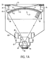
- FIG. 1A represents an X-ray image intensifier tube which comprises, at the input, a separation sheet 23 with the vacuum formed of a suitable material, for example titanium.
- the separation sheet is followed by an entry window 21.
- the assembly is mounted in a vacuum envelope which further comprises a cylindrical surface 43 with a conical part 45, a terminal anode support 49 and a window outlet tube 20.
- the tube is provided at its inlet with a mounting ring 22 to which the separation sheet 23 is connected as well as a support 24 for the inlet screen 21.
- the photoelectron beams 52 coming from a photocathode 13 form an image on a luminescent layer 46 which is preferably deposited on an output screen 20 formed of a plate of optical fibers.
- the electronic image projected onto the output screen generates an optical image in the layer of luminescent material. This optical image is then used in the usual way to be viewed.
- the entrance window 21 comprises in order an aluminum substrate 10, an absorbent layer 11, a scintillator 12 and a photocathode 13.
- the incident X-rays arrive on the structure through the substrate 10 and electrons e- are emitted by photocathode 13.
- the ray 51 penetrates the photocathode 13 which emits electrons 52.
- the same point 50 can emit rays such as the ray 53 in the direction of the substrate 10.
- the ray 53 is reflected according to the radius 54 and electrons 55 are emitted by the photocathode.
- the same point 50 produces several emissions of electrons 52, 55 and this results in a resolution defect in the tube.
- the rays 53 which are emitted in direction of the substrate are absorbed.
- absorption must occur in a continuous and homogeneous manner over the entire surface of the entry window in order to restore an image of homogeneous quality.
- the absorption must be as high as possible for the wavelength of the light emitted by the scintillator.
- the scintillators can be chosen from the following materials: CsI (Na), NaI (Tl), CsI (Tl), CdWO4, Bi4Ge3O12, CaWO4.
- the wavelength of the light emitted is close to 430 nm.
- the absorbent layer must allow this radiation to be absorbed.
- the material can be chosen from the following materials: TiN, CdS, (Cu, PbI2).
- FIG. 2 represents the reflection rate of a TiN layer deposited on an aluminum substrate for light emitted at 430 nm by a CsI (Na) scintillator. This rate is represented as a function of the thickness of the absorbent layer. It is noted that the reflection rate becomes less than 10% as soon as the TiN layer reaches a thickness of approximately 50 nm.
- FIG. 3 represents the reflection rate of a layer of CdS deposited on an aluminum substrate for a wavelength of 430 nm as a function of the thickness of the layer.
- the thicknesses of CdS can be chosen in substantially the following ranges: 115 nm to 135 nm, 185 nm at 235 nm, greater than 260 nm for a light emission at 430 nm.
- Each scintillator will have a light spectrum centered on its own central wavelength. These light spectra are distributed between substantially 400 nm and substantially 600 nm.
- the thicknesses of CdS layers are therefore to be determined both according to a predetermined admissible value for the reflection rate and according to the central emission wavelength of the scintillator used. Those skilled in the art by preliminary measurements of the reflection rate as a function of the thickness for the wavelength and the material chosen can thus easily choose the thickness according to the tolerated reflection rate.
- FIG. 4 represents an embodiment of the invention which includes an additional layer 19 with a low refractive index placed between the scintillator 12 and the photocathode 13.
- an additional layer 19 with a low refractive index placed between the scintillator 12 and the photocathode 13.
- point 63 can be quite distant from the radial direction coming from point 50 perpendicular to the curved surface of the photocathode, a direction which is substantially the axial direction of the columnar crystals.
- the electrons which come from ray 61 will thus contribute to decrease the resolution of the image of the tube.
- This second cause of a decrease in resolution is corrected using a low index layer 19 having a refractive index lower than that of the scintillator 12, placed between the scintillator 12 and the photocathode 13.
- the radius 60 strikes the surface of this layer at point 64 and undergoes a total reflection along the radius 62.
- the light rays which are substantially distant from the axial direction of the columnar crystals are returned and do not participate in the creation of electrons.
- This layer 19 must have a low absorption so as not to disturb the luminosity.
- the material of this layer can be chosen from the following materials: MgF2, cryolite (Na3AlF6). In the useful wavelength range which is between approximately 400 nm and 600 nm, the refractive index of MgF2 is between 1.33 and 1.37 approximately with an extinction index practically zero. The values are substantially similar for the cryolite.
- This chemical barrier consists of a layer chosen from the following materials: Al2O3, Si3N4, SiO2.
- the photocathode material is generally not very conductive, it is possible to ensure a homogeneous distribution of the electrical potential by placing a conductive layer on the photocathode on the side of the scintillator. This conductive layer must also be transparent to allow pass the radiation emitted by the scintillator. If a chemical barrier exists, the conductive and transparent layer is placed between the photocathode and the chemical barrier.
- the following materials can be used: palladium, aluminum, In2O3, SnO2 or the ITO material which a mixture of In2O3 (90%) and SnO2 (10%).
- the entry window produced with an absorbent layer, for example made of TiN, and a photocathode with a high photoelectric efficiency, for example made of K2CsSb, will generally be able to have a photoelectric yield higher than an entry window made without these materials.
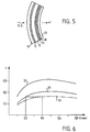
- FIG. 6 represents the variations in the photoelectric efficiency Y of a photocathode as a function of the thickness of the scintillator.
- the thickness of the photocathode is such that the photoelectric efficiency is at its maximum.
- Curve 31 relates to the Al / TiN / CsI, Na / Al2O3 / K2CsSb structure. Its reflection rate of light emitted by the scintillator and reflected by the substrate is less than 10%.
- Curve 32 relates to the Al / CsI, Na / Al2O3 / K2CsSb structure. Its reflection rate is around 70%. Curve 31 is below curve 32 because indeed, the absorbed light is lost and does not can generate electrons.
- Curve 33 relates to the Al / CsI, Na / Cs3Sb structure. Curve 31 is located above curve 33. This means that an entrance window with an absorbent layer and a photocathode with high photoelectric efficiency can exhibit increased performance compared to a usual structure. Likewise, it can be seen that an input window corresponding to curve 31 can have performances equal to those obtained with an input window corresponding to curve 33, and this with a much smaller scintillator thickness.
- this thickness can be reduced from 0.4 to 0.2 mm approximately.
- This reduction in the thickness of the scintillator also contributes to improving the resolution of the tube.
- the crystals which constitute the scintillator generally have, over a certain thickness (ten micrometers), dislocations which cause a diffusion of light.
- the proposed thickness reduction retains a sufficient scintillator thickness so that this dislocated zone only slightly disturbs the mechanisms.
- this reduction in thickness is very advantageous since these X-ray detection tubes require crystals to grow on entry window surfaces of several square decimetres. Such a reduction in thickness results in a significant saving of material and an increased manufacturing yield.
Landscapes
- Image-Pickup Tubes, Image-Amplification Tubes, And Storage Tubes (AREA)
Claims (11)
- Röntgenbildverstärkerröhre mit einem Eintrittsfenster, das mit einem Aluminiumsubstrat versehen ist, das einen Szintillator trägt, der die Röntgenstrahlung, die den Szintillator durch das Substrat hindurch erreicht, in eine sichtbare Lichtstrahlung oder nahezu sichtbare Lichtstrahlung umwandelt, wobei die Lichtstrahlung von einer Fotokathode in einen Elektronenfluß umgesetzt wird, der mit optoelektronischen Mitteln ein sichtbares Bild auf einem Ausgangsschirm liefert, und daß zwischen dem Aluminiumsubstrat und dem Szintillator eine Schicht angeordnet ist, die die Lichtstrahlung aus dem Szintillator in Richtung auf das Aluminiumsubstrat absorbiert, dadurch gekennzeichnet, daß die absorbierende Schicht einen Werkstoff enthält, der aus folgenden Werkstoffen gewählt ist: Titannitrid, Kadmiumschwefel, (Cu, PbI₂).
- Röhre nach Anspruch 1, dadurch gekennzeichnet, daß eine Schicht mit niedrigem Brechungsindex einen Brechungsindex besitzt, der niedriger ist als der der Fotokathode, und diese Schicht ist zwischem dem Szintillator und der Fotokathode angeordnet.
- Röhre nach Anspruch 2, dadurch gekennzeichnet, daß der Werkstoff der Schicht mit niedrigem Brechnungsindex aus folgenden Werkstoffen gewählt ist: MgF₂, Kryolith (Na₃AlF₆).
- Röhre nach einem der Ansprüche 1 bis 3, dadurch gekennzeichnet, daß die Titannitridschicht eine Dicke von wenigstens 50 nm hat.
- Röhre nach Anspruch 4, dadurch gekennzeichnet, daß die Dicke zwischen 75 nm und 120 nm liegt.
- Röhre nach einem der Ansprüche 1 bis 3, dadurch gekennzeichnet, daß die Kadmiumschwefelschicht eine Dicke in einem der folgenden Bereiche hat: zwischen etwa 115 nm und 135 nm, zwischen etwa 185 nm und 235 nm, über etwa 260 nm.
- Röhre nach einem der Ansprüche 1 bis 6, dadurch gekennzeichnet, daß die Fotokathode aus folgenden Werkstoffen gewählt ist: K₂CsSb, Rb₂CsSb, CbCs₃, (SbNa₂K, Cs).
- Röhre nach einem der Ansprüche 1 bis 7, dadurch gekennzeichnet, daß der Szintillator aus folgenden Werkstoffen gewählt wird: CsI(Na), NaI(Tl), CsI(Tl), CdWO₄, Bi₄Ge₃O₁₂, CaWO₄.
- Röhre nach Anspruch 8, dadurch gekennzeichnet, daß der Szintillator aus CsI(Na) eine Dicke hat, die etwa zwischen 100 und 1000 Mikrometer liegt.
- Röhre nach Anspruch 7 und 9, dadurch gekennzeichnet, daß eine chemische Barriere zwischen dem Szintillator und der Fotokathode angeordnet ist, wobei die chemische Barriere aus folgenden Werkstoffen gewählt wird: Al₂O3, Si₃N₄, SiO₂.
- Röhre nach Anspruch 10, dadurch gekennzeichnet, daß eine elektrisch leitende und optisch transparente Schicht zwischen der Fotokathode und der chemischen Barriere angebracht ist, und diese Schicht ist aus folgenden Werkstoffen gewählt wird: Palladium, Aluminium, In₂O3, SnO₂, Mischung von In₂O₃ (90%) und von SnO₂ (10%).
Applications Claiming Priority (2)
| Application Number | Priority Date | Filing Date | Title |
|---|---|---|---|
| FR8716252 | 1987-11-24 | ||
| FR8716252A FR2623659B1 (fr) | 1987-11-24 | 1987-11-24 | Tube intensificateur d'images a rayons x |
Publications (2)
| Publication Number | Publication Date |
|---|---|
| EP0319080A1 EP0319080A1 (de) | 1989-06-07 |
| EP0319080B1 true EP0319080B1 (de) | 1993-09-29 |
Family
ID=9357091
Family Applications (1)
| Application Number | Title | Priority Date | Filing Date |
|---|---|---|---|
| EP88202638A Expired - Lifetime EP0319080B1 (de) | 1987-11-24 | 1988-11-23 | Röntgenstrahl-Bildverstärkerröhre |
Country Status (5)
| Country | Link |
|---|---|
| US (1) | US4982136A (de) |
| EP (1) | EP0319080B1 (de) |
| JP (1) | JP2796320B2 (de) |
| DE (1) | DE3884570T2 (de) |
| FR (1) | FR2623659B1 (de) |
Families Citing this family (9)
| Publication number | Priority date | Publication date | Assignee | Title |
|---|---|---|---|---|
| FR2647955B1 (fr) * | 1989-05-30 | 1991-08-16 | Thomson Tubes Electroniques | Ecran d'entree de tube intensificateur d'image radiologique |
| EP0403802B1 (de) * | 1989-06-20 | 1997-04-16 | Kabushiki Kaisha Toshiba | Röntgenbildverstärker und Verfahren zur Herstellung des Eingangsschirmes |
| JPH0810584B2 (ja) * | 1989-11-07 | 1996-01-31 | 株式会社東芝 | X線イメージ管及びその製造方法 |
| JP3297078B2 (ja) * | 1991-05-24 | 2002-07-02 | 株式会社東芝 | X線イメージ管およびその製造方法 |
| FR2683388A1 (fr) * | 1991-10-31 | 1993-05-07 | Thomson Tubes Electroniques | Tube intensificateur d'image radiologique a resolution amelioree. |
| DE4342217C1 (de) * | 1993-12-10 | 1995-03-30 | Siemens Ag | Röntgenbildverstärker und Verfahren zu seiner Herstellung |
| US20030141814A1 (en) * | 2002-01-29 | 2003-07-31 | Leonid Gaber | Light intensifier tube |
| JP5911274B2 (ja) * | 2011-11-28 | 2016-04-27 | キヤノン株式会社 | 放射線検出装置及び放射線撮像システム |
| US11747493B2 (en) | 2020-09-16 | 2023-09-05 | Amir Massoud Dabiran | Multi-purpose high-energy particle sensor array and method of making the same for high-resolution imaging |
Family Cites Families (14)
| Publication number | Priority date | Publication date | Assignee | Title |
|---|---|---|---|---|
| US2681868A (en) * | 1949-08-10 | 1954-06-22 | Westinghouse Electric Corp | Image amplifier |
| BE500727A (de) * | 1950-01-20 | |||
| US3693018A (en) * | 1966-12-27 | 1972-09-19 | Varian Associates | X-ray image intensifier tubes having the photo-cathode formed directly on the pick-up screen |
| US3706885A (en) * | 1971-01-29 | 1972-12-19 | Gen Electric | Photocathode-phosphor imaging system for x-ray camera tubes |
| DE2134762B2 (de) * | 1971-07-12 | 1977-12-01 | Siemens AG, 1000 Berlin und 8000 München | Fotokathode |
| DE2307026C2 (de) * | 1973-02-13 | 1983-01-20 | Siemens AG, 1000 Berlin und 8000 München | Röntgenbildverstärker-Eingangsschirm |
| JPS5026468A (de) * | 1973-07-09 | 1975-03-19 | ||
| JPS586260B2 (ja) * | 1976-08-30 | 1983-02-03 | 株式会社東芝 | X線螢光増倍管およびその製造方法 |
| JPS5317266A (en) * | 1976-07-31 | 1978-02-17 | Toshiba Corp | X-ray video multiplying tube and its production |
| JPS53122356A (en) * | 1977-04-01 | 1978-10-25 | Hitachi Ltd | X-ray fluorescent film |
| JPS597679B2 (ja) * | 1979-03-28 | 1984-02-20 | 株式会社日立製作所 | シンチレ−タ用結晶及びその製造方法 |
| US4447721A (en) * | 1979-08-31 | 1984-05-08 | Diagnostic Information, Inc. | Panel type X-ray image intensifier tube and radiographic camera system |
| JPS56165251A (en) * | 1980-05-23 | 1981-12-18 | Toshiba Corp | Input surface of x-ray image intensifier and its manufacturing method |
| DE3774746D1 (de) * | 1986-04-04 | 1992-01-09 | Toshiba Kawasaki Kk | Roentgenstrahlenbildverstaerker. |
-
1987
- 1987-11-24 FR FR8716252A patent/FR2623659B1/fr not_active Expired - Lifetime
-
1988
- 1988-11-21 JP JP63292532A patent/JP2796320B2/ja not_active Expired - Lifetime
- 1988-11-21 US US07/274,530 patent/US4982136A/en not_active Expired - Fee Related
- 1988-11-23 DE DE88202638T patent/DE3884570T2/de not_active Expired - Fee Related
- 1988-11-23 EP EP88202638A patent/EP0319080B1/de not_active Expired - Lifetime
Also Published As
| Publication number | Publication date |
|---|---|
| JP2796320B2 (ja) | 1998-09-10 |
| DE3884570T2 (de) | 1994-04-07 |
| EP0319080A1 (de) | 1989-06-07 |
| US4982136A (en) | 1991-01-01 |
| FR2623659B1 (fr) | 1990-03-09 |
| DE3884570D1 (de) | 1993-11-04 |
| FR2623659A1 (fr) | 1989-05-26 |
| JPH01166442A (ja) | 1989-06-30 |
Similar Documents
| Publication | Publication Date | Title |
|---|---|---|
| JP2003521671A (ja) | 放射線検出用複合ナノ発光体スクリーン | |
| FR2831671A1 (fr) | Detecteur de rayonnement x a l'etat solide | |
| EP0186225A1 (de) | Bilddetektor für eine Kamera mit "Tag-Nacht"-Arbeitsweise | |
| FR2687007A1 (fr) | Tube intensificateur d'image notamment du type a focalisation de proximite. | |
| EP0319080A1 (de) | Röntgenstrahl-Bildverstärkerröhre | |
| EP0428667B1 (de) | Eingangsschirm für eine röntgenbildverstärkerröhre | |
| FR2492159A1 (fr) | Ecran convertisseur de neutrons, intensificateur d'images comprenant un tel ecran | |
| US20020134937A1 (en) | Scintillator for electron microscope and method of making | |
| EP0553578B1 (de) | Bildverstärkerröhre mit Intensitätsverteilungkompensation | |
| EP0062553B1 (de) | Treffelektrode für Bildverstärkerröhre und mit solcher Treffelektrode versehene Bildverstärkerröhre mit Video-Ausgang | |
| EP0056671B1 (de) | Photoelektrische Detektorvorrichtung | |
| EP0013241B1 (de) | Röntgenbildverstärkerröhre mit Video-Ausgabe und radiologische Anordnung mit einer derartigen Röhre | |
| EP0983521A1 (de) | Verfahren und vorrichtung zur messung der relativen proportion von uran und plutonium | |
| EP0412887B1 (de) | Mit hohem Wirkungsgrad kathodolumineszenter Schirm für hochleuchtende Kathodenstrahlröhre | |
| FR2545271A1 (fr) | Dispositif de production d'images presentant un rendement quantique ameliore et son procede de fabrication | |
| EP0324676B1 (de) | Verfahren zum Herstellen einer Photokathode für einen Bildverstärker | |
| EP0240951B1 (de) | Röntgenstrahlenbildverstärker | |
| FR2530368A1 (fr) | Ecran scintillateur convertisseur de rayonnement | |
| FR2555321A1 (fr) | Dispositif de detection de rayonnements x a scintillation | |
| EP0079651B1 (de) | Photoelektrischer Detektor | |
| NL8101302A (nl) | Beeldomzetbuis met verbeterd contrast. | |
| EP0851455A1 (de) | Röntgenbildverstärkerröhre | |
| EP0182405A1 (de) | Photoelektrische Vorrichtung zum Nachweisen leuchtender Ereignisse | |
| EP0143714B1 (de) | Lumineszenter Schirm und Verfahren zur Herstellung desselben | |
| JPH08306328A (ja) | X線撮像管 |
Legal Events
| Date | Code | Title | Description |
|---|---|---|---|
| PUAI | Public reference made under article 153(3) epc to a published international application that has entered the european phase |
Free format text: ORIGINAL CODE: 0009012 |
|
| AK | Designated contracting states |
Kind code of ref document: A1 Designated state(s): DE FR GB NL |
|
| 17P | Request for examination filed |
Effective date: 19891129 |
|
| RAP1 | Party data changed (applicant data changed or rights of an application transferred) |
Owner name: N.V. PHILIPS' GLOEILAMPENFABRIEKEN Owner name: LABORATOIRES D'ELECTRONIQUE PHILIPS |
|
| 17Q | First examination report despatched |
Effective date: 19911111 |
|
| GRAA | (expected) grant |
Free format text: ORIGINAL CODE: 0009210 |
|
| AK | Designated contracting states |
Kind code of ref document: B1 Designated state(s): DE FR GB NL |
|
| PG25 | Lapsed in a contracting state [announced via postgrant information from national office to epo] |
Ref country code: NL Effective date: 19930929 |
|
| REF | Corresponds to: |
Ref document number: 3884570 Country of ref document: DE Date of ref document: 19931104 |
|
| GBT | Gb: translation of ep patent filed (gb section 77(6)(a)/1977) |
Effective date: 19931223 |
|
| NLV1 | Nl: lapsed or annulled due to failure to fulfill the requirements of art. 29p and 29m of the patents act | ||
| PLBE | No opposition filed within time limit |
Free format text: ORIGINAL CODE: 0009261 |
|
| STAA | Information on the status of an ep patent application or granted ep patent |
Free format text: STATUS: NO OPPOSITION FILED WITHIN TIME LIMIT |
|
| 26N | No opposition filed | ||
| REG | Reference to a national code |
Ref country code: FR Ref legal event code: CJ Ref country code: FR Ref legal event code: CD |
|
| REG | Reference to a national code |
Ref country code: FR Ref legal event code: TP |
|
| PGFP | Annual fee paid to national office [announced via postgrant information from national office to epo] |
Ref country code: FR Payment date: 20001121 Year of fee payment: 13 |
|
| PGFP | Annual fee paid to national office [announced via postgrant information from national office to epo] |
Ref country code: GB Payment date: 20001129 Year of fee payment: 13 |
|
| PGFP | Annual fee paid to national office [announced via postgrant information from national office to epo] |
Ref country code: DE Payment date: 20010118 Year of fee payment: 13 |
|
| PG25 | Lapsed in a contracting state [announced via postgrant information from national office to epo] |
Ref country code: GB Free format text: LAPSE BECAUSE OF NON-PAYMENT OF DUE FEES Effective date: 20011123 |
|
| REG | Reference to a national code |
Ref country code: GB Ref legal event code: IF02 |
|
| PG25 | Lapsed in a contracting state [announced via postgrant information from national office to epo] |
Ref country code: DE Free format text: LAPSE BECAUSE OF NON-PAYMENT OF DUE FEES Effective date: 20020702 |
|
| GBPC | Gb: european patent ceased through non-payment of renewal fee |
Effective date: 20011123 |
|
| PG25 | Lapsed in a contracting state [announced via postgrant information from national office to epo] |
Ref country code: FR Free format text: LAPSE BECAUSE OF NON-PAYMENT OF DUE FEES Effective date: 20020730 |
|
| REG | Reference to a national code |
Ref country code: FR Ref legal event code: ST |
|
| REG | Reference to a national code |
Ref country code: FR Ref legal event code: ST |