EP0319098A2 - Formation d'épreuves par un procédé électrostatique utilisant la séparation des couleurs d'un négatif - Google Patents
Formation d'épreuves par un procédé électrostatique utilisant la séparation des couleurs d'un négatif Download PDFInfo
- Publication number
- EP0319098A2 EP0319098A2 EP88202715A EP88202715A EP0319098A2 EP 0319098 A2 EP0319098 A2 EP 0319098A2 EP 88202715 A EP88202715 A EP 88202715A EP 88202715 A EP88202715 A EP 88202715A EP 0319098 A2 EP0319098 A2 EP 0319098A2
- Authority
- EP
- European Patent Office
- Prior art keywords
- photoconductor
- polarity
- background
- charges
- color
- Prior art date
- Legal status (The legal status is an assumption and is not a legal conclusion. Google has not performed a legal analysis and makes no representation as to the accuracy of the status listed.)
- Granted
Links
Images

Classifications
-
- G—PHYSICS
- G03—PHOTOGRAPHY; CINEMATOGRAPHY; ANALOGOUS TECHNIQUES USING WAVES OTHER THAN OPTICAL WAVES; ELECTROGRAPHY; HOLOGRAPHY
- G03G—ELECTROGRAPHY; ELECTROPHOTOGRAPHY; MAGNETOGRAPHY
- G03G13/00—Electrographic processes using a charge pattern
- G03G13/01—Electrographic processes using a charge pattern for multicoloured copies
Definitions
- the invention relates to an electrophotographic image reversal process for the production of positive color imagery from negative color separation films and finds an application in the production of color pre-press proofs.
- pre-press proofs The purpose of pre-press proofs is to enable one to assess the color balance, registration, appearance, among other features, which can be expected from the press run and to correct the separation films before the printing plates are made therefrom. It is also desirable to produce so-called "customer proofs" which tell the customer how the original artwork will appear when printed with plates made from the separation films. Thus, it is essential that the pre-press proof have the same appearance as the press print. Accordingly, in addition to matching the color balance of the press print, the customer proof should be on the same paper as the press print.
- the separation film can be a positive film or a negative film, depending on the type of printing plate to be used.
- the printing plate used can be the so-called positive working and negative working lithographic or offset printing plate as is known in this field.
- a positive working plate is exposed to light through a film positive on which the information to be printed corresponds to opaque areas and the non-printing background areas correspond to transparent areas.
- the exposed areas on the plate are rendered removable by chemical treatment and the underlying plate surface, usually grained aluminum, forms the water receptive non-printing or non-image areas, whereas the unexposed areas form the ink receptive printing image areas.
- a negative working printing plate is exposed to light through a film negative on which the information to be printed corresponds to transparent areas and the non-printing background areas correspond to opaque areas. In this case, the exposed areas on the plate become photo-hardened and form the ink receptive printing areas, whereas the unexposed areas are removed by chemical treatment and the underlying water receptive plate surface forms the non-printing or non-image areas.
- pre-press proofs containing in general four colors, such as yellow, magenta, cyan and black.
- Such pre-press proofing processes are disclosed, for example, in United States Patent Nos. 3,809,555 and 3,862,848.
- An apparatus for the production of electrophotographic pre-press proofs is described, for example, in United States Patents Nos. 4,556,309 and 4,557,583.
- electrophotographic pre-press proofs can be produced by charging a photoconductive recording member, followed by exposure through a separation film positive corresponding to one color, followed by toning of the exposed photoconductor with a liquid dispersed toner of the appropriate color, followed by in-register transfer of the color toned image deposit directly or through an intermediate or offset member to a receptor, such as paper, usually of the same grade as the printing stock. These process steps are then repeated with separation film positives of the other three or more colors and appropriate color toners to produce a muticolor proof.
- the receptor paper After all of the required color toner deposits have been transferred to the receptor paper, it is coated by spraying or other methods with a clear polymer layer to transparentize the color toner deposits and fuse them to the receptor paper sheet.
- United States Patent No. 3,300,410 discloses a photoconductive recording member that consists of a sheet of paper that is coated with photoconductive zinc oxide and charged to negative polarity. The sheet is exposed through a negative film and toned with a positive liquid toner having film forming colloidal size conductive resin particles to form, after evaporation of the carrier liquid of such toner and drying, a permanently fixed conductive and colorless film deposit in the unexposed or non-image areas. The sheet was then re-charged negatively and only image areas free of conductive colorless film deposit accepted charges. These areas were then toned with a colored positive toner to form visible image deposits, whereby a reversal image or a positive reproduction of the negative film was obtained.
- the conductive deposit affixed in the non-image areas had a low tinting strength, it did not affect the appearance of the photoconductor.
- the low tinting strength materials used were alumina hydrate, magnesium and barium carbonates, talc, plaster of Paris, conductive zinc oxide, mica and silica, having a refractive index less than about 1.6 or 1.7 and an electrical volume resistivity less than about 109 ohmcm. In each of the above cases, the colorless or low tinting strength toner deposits were conductive and thus did not accept charges.
- This invention provides an image reversal process for the production of electrophotographic color proofs from negative separation films wherein the electrophotoconductive recording member is reusable and wherein the proofs are produced on printing stock paper, very closely matching the appearance of the printed sheet.
- the process of the invention includes exposing an electrophotoconductor that is charged to a first polarity through a color separation negative film which may be in contact therewith, developing the unexposed areas on the photoconductor with opposite polarity background toner to form background deposits thereon in areas corresponding to the opaque non-image or background areas on the negative, subjecting the photoconductor and the background deposits thereon to corona discharge of said first polarity to charge the photoconductor in the areas free of said background deposits, that is, in areas corresponding to the transparent image areas on the negative, removing charges of said first polarity from the background deposits, developing the image areas on the photoconductor with opposite polarity color toner, and transferring the thus formed color toner deposits to a receptor such as printing stock paper.
- the charges Prior to development with the color toner, the charges are removed from the background deposits to ensure that no color toner will be attracted thereto, since any color toner contained on the background deposits would transfer onto the receptor and form thereon objectionable fog in the non-image or background areas.
- the background deposits are not adhesively affixed to the photoconductor, yet do not transfer to the receptor but can be easily removed from the photoconductor when desired.
- the process is repeated to transfer of the additional specific color developed image in proper registry.
- a proper toner for the specific color image will be used.
- particulate materials of the type disclosed in United Kingdom Patent No. 998,599 referred to above are not truly conductive, per se, and if incorporated in toner compositions as hereinafter described, are useful for making background toners in accordance with this invention to form background deposits which differ very significantly from the low tinting strength toners of United Kingdom Patent No. 998,599.
- the background deposits formed in accordance with this invention : - are non-conductive and are thus chargeable, yet easily dischargeable; - are not adhesively affixed to the photoconductor; - are substantially not transferable; and - can be easily cleaned off the photoconductor to render it reusable.
- particulate material such as calcium carbonate, micronic size celluloses such as methyl cellulose and carboxy methyl cellulose, polymeric materials such as polyvinyl pyrollidone, polyvinyl alcohol and calcium resinate, carbohydrates such as starch and dextrin, silicates such as bentonite, asbestine and montmorillonite, clays such as kaolin and attapulgus clay and the like, as well as dielectric or highly insulative polymeric materials in particulate form, which are insoluble in the carrier liquid, such as epoxies, acrylics, polyvinyl chloride, polyvinyl acetate, polyvinyl butyral, polyesters, polystyrene, polyethylene and the like.Mixtures of these materials can also be used.
- the background toner of this invention is prepared by dispersing particulate materials of the above disclosed type in the toner carrier liquid such as isoparaffinic hydrocarbon in the presence of a soluble dispersing aid or wetting agent such as acrylic polymer, rosin ester and the like.
- a charge director or polarity control agent can be included in the dispersion.
- the proportion of such dispersing aid is kept at a minimum, such as not more than about 25 percent by weight of the particulate material.
- no transfer enhancing materials such as waxes or lattice forming substances are included in the background toners of this invention.
- the background deposits formed by the above disclosed background toners of this invention remain, upon drying, on the photoconductor surface due to the presence of the small proportion of the soluble dispersing aid, without becoming affixed thereto. Therefore, they can be applied to reusable photoconductors and can be very easily removed therefrom when desired.
- background deposits are not affixed to the photoconductor, they are electrostatically substantially not transferable, at least not at transfer voltages normally used in the process for the color toners. At higher voltages some random transfer of the background deposit may occur, without, however, affecting the appearance of the receptor.This is because the above disclosed particulate materials become fully transparent when the aforementioned clear polymer film is formed on the receptor.
- a further essential requirement of the background deposit of this invention is that its capacitance must be substantially lower than that of the photoconductor. This is accomplished by the above disclosed toner composition, wherein the proportion of the dispersing aid is insufficient not only to affix the toner deposit to the photoconductor but also to cement together the individual toner particles and thereby to form a continuous layer.
- the deposit is discontinuous, in that it comprises substantially discrete weakly coherent particles having voids or air pockets therebetween.
- the capacitance of a background deposit layer having such a structure irrespective of the layer thickness and of the dielectric constant of the materials contained therein, is per se lower than the capacitance of the commonly known continuous layer photoconductors.
- the background deposit of this invention can be charged positively and negatively.
- the rate of decay of the charge accepted by the background deposit is, due to its low capacitance, significantly faster than the rate of dark decay of the charge accepted by the photoconductor.
- both the background deposit and the photoconductor are charged to one polarity, application of weak charges of opposite polarity will readily discharge the background deposit, due to its low capacitance and consequently low surface charge density, without significantly affecting the charge on the photoconductor.
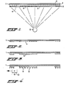
- a photoconductor is designated generally by reference numeral 1.
- the photoconductor 1 includes a photoconductive layer 2 that is secured to a conductive substrate 3.
- the photoconductor 1 is uniformly charged to a negative polarity as indicated by negative charges 4.
- a first color negative separation film 5, containing opaque non-image or background areas 6 and transparent image areas 7, is placed in contact with the photoconductor 1 for contact exposure through a light source 8.
- Fig. 2 illustrates the photoconductor 1 after exposure by the light source 8.
- the photoconductor 1 retains the negative electrostatic charges 4 only in the areas corresponding to the opaque background areas 6 of the negative film 5 illustrated in Fig. 1.
- the photoconductor 1 is then toned with a positive background toner of the invention which forms background toner deposits 9, as illustrated in Fig. 3.
- Fig. 4 illustrates the step where the photoconductor 1 and the background deposits 9 are charged positively by means of a corona generator 10. Only the background deposits 9 accept positive charges 11, while the n-type photoconductor 1 remains uncharged. It is to be noted that this is an optional step that can be used to reduce the negative charge which would be accepted by the background deposits 9 in the following step illustrated in the next Figure.
- Fig. 5 illustrates the step where the photoconductor 1 and the background deposits 9 are charged negatively.
- the negative charges 4 on the photoconductor 1 are of the same magnitude as in FIG. 1 that is needed for toner attraction.
- the magnitude of negative charges 12 on the background deposits 9 depends on whether or not the optional step illustrated in FIG. 4 has been carried out. Namely, if the background deposits 9 carry the positive charges 11 induced in the preceding optional step, the positive charges on the background deposits 9 at first have to be neutralized by this step of negative charging before the background deposits 9 can be actually charged negatively. In this case, the magnitude of negative charges induced in this step on the background deposits 9 would be considerably lower than in the case where the optional step is omitted.
- Fig. 6 illustrates the step where the photoconductor 1 and the background deposits 9 are again charged positively.
- the positive charging current is selected to be low enough so as not to appreciably affect the negative charges on the high capacitance photoconductor 1, yet sufficient to substantially neutralize the negative charges 12 on the background deposits 9. This is possible due to the low capacitance and consequently, low surface charge density, of the background deposits 9.
- the optional step illustrated in Fig. 4 is performed, positive charges will be induced in the background deposits 9 to actually repel positive color toner therefrom in the following step of toning.
- the photoconductor 1 is then toned with a positive toner of a first color to form first color toner deposits 13 thereon, as illustrated in Fig. 7. Accordingly, no color toner is attracted to the background deposits 9.
- Fig. 8 illustrates a receptor 14, such as paper, after electrostatic transfer of the first color image deposits 13 from the photoconductor 1 of Fig. 7 has taken place.
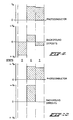
- Figs. 9 and 10 illustrate the effects of charging in the steps described in Figs. 4, 5, and 6 corresponding to process steps 5, 6, and 7 respectively.
- the charging effects are illustrated in terms of the surface voltages Vs corresponding to the surface charges.
- Fig. 9 illustrates the effect of the positive Vs induced on the background deposits 9 in optional step 5.
- step 6 the photoconductor 1 is charged negatively to the top Vs, while the negative Vs induced on the background deposits 9 is relatively low. Consequently, at very low positive charging current in step 7, the negative Vs on the background deposits 9 is reduced to zero, or even a positive Vs is induced thereon, as shown by the dotted lines in Fig. 9, while the negative top Vs on the photoconductor 1 remains virtually unaffected.
- step 5 is omitted, as illustrated in Fig. 10, the negative Vs induced on the background deposits 9 in step 6 is high. In this case a higher current is needed for positive charging in step 7 to reduce the negative Vs on the background deposits 9 to zero. At the same time, this results in a greater drop in the top Vs on the photoconductor.
- Reusable photoconductors which are suitable for a colorproofing process in accordance with this invention can be, for example, crystalline sputtered cadmium sulfide as disclosed, for example, in United States Patent No. 4,025,339. Other reusable photoconductors can be used if so desired.
- the colorproofing process of this invention can be conveniently carried out in electrophotographic color proofing equipment as described, for example, in United States Patents Nos. 4,556,309 and 4,557,583, which were referred to above and which were operated with the above referred to crystalline cadmium sulfide photoconductor on a stainless steel substrate to prepare the data for the illustrative examples given further below.
- electrostatic transfer is effected by means of rollers and the toner deposits are transferred from the photoconductor first to an offset or intermediate member and then to the receptor proof paper.
- an offset or intermediate member For simplicity, however, in the following examples reference is made only to a single transfer from the photoconductor to a paper receptor. It is to be noted that double transfer through an offset or intermediate member is equally applicable as well as electrostatic transfer by other means, such as, for example, by corona discharge.
- Liquid toner compositions forming electrostatically transferable color deposits useful in the colorproofing process of this invention are disclosed, for example, in United States Patent No. 3,419,411 and in co-pending U.S. Patent Application entitled “Method Of Image Fixing In Color Electrostatography", Serial No. 920,510, filed October 17, 1986 and owned by the same assignee as this application. These are incorporated herein by reference.
- the background toner in this and the following examples included a dispersion of pigment grade calcium carbonate and about 20 percent by weight acrylic dispersing aid in isoparaffinic hydrocarbon carrier liquid.
- the densities of the colors on the proof had to be within ⁇ 0.05 tolerance as follows: black - 1.80 yellow - 0.90 magenta - 1.45 cyan - 1.35, at 0.00 fog density in the background areas. All densities were measured with a Macbeth 927 wide band reflection densitometer.
- the following voltages were used throughout: for black - 500V, for yellow - 900V, for magenta and cyan -1500V. At these voltages there was no appreciable transfer of the background deposits 9 to the art paper.
- the time lapse between negatively charging the photoconductor 1 and commencement of background toning is about 100 seconds. Also, the time lapse between negative charging in step 6 and commencement of color toning is about 100 seconds, and the charges or surface voltages on the photoconductor 1 and on the background deposits 9 at such time determine the density which the color toners develop during the following toning step.
- the photoconductor was charged negatively for background toning and then in step 6 for color toning with a corona current of 350 microamps. This induced a top surface voltage on the photoconductor 1 of 30V, which in 100 seconds decayed to 28V.
- step 6 the negative charging in step 6 induced on the background deposits 9 a surface voltage of 50V, which in 100 seconds decayed to 20V.
- step 5 the photoconductor 1 and the background deposits 9 were charged positively with 200 microamps corona current.This induced a positive surface voltage of about 50V on the background deposits 9.
- Step 6 of negative charging immediately followed step 5.
- the negative surface voltage induced on the background deposits 9 was only about 30V.
- the photoconductor 1 and the background deposits 9 were charged positively with a corona current of 50 microamps, which reduced the negative voltage on the background deposits 9 to zero.
- the top surface voltage on the photoconductor 1 was reduced by only 1V to 29V, which in 100 seconds decayed to 27V.
- Example 2 was repeated with the exception that in step 7 the positive corona current was 60 microamps. This induced a positive voltage on the background deposits 9 of 12V, which in 100 seconds decayed to 5V. The top surface voltage on the photoconductor 1 was reduced by 2V to 28V, which in 100 seconds decayed to 26V.
- step 7 the positive corona current had to be 75 microamps to reduce the negative charge on the background deposits 9 to zero. However, this reduced the top negative surface voltage on the photoconductor 1 to 26V, which in 100 seconds decayed to 24V.
Landscapes
- Physics & Mathematics (AREA)
- General Physics & Mathematics (AREA)
- Color Electrophotography (AREA)
- Wet Developing In Electrophotography (AREA)
- Separation Of Suspended Particles By Flocculating Agents (AREA)
- Developing Agents For Electrophotography (AREA)
Priority Applications (1)
| Application Number | Priority Date | Filing Date | Title |
|---|---|---|---|
| AT88202715T ATE92649T1 (de) | 1987-12-01 | 1988-11-28 | Elektrostatische herstellung von abzuegen durch farbentrennung eines negatives. |
Applications Claiming Priority (2)
| Application Number | Priority Date | Filing Date | Title |
|---|---|---|---|
| AU5694/87 | 1987-12-01 | ||
| AUPI569487 | 1987-12-01 |
Publications (3)
| Publication Number | Publication Date |
|---|---|
| EP0319098A2 true EP0319098A2 (fr) | 1989-06-07 |
| EP0319098A3 EP0319098A3 (en) | 1990-09-12 |
| EP0319098B1 EP0319098B1 (fr) | 1993-08-04 |
Family
ID=3772611
Family Applications (1)
| Application Number | Title | Priority Date | Filing Date |
|---|---|---|---|
| EP88202715A Expired - Lifetime EP0319098B1 (fr) | 1987-12-01 | 1988-11-28 | Formation d'épreuves par un procédé électrostatique utilisant la séparation des couleurs d'un négatif |
Country Status (6)
| Country | Link |
|---|---|
| US (1) | US5055365A (fr) |
| EP (1) | EP0319098B1 (fr) |
| JP (1) | JPH0242463A (fr) |
| AT (1) | ATE92649T1 (fr) |
| CA (1) | CA1323653C (fr) |
| DE (1) | DE3882928T2 (fr) |
Families Citing this family (1)
| Publication number | Priority date | Publication date | Assignee | Title |
|---|---|---|---|---|
| JP6380059B2 (ja) * | 2014-12-01 | 2018-08-29 | セイコーエプソン株式会社 | 色調整装置、色調整方法、および印刷システム |
Family Cites Families (5)
| Publication number | Priority date | Publication date | Assignee | Title |
|---|---|---|---|---|
| DE1141180B (de) * | 1958-01-13 | 1962-12-13 | Commonwealth von Australien, Melbourne (Australien) | Verfahren zur Bildherstellung in der Xerografie |
| US4556309A (en) * | 1982-12-29 | 1985-12-03 | Coulter Systems Corporation | Electrophotographic imaging apparatus, particularly for color proofing and method |
| US4764443A (en) * | 1985-10-31 | 1988-08-16 | Stork Research B.V. | Method of image reversal in color electrophotography |
| EP0225456B1 (fr) * | 1985-10-31 | 1990-08-16 | Stork Colorproofing B.V. | Procédé d'inversion d'images en l'électrophotographie à couleurs |
| US4804602A (en) * | 1986-03-12 | 1989-02-14 | Eastman Kodak Company | Method and apparatus utilizing corona erase for improving a multi-color electrophotographic image |
-
1988
- 1988-11-28 US US07/276,771 patent/US5055365A/en not_active Expired - Fee Related
- 1988-11-28 DE DE88202715T patent/DE3882928T2/de not_active Expired - Fee Related
- 1988-11-28 AT AT88202715T patent/ATE92649T1/de not_active IP Right Cessation
- 1988-11-28 EP EP88202715A patent/EP0319098B1/fr not_active Expired - Lifetime
- 1988-11-30 CA CA000584541A patent/CA1323653C/fr not_active Expired - Fee Related
- 1988-12-01 JP JP63305848A patent/JPH0242463A/ja active Granted
Also Published As
| Publication number | Publication date |
|---|---|
| JPH0242463A (ja) | 1990-02-13 |
| JPH0465377B2 (fr) | 1992-10-19 |
| EP0319098A3 (en) | 1990-09-12 |
| CA1323653C (fr) | 1993-10-26 |
| ATE92649T1 (de) | 1993-08-15 |
| US5055365A (en) | 1991-10-08 |
| DE3882928D1 (de) | 1993-09-09 |
| DE3882928T2 (de) | 1994-02-03 |
| EP0319098B1 (fr) | 1993-08-04 |
Similar Documents
| Publication | Publication Date | Title |
|---|---|---|
| EP0424093B1 (fr) | Méthodes et appareils de formation d'images | |
| US3574614A (en) | Process of preparing multiple copies from a xeroprinting master | |
| CA1332117C (fr) | Systeme d'imagerie | |
| EP0636948B1 (fr) | Procédé et dispositif pour appliquer une couche adhésive pour le transfert d'images amélioré dans l'électrophotographie | |
| DE69010638T2 (de) | Xerodruckverfahren. | |
| CA1332118C (fr) | Systeme d'imagerie | |
| US4255508A (en) | Flexible metal printing cylinder having a coating of crystalline photoconductive material | |
| EP0319098B1 (fr) | Formation d'épreuves par un procédé électrostatique utilisant la séparation des couleurs d'un négatif | |
| US4835570A (en) | Apparatus for printing fixed and variable indicia | |
| US4986211A (en) | Toning method and member for electrostatography | |
| US5194351A (en) | Single pass digital xerographic process color reproduction | |
| US4764443A (en) | Method of image reversal in color electrophotography | |
| EP0226750B1 (fr) | Procédé de la formation d'images à couleurs électrostatique par inversion d'images | |
| AU598702B2 (en) | Electrostatic proofing of negative color separations | |
| EP0225456B1 (fr) | Procédé d'inversion d'images en l'électrophotographie à couleurs | |
| US4007041A (en) | Electrophotographic printing method | |
| US3787206A (en) | Photoelectricphoretic imaging method including at least one electrode carrying a pattern | |
| US3748126A (en) | Multiple copy selective re wetting printing | |
| US5021313A (en) | Image reversal process | |
| US5030530A (en) | Method of electrostatic color proofing | |
| US4705696A (en) | Method of making a lithographic printing plate, printing plates made by the method, and the use of such printing plates to make lithographic prints | |
| US5162180A (en) | Xeroprinting process using reversal development process | |
| US20030203294A1 (en) | Method for producing developed electrostatic images using multiple toner fountains | |
| US4794063A (en) | Photoreceptor for electrophography, method for the production thereof and method of the image formation thereby | |
| US20030036009A1 (en) | Method for producing developed electrostatic images using multiple toner fountains |
Legal Events
| Date | Code | Title | Description |
|---|---|---|---|
| PUAI | Public reference made under article 153(3) epc to a published international application that has entered the european phase |
Free format text: ORIGINAL CODE: 0009012 |
|
| AK | Designated contracting states |
Kind code of ref document: A2 Designated state(s): AT BE CH DE ES FR GB GR IT LI LU NL SE |
|
| PUAL | Search report despatched |
Free format text: ORIGINAL CODE: 0009013 |
|
| AK | Designated contracting states |
Kind code of ref document: A3 Designated state(s): AT BE CH DE ES FR GB GR IT LI LU NL SE |
|
| 17P | Request for examination filed |
Effective date: 19901024 |
|
| 17Q | First examination report despatched |
Effective date: 19920602 |
|
| RAP1 | Party data changed (applicant data changed or rights of an application transferred) |
Owner name: COULTER CORPORATION |
|
| GRAA | (expected) grant |
Free format text: ORIGINAL CODE: 0009210 |
|
| AK | Designated contracting states |
Kind code of ref document: B1 Designated state(s): AT BE CH DE ES FR GB GR IT LI LU NL SE |
|
| PG25 | Lapsed in a contracting state [announced via postgrant information from national office to epo] |
Ref country code: SE Effective date: 19930804 Ref country code: NL Effective date: 19930804 Ref country code: LI Effective date: 19930804 Ref country code: GR Free format text: LAPSE BECAUSE OF FAILURE TO SUBMIT A TRANSLATION OF THE DESCRIPTION OR TO PAY THE FEE WITHIN THE PRESCRIBED TIME-LIMIT Effective date: 19930804 Ref country code: ES Free format text: THE PATENT HAS BEEN ANNULLED BY A DECISION OF A NATIONAL AUTHORITY Effective date: 19930804 Ref country code: CH Effective date: 19930804 Ref country code: BE Effective date: 19930804 Ref country code: AT Effective date: 19930804 |
|
| REF | Corresponds to: |
Ref document number: 92649 Country of ref document: AT Date of ref document: 19930815 Kind code of ref document: T |
|
| REF | Corresponds to: |
Ref document number: 3882928 Country of ref document: DE Date of ref document: 19930909 |
|
| ET | Fr: translation filed | ||
| ITF | It: translation for a ep patent filed | ||
| REG | Reference to a national code |
Ref country code: CH Ref legal event code: PL |
|
| PG25 | Lapsed in a contracting state [announced via postgrant information from national office to epo] |
Ref country code: LU Free format text: LAPSE BECAUSE OF NON-PAYMENT OF DUE FEES Effective date: 19931130 |
|
| NLV1 | Nl: lapsed or annulled due to failure to fulfill the requirements of art. 29p and 29m of the patents act | ||
| PLBE | No opposition filed within time limit |
Free format text: ORIGINAL CODE: 0009261 |
|
| STAA | Information on the status of an ep patent application or granted ep patent |
Free format text: STATUS: NO OPPOSITION FILED WITHIN TIME LIMIT |
|
| 26N | No opposition filed | ||
| PGFP | Annual fee paid to national office [announced via postgrant information from national office to epo] |
Ref country code: FR Payment date: 19951013 Year of fee payment: 8 |
|
| PGFP | Annual fee paid to national office [announced via postgrant information from national office to epo] |
Ref country code: GB Payment date: 19951026 Year of fee payment: 8 |
|
| PGFP | Annual fee paid to national office [announced via postgrant information from national office to epo] |
Ref country code: DE Payment date: 19951027 Year of fee payment: 8 |
|
| PG25 | Lapsed in a contracting state [announced via postgrant information from national office to epo] |
Ref country code: GB Effective date: 19961128 |
|
| GBPC | Gb: european patent ceased through non-payment of renewal fee |
Effective date: 19961128 |
|
| PG25 | Lapsed in a contracting state [announced via postgrant information from national office to epo] |
Ref country code: FR Effective date: 19970731 |
|
| PG25 | Lapsed in a contracting state [announced via postgrant information from national office to epo] |
Ref country code: DE Effective date: 19970801 |
|
| REG | Reference to a national code |
Ref country code: FR Ref legal event code: ST |
|
| PG25 | Lapsed in a contracting state [announced via postgrant information from national office to epo] |
Ref country code: IT Free format text: LAPSE BECAUSE OF NON-PAYMENT OF DUE FEES;WARNING: LAPSES OF ITALIAN PATENTS WITH EFFECTIVE DATE BEFORE 2007 MAY HAVE OCCURRED AT ANY TIME BEFORE 2007. THE CORRECT EFFECTIVE DATE MAY BE DIFFERENT FROM THE ONE RECORDED. Effective date: 20051128 |