EP0319677A2 - Abtast- und Halteschaltung für Fernmeldeanlagen - Google Patents
Abtast- und Halteschaltung für Fernmeldeanlagen Download PDFInfo
- Publication number
- EP0319677A2 EP0319677A2 EP88117130A EP88117130A EP0319677A2 EP 0319677 A2 EP0319677 A2 EP 0319677A2 EP 88117130 A EP88117130 A EP 88117130A EP 88117130 A EP88117130 A EP 88117130A EP 0319677 A2 EP0319677 A2 EP 0319677A2
- Authority
- EP
- European Patent Office
- Prior art keywords
- output
- capacitor
- sample
- bipolar transistors
- constant current
- Prior art date
- Legal status (The legal status is an assumption and is not a legal conclusion. Google has not performed a legal analysis and makes no representation as to the accuracy of the status listed.)
- Granted
Links
Images
Classifications
-
- G—PHYSICS
- G11—INFORMATION STORAGE
- G11C—STATIC STORES
- G11C27/00—Electric analogue stores, e.g. for storing instantaneous values
- G11C27/02—Sample-and-hold arrangements
- G11C27/024—Sample-and-hold arrangements using a capacitive memory element
- G11C27/026—Sample-and-hold arrangements using a capacitive memory element associated with an amplifier
Definitions
- the invention relates to a sample and hold circuit with a sampling circuit located between an input terminal and a capacitor, the sampling pulses supplied by it allow the capacitor to be charged in accordance with an input signal present at the input terminal and with an output circuit which is provided between the capacitor and an output terminal , from which an output signal corresponding to the signal voltage stored in each case on the capacitor can be emitted.
- Sample and hold circuits of the known type are constructed from transistors and RC elements. The way you work is assumed to be known. For such sample and hold circuits, there may be a requirement that they must be usable for a wide speed range, e.g. B. for sampling rates corresponding to a sampling frequency range between 1 and 500 kHz. This results in the problem that a charging capacitor contained in sample and hold circuits of the type required by the invention must be charged relatively quickly on the one hand at the highest occurring sampling frequency, but that this capacitor always discharges only very slowly when operating at the lowest occurring sampling frequency may. In corresponding known circuit arrangements, relatively high-quality and correspondingly complex components were therefore used to charge the capacitor mentioned, in order in this way to obtain the required charge even at the highest sampling frequencies that occur to ensure the capacitor. Despite this special effort, it has proven to be problematic or even impossible in known cases to achieve the high sampling rate required in each case.
- the object is to design a circuit arrangement of the type specified in such a way that the required charging of the charging capacitor can be achieved with certainty on the one hand with relatively simple means at the highest sampling frequency, but on the other hand this capacitor is only discharged very slowly at the lowest sampling frequency. In any case, a good transient response that is adequate for the sampling frequency should be achieved.
- the invention solves this problem in that the sampling circuit contains a differential amplifier made up of bipolar transistors, to the output of which the capacitor and the output circuit are connected, that the output circuit contains an output amplifier made up of bipolar transistors, and in that both the differential amplifier and Output amplifiers are connected to constant current sources, which are also constructed from bipolar transistors and which are so effectively controlled in response to the occurrence of the scanning pulses that the level of the constant current flowing through them is proportional to the respective scanning pulse frequency.
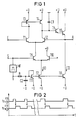
- FIG. 1 shows a circuit-like exemplary embodiment of a sample and hold circuit according to the invention
- 2 shows in a time diagram different pulse-pause ratios with regard to sample and hold pulses.
- the transistors T1, T2, T3 and T4 form a differential amplifier.
- the transistors are bipolar transistors.
- On A charging capacitor C1 is connected to the output.
- An output circuit also connected to its output is formed with the help of transistors T5 and T6. These transistors form an output amplifier with an output terminal A.
- a sampling circuit which consists not only of the transistors T1 to T4 of the differential amplifier but also of further transistors T7, T9, T10, T11.
- the capacitor C1 can be charged by means of sampling pulses supplied via a terminal S, in accordance with the input signal present at the input terminal E.
- a signal voltage stored in each case on the capacitor is output via the output connection A, with the aid of the output circuit consisting of the transistors T5, T6 and T8, which is provided between the charging capacitor C1 and the output connection A.
- transistors T5 and T6 form the output amplifier mentioned.
- Both the differential amplifier formed from the transistors T1 to T4 and the output amplifier consisting of the transistors T5 and T6 are connected to constant current sources. These are formed with the help of transistors T7 and T8. These transistors are also bipolar transistors. These transistors are effectively controlled on the occurrence of the scanning pulses which arrive via the terminal S in accordance with the frequency of their occurrence, in such a way that the level of the constant current flowing through them is proportional to the respective scanning pulse frequency.
- the bipolar transistors T7 and T8, which form the constant current sources mentioned are connected on the input side to the output of a frequency-current converter MF. The scanning pulses from terminal S are fed to its input.
- the frequency-current converter mentioned is implemented as a monostable multivibrator. The same is triggered by the sampling pulses (arriving via S). With the output of this monostable multivibrator is a further capacitor C2 via a resistor R. connected.
- the base connections of the bipolar transistors T7 and T8 of the constant current sources are connected to it.
- a further bipolar transistor T9 is connected, which arrives directly into the conductive one through the scanning pulses (arriving via S) Condition is controllable.
- the output of the output amplifier which is formed from the bipolar transistors T5 and T6, is also connected to the inverting input of the differential amplifier, which is formed from the bipolar transistors T1 to T4.
- the monostable flip-flop MF triggers a pulse of constant width for each scanning pulse (arriving via S). This is shown in FIG 2. (Incoming sampling pulses of different widths are shown in FIG. 2 at ts.)
- the pulse which is respectively passed on via the monostable flip-flop MF and which is passed on via the terminal v and the resistor R is in each case of a constant width.
- the constant current Io that flows across the collector of the bipolar transistor T7 is exactly proportional to the sampling pulse frequency.
- the desired goal has thus been achieved: the larger the constant current I0, the faster the capacitor C1 charges - and this in turn depends on the sampling rate; and the discharge of the capacitor C1 via the base current T5 / T6 is dependent on I0 and thus on the sampling rate.
- the pulse-pause ratio of the sampling pulses is always constant, which means that the mean value of the voltage in question is also constant.
Landscapes
- Amplifiers (AREA)
- Transforming Light Signals Into Electric Signals (AREA)
- Exchange Systems With Centralized Control (AREA)
Abstract
Description
- Die Erfindung betrifft eine Abtast- und Halteschaltung mit einem zwischen einem Eingangsanschluß und einem Kondensator liegenden Abtastkreis, der durch ihm zugeführte Abtastimpulse den Kondensator nach Maßgabe eines am Eingangsanschluß jeweils vorhandenen Eingangssignals aufzuladen gestattet und mit einem Ausgangskreis, der zwischen dem Kondensator und einem Ausgangsanschluß vorgesehen ist, von welchem ein der auf dem Kondensator jeweils gespeicherten Signalspannung entsprechendes Ausgangssignal abgebbar ist.
- Abtast- und Halteschaltungen sind bereits vielfältig bekannt. Hierzu sei auch die Zeitschrift "Elektronik", Nr. 13, Seiten 106 ff. und Nr. 14, Seite 65ff hingewiesen, ferner auch das Fachbuch Field-Effect Transistors (herausgegeben von der Mc Graw-Hill Book Company New York/San Francisco/Toronto/London/Sydney), Seiten 113 und 114.
- Abtast- und Halteschaltungen der bekannten Art sind aus Transistoren und R-C-Elementen aufgebaut. Ihre Arbeitsweise wird als bekannt vorausgesetzt. Für solche Abtast- und Halteschaltungen kann die Forderung bestehen, daß sie für einen großen Geschwindigkeitsbereich einsetzbar sein müssen, z. B. für Abtast-Raten entsprechend einem Abtastfrequenzbereich zwischen 1 und 500 kHz. Hieraus resultiert das Problem, daß ein in Abtast- und Halteschaltungen der von der Erfindung vorausgesetzten Art enthaltener Ladekondensator einerseits bei der höchsten vorkommenden Abtastfrequenz relativ schnell aufgeladen werden muß, daß sich dieser Kondensator aber bei einem Betrieb mit der niedrigsten vorkommenden Abtastfrequenz immer nur sehr langsam entladen darf. In entsprechenden bekannten Schaltungsanordnungen wurden deshalb zur Ladung des genannten Kondensators relativ hochwertige und entsprechend aufwendige Bauteile eingesetzt, um auf diese Weise auch bei den höchsten vorkommenden Abtastfrequenzen die erforderliche Ladung des Kondensators zu gewährleisten. Trotz dieses besonderen Aufwandes erwies es sich in bekannten Fällen als problematisch oder sogar als nicht möglich, die jeweils geforderte hohe Abtastrate zu erreichen.
- Für die Erfindung besteht die Aufgabe, eine Schaltungsanordnung der eingangs angegebenen Art so auszubilden, daß sich mit relativ einfachen Mitteln einerseits bei höchster Abtastfrequenz die erforderliche Aufladung des Ladekondensators mit Sicherheit erzielen läßt, andererseits aber dieser Kondensator bei niedrigster Abtastfrequenz jeweils nur sehr langsam entladen wird. In jedem Falle soll ein gutes, der Abtastfrequenz adäquates Einschwingverhalten erzielt werden.
- Die Erfindung löst diese Aufgabe dadurch, daß der Abtastkreis einen aus Bipolar-Transistoren aufgebauten Differenzverstärker enthält, an dessen Ausgang der Kondensator und der Ausgangskreis angeschlossen sind, daß der Ausgangskreis einen aus Bipolar-Transistoren aufgebauten Ausgangsverstärker enthält, und daß sowohl der Differenzverstärker als auch der Ausgangsverstärker mit Konstantstromquellen verbunden sind, die ebenfalls aus Bipolar-Transistoren aufgebaut sind und die auf das Auftreten der Abtastimpulse hin derart wirksam gesteuert werden, daß die Höhe des durch sie jeweils fließenden Konstantstroms der jeweiligen Abtastimpulsfrequenz proportional ist.
- In den Zeichnungen ist ein Ausführungsbeispiel der Erfindung nur in wesentlich zu ihrem Verständnis beitragenden Bestandteilen dargestellt, worauf dieselbe jedoch keineswegs beschränkt ist. Dabei zeigt FIG 1 ein schaltungsmäßiges Ausführungsbeispiel einer erfindungsgemäßen Abtast- und Halteschaltung; FIG 2 zeigt in einem Zeitdiagramm unterschiedliche Impuls-Pausen-Verhältnisse bezüglich auftretender Abtast- und Halte-Impulse.
- In FIG 1 bilden die Transistoren T1, T2, T3 und T4 einen Differenzverstärker. Die Transistoren sind Bipolar-Transistoren. An sei nem Ausgang ist ein Ladekondensator C1 angeschlossen. Ein ebenfalls an seinen Ausgang angeschlossener Ausgangskreis wird mit Hilfe der Transistoren T5 und T6 gebildet. Diese Transistoren bilden einen Ausgangsverstärker mit einem Ausgangsanschluß A.
- Zwischen einem Eingangsanschluß E und dem Ladekondensator C1 befindet sich ein Abtastkreis, der nicht nur aus den Transistoren T1 bis T4 des Differenzverstärkers besteht sondern auch noch aus weiteren Transistoren T7, T9, T10, T11. Durch über eine Klemme S zugeführte Abtastimpulse ist der Kondensator C1 aufladbar, und zwar nach Maßgabe des am Eingangsanschluß E jeweils vorhandenen Eingangssignales. Eine auf dem Kondensator jeweils gespeicherte Signalspannung wird über den Ausgangsanschluß A abgegeben, und zwar mit Hilfe des aus den Transistoren T5, T6 und T8 bestehenden Ausgangskreises, der zwischen dem Ladekondensator C1 und dem Ausgangsanschluß A vorgesehen ist. In diesem Ausgangskreis bilden die Transistoren T5 und T6 den genannten Ausgangsverstärker.
- Sowohl der aus den Transistoren T1 bis T4 gebildete Differenzverstärker, als auch der aus den Transistoren T5 und T6 bestehende Ausgangsverstärker sind mit Konstantstromquellen verbunden. Diese sind mit Hilfe der Transistoren T7 und T8 gebildet. Diese Transistoren sind ebenfalls Bipolar-Transistoren. Diese Transistoren werden auf das Auftreten der Abtastimpulse, die über die Klemme S eintreffen, entsprechend der Häufigkeit ihres Auftretens wirksam gesteuert, und zwar in der Weise, daß die Höhe des durch sie jeweils fließenden Konstantstromes der jeweiligen Abtastimpulsfrequenz proportional ist. Hierzu ist vorgesehen, daß die Bipolar-Transistoren T7 und T8, die die genannten Konstantstromquellen bilden, eingangsseitig am Ausgang eines Frequenz-Strom-Wandlers MF angeschlossen sind. Seinem Eingang werden die Abtastimpulse von der Klemme S zugeführt. Der genannte Frequenz-Strom-Wandler ist als ein monostabiles Kippglied realisiert. Dasselbe wird durch die Abtastimpulse (über S eintreffend) getriggert. Mit dem Ausgang dieses monostabilen Kippgliedes ist über einen Widerstand R ein weiterer Kondensator C2 verbunden. Mit ihm wiederum sind die Basisanschlüsse der genannten Bipolar-Transistoren T7 und T8 der Konstantstromquellen verbunden. Ferner ist mit der durch den Bipolar-Transistor T7 gebildeten Konstantstromquelle, die für den genannten Differenzverstärker (Bipolar-Transistoren T1 bis T4) vorgesehen ist, ein weiterer Bipolar-Transistor T9 verbunden, der durch die Abtastimpulse (über S eintreffend) direkt in den leitenden Zustand steuerbar ist. Schließlich ist auch noch der Ausgang des Ausgangsverstärkers, der aus den Bipolar-Transistoren T5 und T6 gebildet ist, mit dem invertierenden Eingang des Differenzverstärkers, der aus den Bipolar Transistoren T1 bis T4 gebildet ist, verbunden.
- Das monostabile Kippglied MF löst bei jedem (über S eintreffenden) Abtastimpuls einen Impuls konstanter Breite aus. Dies ist in FIG 2 dargestellt. (Eintreffende Abtastimpulse unterschiedlicher Breite sind in FIG 2 bei ts dargestellt.) Der über das monostabile Kippglied MF jeweils weitergegebene Impuls, der über die Klemme v und den Widerstand R weitergegeben wird, ist jeweils von konstanter Breite. Dies hat zur Folge, daß der Konstantstrom Io, der über den Kollektor des Bipolar-Transistors T7 fließt, genau proportional zur Abtastimpuls-Frequenz ist. Damit ist das angestrebte Ziel erreicht: Die Aufladung des Kondensators C1 erfolgt umso schneller, je größer der Konstantstrom I0 ist - und dieser ist wiederum von der Sampling-Rate abhängig; und auch die Entladung des Kondensator C1 über den Basisstrom T5/T6 ist abhängig von I0 und damit von der Sampling-Rate. - Bei dem in FIG 2 dargestellten Zeitdiagramm wurde von der Annahme ausgegangen, daß das Impuls-Pausen-Verhältnis der Abtastimpulse immer konstant ist, woraus resultiert, daß der Mittelwert der betreffenden Spannung ebenfalls konstant ist.
Claims (5)
und mit einem Ausgangskreis (T5, T6, T8), der zwischen dem Kondensator (C1) und einem Ausgangsanschluß (A) vorgesehen ist, von welchem ein der auf dem Kondensator (C1) jeweils gespeicherten Signalspannung entsprechendes Ausgangssignal abgebbar ist,
dadurch gekennzeichnet, daß der Abtastkreis einen aus Bipolar-Transistoren aufgebauten Differenzverstärker (T1, T2, T3, T4) enthält, an dessen Ausgang der Kondensator (1) und der Ausgangskreis (T5, T6) angeschlossen sind,
daß der Ausgangskreis (T5, T6) einen aus Bipolar-Transistoren (T5, T6) aufgebauten Ausgangsverstärker enthält, und daß sowohl der Differenzverstärker (T1, T2, T3, T4) als auch der Ausgangsverstärker (T5, T6) mit Konstantstromquellen (T7, T8) verbunden sind, die ebenfalls aus Bipolar-Transistoren (T7, T8) aufgebaut sind und die auf das Auftreten der Abtastimpulse (ts) hin derart wirksam gesteuert werden, daß die Höhe des durch sie jeweils fließenden Konstantstroms der jeweiligen Abtastimpulsfrequenz proportional ist.
Priority Applications (1)
| Application Number | Priority Date | Filing Date | Title |
|---|---|---|---|
| AT88117130T ATE103094T1 (de) | 1987-12-11 | 1988-10-14 | Abtast- und halteschaltung fuer fernmeldeanlagen. |
Applications Claiming Priority (2)
| Application Number | Priority Date | Filing Date | Title |
|---|---|---|---|
| DE3742115 | 1987-12-11 | ||
| DE3742115 | 1987-12-11 |
Publications (3)
| Publication Number | Publication Date |
|---|---|
| EP0319677A2 true EP0319677A2 (de) | 1989-06-14 |
| EP0319677A3 EP0319677A3 (de) | 1991-03-06 |
| EP0319677B1 EP0319677B1 (de) | 1994-03-16 |
Family
ID=6342424
Family Applications (1)
| Application Number | Title | Priority Date | Filing Date |
|---|---|---|---|
| EP88117130A Expired - Lifetime EP0319677B1 (de) | 1987-12-11 | 1988-10-14 | Abtast- und Halteschaltung für Fernmeldeanlagen |
Country Status (3)
| Country | Link |
|---|---|
| EP (1) | EP0319677B1 (de) |
| AT (1) | ATE103094T1 (de) |
| DE (1) | DE3888471D1 (de) |
Family Cites Families (1)
| Publication number | Priority date | Publication date | Assignee | Title |
|---|---|---|---|---|
| AT280356B (de) * | 1968-03-06 | 1970-04-10 | Telefonbau & Normalzeit Gmbh | Schaltungsanordnung zur Steuerung des zur Zwischenspeicherung des Zeitwertes eines Signales verwendeten Kondensators eines Demodulators einer Zeitmultiplexanlage |
-
1988
- 1988-10-14 EP EP88117130A patent/EP0319677B1/de not_active Expired - Lifetime
- 1988-10-14 AT AT88117130T patent/ATE103094T1/de active
- 1988-10-14 DE DE88117130T patent/DE3888471D1/de not_active Expired - Fee Related
Also Published As
| Publication number | Publication date |
|---|---|
| ATE103094T1 (de) | 1994-04-15 |
| EP0319677A3 (de) | 1991-03-06 |
| EP0319677B1 (de) | 1994-03-16 |
| DE3888471D1 (de) | 1994-04-21 |
Similar Documents
| Publication | Publication Date | Title |
|---|---|---|
| DE3342735C2 (de) | ||
| DE2323478A1 (de) | Datenuebertragungsanordnung | |
| DE2059933C3 (de) | Digital-Analog-Umsetzer | |
| DE69320326T2 (de) | Mit niedriger Versorgungsspannung arbeitender, eine Hysteresis aufweisender Komparator | |
| DE3119923C2 (de) | Schaltungsanordnung für einen Bereichskomparator | |
| DE3743603C2 (de) | ||
| DE3147547C2 (de) | Durch einen Übernahmetakt gesteuertes Flipflop in Stromumschaltetechnik | |
| EP0077500A2 (de) | Integrierbare Frequenzteilerschaltung | |
| EP0319677B1 (de) | Abtast- und Halteschaltung für Fernmeldeanlagen | |
| DE69005312T2 (de) | Stromart abtast-und-halteverstärker. | |
| DE3113824C2 (de) | Verstärker mit Mitteln zum Unterdrücken von Gleichspannungssprüngen am Verstärkerausgang | |
| DE2056078B2 (de) | Rueckgekoppelter verriegelungsschalter | |
| DE2503384C3 (de) | Differenzverstärker für den Subnanosekundenbereich | |
| DE2445799B2 (de) | Monostabiler Multivibrator | |
| DE1246027B (de) | Logische Schaltung aus zwei in Stromuebernahme-schaltung geschalteten Transistoren | |
| DE4101577A1 (de) | Transkonduktanzverstaerker | |
| DE19812972B4 (de) | Integratorschaltung | |
| DE2747281A1 (de) | Sprossendaempfer | |
| DE1254194B (de) | Negativer Impedanzwandler unter Verwendung eines gleichstromgekoppelten, spulenfreien Transistorverstaerkers | |
| DE2608431B2 (de) | Aus zwei allpassgliedern erster ordnung gebildete spulenlose filterschaltung | |
| DE1814887A1 (de) | Transistorverstaerkerschaltung | |
| DE2740954C2 (de) | Basisgekoppelte bistabile Logikschaltung | |
| DE2163628C3 (de) | Elektronische Verzögerungsschaltung | |
| DE1914071B2 (de) | Schaltungsanordnung zur automatischen pegelregelung | |
| DE2158881A1 (de) | Video-verstaerker mit gleichstromfreiem ausgang |
Legal Events
| Date | Code | Title | Description |
|---|---|---|---|
| PUAI | Public reference made under article 153(3) epc to a published international application that has entered the european phase |
Free format text: ORIGINAL CODE: 0009012 |
|
| AK | Designated contracting states |
Kind code of ref document: A2 Designated state(s): AT BE CH DE FR GB IT LI NL SE |
|
| PUAL | Search report despatched |
Free format text: ORIGINAL CODE: 0009013 |
|
| 17P | Request for examination filed |
Effective date: 19901205 |
|
| AK | Designated contracting states |
Kind code of ref document: A3 Designated state(s): AT BE CH DE FR GB IT LI NL SE |
|
| 17Q | First examination report despatched |
Effective date: 19930125 |
|
| GRAA | (expected) grant |
Free format text: ORIGINAL CODE: 0009210 |
|
| AK | Designated contracting states |
Kind code of ref document: B1 Designated state(s): AT BE CH DE FR GB IT LI NL SE |
|
| REF | Corresponds to: |
Ref document number: 103094 Country of ref document: AT Date of ref document: 19940415 Kind code of ref document: T |
|
| REF | Corresponds to: |
Ref document number: 3888471 Country of ref document: DE Date of ref document: 19940421 |
|
| ITF | It: translation for a ep patent filed | ||
| GBT | Gb: translation of ep patent filed (gb section 77(6)(a)/1977) |
Effective date: 19940525 |
|
| ET | Fr: translation filed | ||
| PLBE | No opposition filed within time limit |
Free format text: ORIGINAL CODE: 0009261 |
|
| STAA | Information on the status of an ep patent application or granted ep patent |
Free format text: STATUS: NO OPPOSITION FILED WITHIN TIME LIMIT |
|
| EAL | Se: european patent in force in sweden |
Ref document number: 88117130.0 |
|
| 26N | No opposition filed | ||
| PGFP | Annual fee paid to national office [announced via postgrant information from national office to epo] |
Ref country code: GB Payment date: 19980909 Year of fee payment: 11 |
|
| PGFP | Annual fee paid to national office [announced via postgrant information from national office to epo] |
Ref country code: AT Payment date: 19980929 Year of fee payment: 11 |
|
| PGFP | Annual fee paid to national office [announced via postgrant information from national office to epo] |
Ref country code: BE Payment date: 19981016 Year of fee payment: 11 |
|
| PGFP | Annual fee paid to national office [announced via postgrant information from national office to epo] |
Ref country code: FR Payment date: 19981023 Year of fee payment: 11 |
|
| PGFP | Annual fee paid to national office [announced via postgrant information from national office to epo] |
Ref country code: SE Payment date: 19981027 Year of fee payment: 11 |
|
| PGFP | Annual fee paid to national office [announced via postgrant information from national office to epo] |
Ref country code: NL Payment date: 19981030 Year of fee payment: 11 |
|
| PGFP | Annual fee paid to national office [announced via postgrant information from national office to epo] |
Ref country code: DE Payment date: 19981217 Year of fee payment: 11 |
|
| PGFP | Annual fee paid to national office [announced via postgrant information from national office to epo] |
Ref country code: CH Payment date: 19990119 Year of fee payment: 11 |
|
| PG25 | Lapsed in a contracting state [announced via postgrant information from national office to epo] |
Ref country code: GB Free format text: LAPSE BECAUSE OF NON-PAYMENT OF DUE FEES Effective date: 19991014 Ref country code: AT Free format text: LAPSE BECAUSE OF NON-PAYMENT OF DUE FEES Effective date: 19991014 |
|
| PG25 | Lapsed in a contracting state [announced via postgrant information from national office to epo] |
Ref country code: SE Free format text: THE PATENT HAS BEEN ANNULLED BY A DECISION OF A NATIONAL AUTHORITY Effective date: 19991030 |
|
| PG25 | Lapsed in a contracting state [announced via postgrant information from national office to epo] |
Ref country code: LI Free format text: LAPSE BECAUSE OF NON-PAYMENT OF DUE FEES Effective date: 19991031 Ref country code: CH Free format text: LAPSE BECAUSE OF NON-PAYMENT OF DUE FEES Effective date: 19991031 Ref country code: BE Free format text: LAPSE BECAUSE OF NON-PAYMENT OF DUE FEES Effective date: 19991031 |
|
| BERE | Be: lapsed |
Owner name: SIEMENS A.G. Effective date: 19991031 |
|
| PG25 | Lapsed in a contracting state [announced via postgrant information from national office to epo] |
Ref country code: NL Free format text: LAPSE BECAUSE OF NON-PAYMENT OF DUE FEES Effective date: 20000501 |
|
| GBPC | Gb: european patent ceased through non-payment of renewal fee |
Effective date: 19991014 |
|
| REG | Reference to a national code |
Ref country code: CH Ref legal event code: PL |
|
| EUG | Se: european patent has lapsed |
Ref document number: 88117130.0 |
|
| PG25 | Lapsed in a contracting state [announced via postgrant information from national office to epo] |
Ref country code: FR Free format text: LAPSE BECAUSE OF NON-PAYMENT OF DUE FEES Effective date: 20000630 |
|
| NLV4 | Nl: lapsed or anulled due to non-payment of the annual fee |
Effective date: 20000501 |
|
| PG25 | Lapsed in a contracting state [announced via postgrant information from national office to epo] |
Ref country code: DE Free format text: LAPSE BECAUSE OF NON-PAYMENT OF DUE FEES Effective date: 20000801 |
|
| REG | Reference to a national code |
Ref country code: FR Ref legal event code: ST |
|
| PG25 | Lapsed in a contracting state [announced via postgrant information from national office to epo] |
Ref country code: IT Free format text: LAPSE BECAUSE OF NON-PAYMENT OF DUE FEES;WARNING: LAPSES OF ITALIAN PATENTS WITH EFFECTIVE DATE BEFORE 2007 MAY HAVE OCCURRED AT ANY TIME BEFORE 2007. THE CORRECT EFFECTIVE DATE MAY BE DIFFERENT FROM THE ONE RECORDED. Effective date: 20051014 |