EP0319677A2 - Circuit d'échantillonnage et de maintien pour systèmes de télécommunications - Google Patents
Circuit d'échantillonnage et de maintien pour systèmes de télécommunications Download PDFInfo
- Publication number
- EP0319677A2 EP0319677A2 EP88117130A EP88117130A EP0319677A2 EP 0319677 A2 EP0319677 A2 EP 0319677A2 EP 88117130 A EP88117130 A EP 88117130A EP 88117130 A EP88117130 A EP 88117130A EP 0319677 A2 EP0319677 A2 EP 0319677A2
- Authority
- EP
- European Patent Office
- Prior art keywords
- output
- capacitor
- sample
- bipolar transistors
- constant current
- Prior art date
- Legal status (The legal status is an assumption and is not a legal conclusion. Google has not performed a legal analysis and makes no representation as to the accuracy of the status listed.)
- Granted
Links
Images
Classifications
-
- G—PHYSICS
- G11—INFORMATION STORAGE
- G11C—STATIC STORES
- G11C27/00—Electric analogue stores, e.g. for storing instantaneous values
- G11C27/02—Sample-and-hold arrangements
- G11C27/024—Sample-and-hold arrangements using a capacitive memory element
- G11C27/026—Sample-and-hold arrangements using a capacitive memory element associated with an amplifier
Definitions
- the invention relates to a sample and hold circuit with a sampling circuit located between an input terminal and a capacitor, the sampling pulses supplied by it allow the capacitor to be charged in accordance with an input signal present at the input terminal and with an output circuit which is provided between the capacitor and an output terminal , from which an output signal corresponding to the signal voltage stored in each case on the capacitor can be emitted.
- Sample and hold circuits of the known type are constructed from transistors and RC elements. The way you work is assumed to be known. For such sample and hold circuits, there may be a requirement that they must be usable for a wide speed range, e.g. B. for sampling rates corresponding to a sampling frequency range between 1 and 500 kHz. This results in the problem that a charging capacitor contained in sample and hold circuits of the type required by the invention must be charged relatively quickly on the one hand at the highest occurring sampling frequency, but that this capacitor always discharges only very slowly when operating at the lowest occurring sampling frequency may. In corresponding known circuit arrangements, relatively high-quality and correspondingly complex components were therefore used to charge the capacitor mentioned, in order in this way to obtain the required charge even at the highest sampling frequencies that occur to ensure the capacitor. Despite this special effort, it has proven to be problematic or even impossible in known cases to achieve the high sampling rate required in each case.
- the object is to design a circuit arrangement of the type specified in such a way that the required charging of the charging capacitor can be achieved with certainty on the one hand with relatively simple means at the highest sampling frequency, but on the other hand this capacitor is only discharged very slowly at the lowest sampling frequency. In any case, a good transient response that is adequate for the sampling frequency should be achieved.
- the invention solves this problem in that the sampling circuit contains a differential amplifier made up of bipolar transistors, to the output of which the capacitor and the output circuit are connected, that the output circuit contains an output amplifier made up of bipolar transistors, and in that both the differential amplifier and Output amplifiers are connected to constant current sources, which are also constructed from bipolar transistors and which are so effectively controlled in response to the occurrence of the scanning pulses that the level of the constant current flowing through them is proportional to the respective scanning pulse frequency.
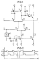
- FIG. 1 shows a circuit-like exemplary embodiment of a sample and hold circuit according to the invention
- 2 shows in a time diagram different pulse-pause ratios with regard to sample and hold pulses.
- the transistors T1, T2, T3 and T4 form a differential amplifier.
- the transistors are bipolar transistors.
- On A charging capacitor C1 is connected to the output.
- An output circuit also connected to its output is formed with the help of transistors T5 and T6. These transistors form an output amplifier with an output terminal A.
- a sampling circuit which consists not only of the transistors T1 to T4 of the differential amplifier but also of further transistors T7, T9, T10, T11.
- the capacitor C1 can be charged by means of sampling pulses supplied via a terminal S, in accordance with the input signal present at the input terminal E.
- a signal voltage stored in each case on the capacitor is output via the output connection A, with the aid of the output circuit consisting of the transistors T5, T6 and T8, which is provided between the charging capacitor C1 and the output connection A.
- transistors T5 and T6 form the output amplifier mentioned.
- Both the differential amplifier formed from the transistors T1 to T4 and the output amplifier consisting of the transistors T5 and T6 are connected to constant current sources. These are formed with the help of transistors T7 and T8. These transistors are also bipolar transistors. These transistors are effectively controlled on the occurrence of the scanning pulses which arrive via the terminal S in accordance with the frequency of their occurrence, in such a way that the level of the constant current flowing through them is proportional to the respective scanning pulse frequency.
- the bipolar transistors T7 and T8, which form the constant current sources mentioned are connected on the input side to the output of a frequency-current converter MF. The scanning pulses from terminal S are fed to its input.
- the frequency-current converter mentioned is implemented as a monostable multivibrator. The same is triggered by the sampling pulses (arriving via S). With the output of this monostable multivibrator is a further capacitor C2 via a resistor R. connected.
- the base connections of the bipolar transistors T7 and T8 of the constant current sources are connected to it.
- a further bipolar transistor T9 is connected, which arrives directly into the conductive one through the scanning pulses (arriving via S) Condition is controllable.
- the output of the output amplifier which is formed from the bipolar transistors T5 and T6, is also connected to the inverting input of the differential amplifier, which is formed from the bipolar transistors T1 to T4.
- the monostable flip-flop MF triggers a pulse of constant width for each scanning pulse (arriving via S). This is shown in FIG 2. (Incoming sampling pulses of different widths are shown in FIG. 2 at ts.)
- the pulse which is respectively passed on via the monostable flip-flop MF and which is passed on via the terminal v and the resistor R is in each case of a constant width.
- the constant current Io that flows across the collector of the bipolar transistor T7 is exactly proportional to the sampling pulse frequency.
- the desired goal has thus been achieved: the larger the constant current I0, the faster the capacitor C1 charges - and this in turn depends on the sampling rate; and the discharge of the capacitor C1 via the base current T5 / T6 is dependent on I0 and thus on the sampling rate.
- the pulse-pause ratio of the sampling pulses is always constant, which means that the mean value of the voltage in question is also constant.
Landscapes
- Amplifiers (AREA)
- Transforming Light Signals Into Electric Signals (AREA)
- Exchange Systems With Centralized Control (AREA)
Priority Applications (1)
| Application Number | Priority Date | Filing Date | Title |
|---|---|---|---|
| AT88117130T ATE103094T1 (de) | 1987-12-11 | 1988-10-14 | Abtast- und halteschaltung fuer fernmeldeanlagen. |
Applications Claiming Priority (2)
| Application Number | Priority Date | Filing Date | Title |
|---|---|---|---|
| DE3742115 | 1987-12-11 | ||
| DE3742115 | 1987-12-11 |
Publications (3)
| Publication Number | Publication Date |
|---|---|
| EP0319677A2 true EP0319677A2 (fr) | 1989-06-14 |
| EP0319677A3 EP0319677A3 (fr) | 1991-03-06 |
| EP0319677B1 EP0319677B1 (fr) | 1994-03-16 |
Family
ID=6342424
Family Applications (1)
| Application Number | Title | Priority Date | Filing Date |
|---|---|---|---|
| EP88117130A Expired - Lifetime EP0319677B1 (fr) | 1987-12-11 | 1988-10-14 | Circuit d'échantillonnage et de maintien pour systèmes de télécommunications |
Country Status (3)
| Country | Link |
|---|---|
| EP (1) | EP0319677B1 (fr) |
| AT (1) | ATE103094T1 (fr) |
| DE (1) | DE3888471D1 (fr) |
Family Cites Families (1)
| Publication number | Priority date | Publication date | Assignee | Title |
|---|---|---|---|---|
| AT280356B (de) * | 1968-03-06 | 1970-04-10 | Telefonbau & Normalzeit Gmbh | Schaltungsanordnung zur Steuerung des zur Zwischenspeicherung des Zeitwertes eines Signales verwendeten Kondensators eines Demodulators einer Zeitmultiplexanlage |
-
1988
- 1988-10-14 EP EP88117130A patent/EP0319677B1/fr not_active Expired - Lifetime
- 1988-10-14 AT AT88117130T patent/ATE103094T1/de active
- 1988-10-14 DE DE88117130T patent/DE3888471D1/de not_active Expired - Fee Related
Also Published As
| Publication number | Publication date |
|---|---|
| ATE103094T1 (de) | 1994-04-15 |
| EP0319677A3 (fr) | 1991-03-06 |
| EP0319677B1 (fr) | 1994-03-16 |
| DE3888471D1 (de) | 1994-04-21 |
Similar Documents
| Publication | Publication Date | Title |
|---|---|---|
| DE3342735C2 (fr) | ||
| DE2323478A1 (de) | Datenuebertragungsanordnung | |
| DE2059933C3 (de) | Digital-Analog-Umsetzer | |
| DE69320326T2 (de) | Mit niedriger Versorgungsspannung arbeitender, eine Hysteresis aufweisender Komparator | |
| DE3119923C2 (de) | Schaltungsanordnung für einen Bereichskomparator | |
| DE3743603C2 (fr) | ||
| DE3147547C2 (de) | Durch einen Übernahmetakt gesteuertes Flipflop in Stromumschaltetechnik | |
| EP0077500A2 (fr) | Diviseur de fréquence intégrable | |
| EP0319677B1 (fr) | Circuit d'échantillonnage et de maintien pour systèmes de télécommunications | |
| DE69005312T2 (de) | Stromart abtast-und-halteverstärker. | |
| DE3113824C2 (de) | Verstärker mit Mitteln zum Unterdrücken von Gleichspannungssprüngen am Verstärkerausgang | |
| DE2056078B2 (de) | Rueckgekoppelter verriegelungsschalter | |
| DE2503384C3 (de) | Differenzverstärker für den Subnanosekundenbereich | |
| DE2445799B2 (de) | Monostabiler Multivibrator | |
| DE1246027B (de) | Logische Schaltung aus zwei in Stromuebernahme-schaltung geschalteten Transistoren | |
| DE4101577A1 (de) | Transkonduktanzverstaerker | |
| DE19812972B4 (de) | Integratorschaltung | |
| DE2747281A1 (de) | Sprossendaempfer | |
| DE1254194B (de) | Negativer Impedanzwandler unter Verwendung eines gleichstromgekoppelten, spulenfreien Transistorverstaerkers | |
| DE2608431B2 (de) | Aus zwei allpassgliedern erster ordnung gebildete spulenlose filterschaltung | |
| DE1814887A1 (de) | Transistorverstaerkerschaltung | |
| DE2740954C2 (de) | Basisgekoppelte bistabile Logikschaltung | |
| DE2163628C3 (de) | Elektronische Verzögerungsschaltung | |
| DE1914071B2 (de) | Schaltungsanordnung zur automatischen pegelregelung | |
| DE2158881A1 (de) | Video-verstaerker mit gleichstromfreiem ausgang |
Legal Events
| Date | Code | Title | Description |
|---|---|---|---|
| PUAI | Public reference made under article 153(3) epc to a published international application that has entered the european phase |
Free format text: ORIGINAL CODE: 0009012 |
|
| AK | Designated contracting states |
Kind code of ref document: A2 Designated state(s): AT BE CH DE FR GB IT LI NL SE |
|
| PUAL | Search report despatched |
Free format text: ORIGINAL CODE: 0009013 |
|
| 17P | Request for examination filed |
Effective date: 19901205 |
|
| AK | Designated contracting states |
Kind code of ref document: A3 Designated state(s): AT BE CH DE FR GB IT LI NL SE |
|
| 17Q | First examination report despatched |
Effective date: 19930125 |
|
| GRAA | (expected) grant |
Free format text: ORIGINAL CODE: 0009210 |
|
| AK | Designated contracting states |
Kind code of ref document: B1 Designated state(s): AT BE CH DE FR GB IT LI NL SE |
|
| REF | Corresponds to: |
Ref document number: 103094 Country of ref document: AT Date of ref document: 19940415 Kind code of ref document: T |
|
| REF | Corresponds to: |
Ref document number: 3888471 Country of ref document: DE Date of ref document: 19940421 |
|
| ITF | It: translation for a ep patent filed | ||
| GBT | Gb: translation of ep patent filed (gb section 77(6)(a)/1977) |
Effective date: 19940525 |
|
| ET | Fr: translation filed | ||
| PLBE | No opposition filed within time limit |
Free format text: ORIGINAL CODE: 0009261 |
|
| STAA | Information on the status of an ep patent application or granted ep patent |
Free format text: STATUS: NO OPPOSITION FILED WITHIN TIME LIMIT |
|
| EAL | Se: european patent in force in sweden |
Ref document number: 88117130.0 |
|
| 26N | No opposition filed | ||
| PGFP | Annual fee paid to national office [announced via postgrant information from national office to epo] |
Ref country code: GB Payment date: 19980909 Year of fee payment: 11 |
|
| PGFP | Annual fee paid to national office [announced via postgrant information from national office to epo] |
Ref country code: AT Payment date: 19980929 Year of fee payment: 11 |
|
| PGFP | Annual fee paid to national office [announced via postgrant information from national office to epo] |
Ref country code: BE Payment date: 19981016 Year of fee payment: 11 |
|
| PGFP | Annual fee paid to national office [announced via postgrant information from national office to epo] |
Ref country code: FR Payment date: 19981023 Year of fee payment: 11 |
|
| PGFP | Annual fee paid to national office [announced via postgrant information from national office to epo] |
Ref country code: SE Payment date: 19981027 Year of fee payment: 11 |
|
| PGFP | Annual fee paid to national office [announced via postgrant information from national office to epo] |
Ref country code: NL Payment date: 19981030 Year of fee payment: 11 |
|
| PGFP | Annual fee paid to national office [announced via postgrant information from national office to epo] |
Ref country code: DE Payment date: 19981217 Year of fee payment: 11 |
|
| PGFP | Annual fee paid to national office [announced via postgrant information from national office to epo] |
Ref country code: CH Payment date: 19990119 Year of fee payment: 11 |
|
| PG25 | Lapsed in a contracting state [announced via postgrant information from national office to epo] |
Ref country code: GB Free format text: LAPSE BECAUSE OF NON-PAYMENT OF DUE FEES Effective date: 19991014 Ref country code: AT Free format text: LAPSE BECAUSE OF NON-PAYMENT OF DUE FEES Effective date: 19991014 |
|
| PG25 | Lapsed in a contracting state [announced via postgrant information from national office to epo] |
Ref country code: SE Free format text: THE PATENT HAS BEEN ANNULLED BY A DECISION OF A NATIONAL AUTHORITY Effective date: 19991030 |
|
| PG25 | Lapsed in a contracting state [announced via postgrant information from national office to epo] |
Ref country code: LI Free format text: LAPSE BECAUSE OF NON-PAYMENT OF DUE FEES Effective date: 19991031 Ref country code: CH Free format text: LAPSE BECAUSE OF NON-PAYMENT OF DUE FEES Effective date: 19991031 Ref country code: BE Free format text: LAPSE BECAUSE OF NON-PAYMENT OF DUE FEES Effective date: 19991031 |
|
| BERE | Be: lapsed |
Owner name: SIEMENS A.G. Effective date: 19991031 |
|
| PG25 | Lapsed in a contracting state [announced via postgrant information from national office to epo] |
Ref country code: NL Free format text: LAPSE BECAUSE OF NON-PAYMENT OF DUE FEES Effective date: 20000501 |
|
| GBPC | Gb: european patent ceased through non-payment of renewal fee |
Effective date: 19991014 |
|
| REG | Reference to a national code |
Ref country code: CH Ref legal event code: PL |
|
| EUG | Se: european patent has lapsed |
Ref document number: 88117130.0 |
|
| PG25 | Lapsed in a contracting state [announced via postgrant information from national office to epo] |
Ref country code: FR Free format text: LAPSE BECAUSE OF NON-PAYMENT OF DUE FEES Effective date: 20000630 |
|
| NLV4 | Nl: lapsed or anulled due to non-payment of the annual fee |
Effective date: 20000501 |
|
| PG25 | Lapsed in a contracting state [announced via postgrant information from national office to epo] |
Ref country code: DE Free format text: LAPSE BECAUSE OF NON-PAYMENT OF DUE FEES Effective date: 20000801 |
|
| REG | Reference to a national code |
Ref country code: FR Ref legal event code: ST |
|
| PG25 | Lapsed in a contracting state [announced via postgrant information from national office to epo] |
Ref country code: IT Free format text: LAPSE BECAUSE OF NON-PAYMENT OF DUE FEES;WARNING: LAPSES OF ITALIAN PATENTS WITH EFFECTIVE DATE BEFORE 2007 MAY HAVE OCCURRED AT ANY TIME BEFORE 2007. THE CORRECT EFFECTIVE DATE MAY BE DIFFERENT FROM THE ONE RECORDED. Effective date: 20051014 |