EP0319799A2 - Circuit et procédé d'amélioration de la robustesse de registre - Google Patents
Circuit et procédé d'amélioration de la robustesse de registre Download PDFInfo
- Publication number
- EP0319799A2 EP0319799A2 EP88119698A EP88119698A EP0319799A2 EP 0319799 A2 EP0319799 A2 EP 0319799A2 EP 88119698 A EP88119698 A EP 88119698A EP 88119698 A EP88119698 A EP 88119698A EP 0319799 A2 EP0319799 A2 EP 0319799A2
- Authority
- EP
- European Patent Office
- Prior art keywords
- data
- register
- input data
- accordance
- registers
- Prior art date
- Legal status (The legal status is an assumption and is not a legal conclusion. Google has not performed a legal analysis and makes no representation as to the accuracy of the status listed.)
- Withdrawn
Links
Images


Classifications
-
- G—PHYSICS
- G06—COMPUTING OR CALCULATING; COUNTING
- G06F—ELECTRIC DIGITAL DATA PROCESSING
- G06F11/00—Error detection; Error correction; Monitoring
- G06F11/07—Responding to the occurrence of a fault, e.g. fault tolerance
- G06F11/16—Error detection or correction of the data by redundancy in hardware
- G06F11/1666—Error detection or correction of the data by redundancy in hardware where the redundant component is memory or memory area
- G06F11/167—Error detection by comparing the memory output
-
- G—PHYSICS
- G06—COMPUTING OR CALCULATING; COUNTING
- G06F—ELECTRIC DIGITAL DATA PROCESSING
- G06F11/00—Error detection; Error correction; Monitoring
- G06F11/07—Responding to the occurrence of a fault, e.g. fault tolerance
- G06F11/14—Error detection or correction of the data by redundancy in operations
-
- G—PHYSICS
- G06—COMPUTING OR CALCULATING; COUNTING
- G06F—ELECTRIC DIGITAL DATA PROCESSING
- G06F11/00—Error detection; Error correction; Monitoring
- G06F11/07—Responding to the occurrence of a fault, e.g. fault tolerance
- G06F11/16—Error detection or correction of the data by redundancy in hardware
- G06F11/1608—Error detection by comparing the output signals of redundant hardware
- G06F11/1625—Error detection by comparing the output signals of redundant hardware in communications, e.g. transmission, interfaces
-
- G—PHYSICS
- G06—COMPUTING OR CALCULATING; COUNTING
- G06F—ELECTRIC DIGITAL DATA PROCESSING
- G06F11/00—Error detection; Error correction; Monitoring
-
- G—PHYSICS
- G06—COMPUTING OR CALCULATING; COUNTING
- G06F—ELECTRIC DIGITAL DATA PROCESSING
- G06F11/00—Error detection; Error correction; Monitoring
- G06F11/07—Responding to the occurrence of a fault, e.g. fault tolerance
- G06F11/0796—Safety measures, i.e. ensuring safe condition in the event of error, e.g. for controlling element
Definitions
- the present invention relates generally to the field of data transmission, and specifically to circuitry for protecting hardware and critical data control circuits from the consequences of a data control failure, resulting from software or firmware failures.
- the present invention also relates to a data register robustness circuit.
- critical circuit control points provide data traffic path switching and control, all under the direction of software instructions, which may be stored in integrated circuit ROM and EPROM or other memories.
- software instructions which may be stored in integrated circuit ROM and EPROM or other memories.
- the potential for losing telecommunication traffic is great, hence it is a current practice in the telecommunications industry to duplicate much of the critical hardware, and to substitute spare circuitry for failed circuitry in the event of a hardware fault, thereby maintaining the traffic.
- Certain of the hardware control functions are directed by and are under the control of software as mentioned before, and errors in this software can cause the hardware to malfunction, since such hardware contains control points that are accessed by the software by simple read and write instructions. When the software fails so as to accidentally write to one or more control points, or to couple erroneous data to such control points, traffic can be lost.
- the present invention provides a circuit which is interposed between the control points and the control software to detect the aforementioned erroneous control transmissions and to ensure that only accurate control data is coupled to the control points.
- a circuit is described which requires the control software to write the same data to a control point register twice in immediate sequence before the intended action can occur. Since the typical failure mode of control software is to start reading and writing random data to random locations, the present invention provides substantially improved robustness and protection against almost all normal software failures, since under such failure conditions, the same data would not be written to the same location two times in immediate sequence.
- the known prior art includes various redundant signal processors which require duplication of hardware or complex and costly circuit arrangements, in contradistinction to the present invention.
- Examples of such prior art techniques are U.S. Patent 3,883,891, titled redundant signal processing error reduction technique; U.S. Patent 4,344,180 titled redundant word frame sunchronization circuit; U.S. Patent 4,453,215 titled central processing apparatus for fault-tolerant computing; U.S. Patent 3,800,286 titled address development techniques utilizing a content addressable memory; U.S. Patent 4,130,241 titled control systems; and U.S. Patent 4,456,997 titled facility for fail-safe data transmission between trackside equipment.
- None of the aforementioned prior art patents provide for the simplified technique of duplication of data and bit-by-bit comparison of the duplicated data in a robust register circuit, which overcomes the complexity and cost of the prior art, while Protecting critical control points against software failures, as provided by the present invention.
- a further object of the invention is to provide a robust register circuit and method which requires that control data must be written twice in a row before it is recognized as valid data and coupled to a critical control point.
- the present invention describes a robust register circuit for protecting critical control points in data transmission and telecommunications equipment against software induced failures.
- a circuit is provided wherein duplicated data words are written into a pair of registers of any desired bit length.
- a digital comparator determines whether the two data words are the same, and initiates a data transfer into a third register for transmission to critical hardware control points only when two identical sequential data words are recognized. When no such recognition occurs, new data is not transferred to the third register, and the hardware control points remain controlled by the previous data in the third register.
- FIG. 1 a block diagram of a circuit for protecting circuit control points, such as telecommunications traffic control points, protection switch relay control inputs, and any relatively static control points from erroneous data inputs is illustrated generally at 10.
- the data input to protection circuit 10 is shown at line 12, which is representative of any number of data bits from a processor under software control.
- processors are well known off-the-shelf microprocessors, for example, which contain programming stored in ROM.
- Such stored programming is in the form of instructions or addresses in memory, and may initiate multi-bit instruction or address data words onto line 12.
- 7-bit data words are operated upon, by way of example, however, any length data words may be accomodated.
- ROM read-only-memory
- EPROM electrically programmable read-only-memory
- Such a change of state of a stored data bit can result in an erroneous instruction being read onto line 12 from ROM or EPROM, such as "go to RAM” instead of ROM, causing control software to try to execute data instead of code.
- the circuit 10 is located between the processor output on line 12 and the control point input 14, thereby, as will be explained hereinafter, preventing erroneous data from being coupled to critical control points.
- the circuit 10 functions to require that any data on line 12 must be transmitted in duplicate, such that identical data bit sequences must be recognized twice in a row, i.e. two identical 7-bit binary number sequences immediately following each other in direct sequence, with no other data bits in between. Only when the foregoing condition is met is data coupled out on line 14 to the critical control points.
- control point Since these control points are not changed very often, eg. are relatively static, high data speed is not critical to the intended protective circuit operation.
- a control point is, for example, a protection switch relay to switch telecommunications traffic from line one line card to another when a fault occurs in the line card.
- the doubling of the time for real time processing is no disadvantage in such applications.
- Sequencer and steering logic circuit 16 receives READ and WRITE commands on line 18 from a processor (which does not form a part of the invention, and can consist of any known source of such instructions).
- the sequencer 16 must recognize the proper sequence of READS and WRITES to properly operate. Specifically, the instruction on line 18 must first READ, then WRITE, then WRITE again the same data on line 12 to the same register address on line 20.
- the READ input on line 18 resets the sequencer 16 so that it points to register 1, shown at 22.
- the WRITE instruction generates a waveform to clock the first data word from line 12 to register 1, and advances the sequencer 16 so that it points to register 2, shown at 24; the next WRITE instruction on line 18 clocks the second data word from line 12 into register 2.
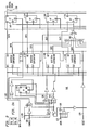
- FIG. 1 a schematic diagram of the circuit of Figure 1 is shown generally at 100. While this circuit can be implemented either in discrete or integrated circuit logic, the circuit shown is implemented in a gate array in CMOS in an LSI Logic 9000 series using a 1.2 micron process.
- Each of the register/comparator circuits 104, 106, 108, 110, 112, 114 and 116 includes a single bit circuit incorporating registers 1 and 2 and comparator 26 of Figure 1.
- the seven register/comparator circuits 104-116 taken together implement registers 1, 2 and comparator 26 of Figure 1.
- the seven register/comparator circuits 104-116 taken together implement registers 1, 2 and comparator 26 of Figure 1 in their entirety.
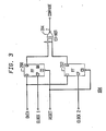
- Figure 3 illustrates the circuit details for handling a single bit of registers 1, 2 and comparator 26, and corresponds to any one of the circuits 104 through 116, in detail.
- An asynchronous reset signal RESET on line 118 is applied during initialization, and clears all registers and resets the pointer flip-flop 120 in the sequencer and steering logic circuit 16.
- the register address on line 122 is decoded by a four input NAND gate 124 to derive an active-low signal on line 126, which is applied whenever the register is being addressed by control software on line 20. Any read cycle to the addressed register is decoded from logic high from line 128, active low from line 126, and active low from line 130 by NAND gate 132, which resets the pointer flip-flop 120.
- a write cycle to the register is decoded from low on line 128, low on line 126 and active-low pulse on line 130 and appears at the input to NAND gates 134 and 136.
- the sequencer 16 operation will now be described.
- the proper input sequence is READ, WRITE, WRITE.
- the first READ operation assures that the pointer flip-flop 120 is reset. This enables NAND gate 134, which allows the enable pulse on line 130 during the first WRITE cycle to clock the data from the DATA IN bus 102 into the first register 104 of the register/comparators 104-116.
- the foregoing operation also sets flip-flop 138.
- the pointer flip-flop 120 is set, which enables NAND gate 136, which allows the enable pulse during the next WRITE cycle to clock the data from line 102 into the register 2 (described with reference to Figure 1) of each of the register/comparator circuits 104 through 116 of Figure 2.
- Each bit of the two registers 1 and 2 contained in each of circuits 104 through 116 is compared with the other bit by the individual comparator 26 in each circuit 104 through 116, which comparator 26 is implemented for each bit to be compared by the exclusive-NOR gate 204 described with reference to Figure 3.
- Figure 3 illustrates a register/comparator circuit 104, which comprises flip-flops 200 and 202 and exclusive-NOR gate 204.
- Exclusive-NOR gate 204 is one seventh of the digital comparator 26
- flip-flop 200 corresponds to one seventh of register 2
- flip-flop 202 corresponds to one seventh of register 1.
- Circuits 106 through 116 are identical to circuit 104.
- the comparisons from each of the comparators in circuits 104 through 116 are logically ANDed by NAND gate 140.
- NAND gate 140 is enabled by flip-flop 138, which monitors the decoded register address from NAND gate 124 for activity. Any change on the address bus during the WRITE operations clears flip-flop 138, which in turn disables the comparators NAND gate 140, thereby preventing completion of the cycle.
- register 1 and 2 contents at comparator 26 is indicative of valid data, e.g. no change of address
- the rising edge of the enable pulse clocks register 2 data into register 3 (shown as 32 in Figure 1), and comprising flip-flops 142, 144, 146, 148, 150, 152 and 154 as shown in Figure 2.
- the output of register 3, eg. the 7-bit output of registers 142 through 154, is coupled out to the critical hardware control points via line 156, which corresponds to line 14 in Figure 1.
Landscapes
- Engineering & Computer Science (AREA)
- Theoretical Computer Science (AREA)
- Quality & Reliability (AREA)
- Physics & Mathematics (AREA)
- General Engineering & Computer Science (AREA)
- General Physics & Mathematics (AREA)
- Logic Circuits (AREA)
- Hardware Redundancy (AREA)
- Detection And Prevention Of Errors In Transmission (AREA)
Applications Claiming Priority (2)
| Application Number | Priority Date | Filing Date | Title |
|---|---|---|---|
| US07/130,850 US4959836A (en) | 1987-12-09 | 1987-12-09 | Register robustness improvement circuit and method |
| US130850 | 1987-12-09 |
Publications (2)
| Publication Number | Publication Date |
|---|---|
| EP0319799A2 true EP0319799A2 (fr) | 1989-06-14 |
| EP0319799A3 EP0319799A3 (fr) | 1991-02-06 |
Family
ID=22446656
Family Applications (1)
| Application Number | Title | Priority Date | Filing Date |
|---|---|---|---|
| EP19880119698 Withdrawn EP0319799A3 (fr) | 1987-12-09 | 1988-11-25 | Circuit et procédé d'amélioration de la robustesse de registre |
Country Status (3)
| Country | Link |
|---|---|
| US (1) | US4959836A (fr) |
| EP (1) | EP0319799A3 (fr) |
| NO (1) | NO885485L (fr) |
Cited By (3)
| Publication number | Priority date | Publication date | Assignee | Title |
|---|---|---|---|---|
| FR2705803A1 (fr) * | 1993-05-26 | 1994-12-02 | Gemplus Card Int | Procédé d'écriture d'informations dans une mémoire non-volatile. |
| EP1962193A1 (fr) | 2007-02-19 | 2008-08-27 | Continental Automotive GmbH | Dispositif de circuit pour la commande d'une charge et procédé correspondant |
| WO2019069042A1 (fr) * | 2017-10-05 | 2019-04-11 | Arm Limited | Gestion d'erreurs dans des tampons |
Families Citing this family (12)
| Publication number | Priority date | Publication date | Assignee | Title |
|---|---|---|---|---|
| JPH0344898A (ja) * | 1989-07-12 | 1991-02-26 | Ando Electric Co Ltd | チェックサム値を照合するpromライタ |
| EP0453863A2 (fr) * | 1990-04-27 | 1991-10-30 | National Semiconductor Corporation | Méthode et appareil pour réaliser le contrôle d'accès au média/interface avec le système hôte |
| JP2803351B2 (ja) * | 1990-09-14 | 1998-09-24 | 日本電気株式会社 | 多数決回路 |
| DE4326919A1 (de) * | 1993-08-11 | 1995-02-16 | Teves Gmbh Alfred | Regelschaltung für Bremsanlagen mit ABS und/oder ASR |
| JPH1041927A (ja) * | 1996-05-24 | 1998-02-13 | Kansei Corp | 多重通信方法及びその装置 |
| US7318169B2 (en) * | 2002-05-15 | 2008-01-08 | David Czajkowski | Fault tolerant computer |
| US7237148B2 (en) * | 2002-09-05 | 2007-06-26 | David Czajkowski | Functional interrupt mitigation for fault tolerant computer |
| US7260742B2 (en) * | 2003-01-28 | 2007-08-21 | Czajkowski David R | SEU and SEFI fault tolerant computer |
| DE102004021088A1 (de) * | 2004-04-29 | 2005-11-17 | Giesecke & Devrient Gmbh | Verfahren zum Schützen von Daten eines Datenträgers gegen DFA-Angriffe |
| US7392426B2 (en) * | 2004-06-15 | 2008-06-24 | Honeywell International Inc. | Redundant processing architecture for single fault tolerance |
| US7251759B2 (en) * | 2004-08-16 | 2007-07-31 | Broadcom Corporation | Method and apparatus to compare pointers associated with asynchronous clock domains |
| US20060236168A1 (en) * | 2005-04-01 | 2006-10-19 | Honeywell International Inc. | System and method for dynamically optimizing performance and reliability of redundant processing systems |
Family Cites Families (37)
| Publication number | Priority date | Publication date | Assignee | Title |
|---|---|---|---|---|
| DE98576C (fr) * | ||||
| DE159681C (fr) * | ||||
| US3430204A (en) * | 1965-05-19 | 1969-02-25 | Gen Electric | Data communication system employing an asynchronous start-stop clock generator |
| US3562708A (en) * | 1968-06-24 | 1971-02-09 | Mc Donnell Douglas Corp | Device to eliminate undersirable transient effects on computer operations and the like |
| US3624603A (en) * | 1969-09-16 | 1971-11-30 | Gen Electric | Digital data communications system with means for improving system security |
| DE1965314C3 (de) * | 1969-12-29 | 1974-10-17 | Siemens Ag, 1000 Berlin Und 8000 Muenchen | Verfahren zum Betrieb einer Datenverarbeitungsanordnung mit zwei Datenverarbeitungsanlagen |
| US3732541A (en) * | 1970-04-27 | 1973-05-08 | Licentia Gmbh | Method and apparatus for evaluating repetitively transmitted signals |
| US3781792A (en) * | 1972-01-03 | 1973-12-25 | British Railways Board | Error detection in communication system by repetition of data |
| US3800286A (en) * | 1972-08-24 | 1974-03-26 | Honeywell Inf Systems | Address development technique utilizing a content addressable memory |
| US3863215A (en) * | 1973-07-03 | 1975-01-28 | Rca Corp | Detector for repetitive digital codes |
| DE2347317A1 (de) * | 1973-09-20 | 1975-04-03 | Licentia Gmbh | Schaltungsanordnung zur erzeugung von pruefstellen in anlagen zur gesicherten datenuebertragung |
| US3876980A (en) * | 1973-11-05 | 1975-04-08 | Products Of Information Techno | Vehicle location systems |
| US4042923A (en) * | 1973-11-30 | 1977-08-16 | Del Norte Technology, Inc. | Radar trilateralization position locators |
| US3883891A (en) * | 1974-08-22 | 1975-05-13 | Rca Corp | Redundant signal processing error reduction technique |
| SU647694A1 (ru) * | 1976-01-22 | 1979-02-15 | Podunaev Georgij A | Устройство дл проверки монтажных схем |
| DE2609107A1 (de) * | 1976-03-05 | 1977-09-08 | Standard Elektrik Lorenz Ag | Schaltung zur sicherung uebermittelter daten |
| FR2344063A1 (fr) * | 1976-03-10 | 1977-10-07 | Smiths Industries Ltd | Circuit numerique de commande a deux voies au moins |
| SU593214A1 (ru) * | 1976-05-21 | 1978-02-15 | Предприятие П/Я А-3706 | Вычислительное устройство |
| DE2640756C2 (de) * | 1976-09-10 | 1982-11-04 | Standard Elektrik Lorenz Ag, 7000 Stuttgart | Einrichtung zur gesicherten Datenübertragung bei spurgebundenen Fahrzeugen |
| US4245212A (en) * | 1978-03-13 | 1981-01-13 | The United States Of America As Represented By The Secretary Of The Navy | Serial digital data decoder |
| SU676984A1 (ru) * | 1978-03-20 | 1979-07-30 | Войсковая Часть 11284 | Устройство дл ввода информации |
| US4233682A (en) * | 1978-06-15 | 1980-11-11 | Sperry Corporation | Fault detection and isolation system |
| GB2032736B (en) * | 1978-10-24 | 1982-09-08 | Standard Telephones Cables Ltd | Data transfer system |
| DE2936439C2 (de) * | 1979-09-08 | 1983-02-17 | Wabco Westinghouse Fahrzeugbremsen GmbH, 3000 Hannover | Anordnung zur asynchronen Übertragung von digitalen Radgeschwindigkeits-Meßwerten |
| DE3012159C2 (de) * | 1980-03-26 | 1982-09-02 | Licentia Patent-Verwaltungs-Gmbh, 6000 Frankfurt | Anordnung zur gesicherten Datenausgabe |
| US4344180A (en) * | 1980-06-19 | 1982-08-10 | Bell Telephone Laboratories, Incorporated | Redundant word frame synchronization circuit |
| DE3040080C1 (de) * | 1980-10-24 | 1987-11-12 | Standard Elektrik Lorenz Ag, 7000 Stuttgart | Einrichtung zur signaltechnisch sicheren Datenuebertragung zwischen einer Trasse und auf dieser gefuehrten Fahrzeugen |
| JPS57152037A (en) * | 1981-03-16 | 1982-09-20 | Toshiba Corp | Checking method for operation of data transmitter |
| US4486826A (en) * | 1981-10-01 | 1984-12-04 | Stratus Computer, Inc. | Computer peripheral control apparatus |
| CH663304A5 (de) * | 1982-06-16 | 1987-11-30 | Siemens Ag Albis | Anordnung zur gesicherten uebertragung von daten ueber busleitungen. |
| JPS5960786A (ja) * | 1982-09-30 | 1984-04-06 | Fujitsu Ltd | 半導体集積回路 |
| US4599708A (en) * | 1983-12-30 | 1986-07-08 | International Business Machines Corporation | Method and structure for machine data storage with simultaneous write and read |
| DE3412049A1 (de) * | 1984-03-30 | 1985-10-17 | Licentia Patent-Verwaltungs-Gmbh, 6000 Frankfurt | Signaltechnisch sichere datenverarbeitungseinrichtung |
| GB8415996D0 (en) * | 1984-06-22 | 1984-07-25 | Bank Of England | Image model |
| DE3431304A1 (de) * | 1984-08-25 | 1986-03-06 | Philips Patentverwaltung Gmbh, 2000 Hamburg | Verfahren und schaltungsanordnung zur triggerung eines logikanalysators |
| JPH0648822B2 (ja) * | 1985-03-04 | 1994-06-22 | 株式会社日立製作所 | デイジタル伝送系における異常処理方法 |
| US4751639A (en) * | 1985-06-24 | 1988-06-14 | Ncr Corporation | Virtual command rollback in a fault tolerant data processing system |
-
1987
- 1987-12-09 US US07/130,850 patent/US4959836A/en not_active Expired - Lifetime
-
1988
- 1988-11-25 EP EP19880119698 patent/EP0319799A3/fr not_active Withdrawn
- 1988-12-09 NO NO88885485A patent/NO885485L/no unknown
Cited By (6)
| Publication number | Priority date | Publication date | Assignee | Title |
|---|---|---|---|---|
| FR2705803A1 (fr) * | 1993-05-26 | 1994-12-02 | Gemplus Card Int | Procédé d'écriture d'informations dans une mémoire non-volatile. |
| WO1994028521A1 (fr) * | 1993-05-26 | 1994-12-08 | Gemplus Card International | Procede d'ecriture d'informations dans une memoire non-volatile |
| US5850506A (en) * | 1993-05-26 | 1998-12-15 | Gemplus Card International | Method of writing information in a non-volatile memory |
| EP1962193A1 (fr) | 2007-02-19 | 2008-08-27 | Continental Automotive GmbH | Dispositif de circuit pour la commande d'une charge et procédé correspondant |
| WO2019069042A1 (fr) * | 2017-10-05 | 2019-04-11 | Arm Limited | Gestion d'erreurs dans des tampons |
| US11113164B2 (en) | 2017-10-05 | 2021-09-07 | Arm Limited | Handling errors in buffers |
Also Published As
| Publication number | Publication date |
|---|---|
| NO885485D0 (no) | 1988-12-09 |
| NO885485L (no) | 1989-06-12 |
| EP0319799A3 (fr) | 1991-02-06 |
| US4959836A (en) | 1990-09-25 |
Similar Documents
| Publication | Publication Date | Title |
|---|---|---|
| US4959836A (en) | Register robustness improvement circuit and method | |
| US5408645A (en) | Circuit and method for detecting a failure in a microcomputer | |
| EP0363863B1 (fr) | Procédé et dispositif de recouvrement après erreur dans un système de calcul numérique | |
| US4541094A (en) | Self-checking computer circuitry | |
| US4296494A (en) | Error correction and detection systems | |
| US5068851A (en) | Apparatus and method for documenting faults in computing modules | |
| US4670880A (en) | Method of error detection and correction by majority | |
| EP0273043B1 (fr) | Systeme de detection d'erreurs a redondance triple et procede d'utilisation relatif | |
| US4852100A (en) | Error detection and correction scheme for main storage unit | |
| US4295219A (en) | Memory write error detection circuit | |
| US3568153A (en) | Memory with error correction | |
| US5048022A (en) | Memory device with transfer of ECC signals on time division multiplexed bidirectional lines | |
| US4942575A (en) | Error connection device for parity protected memory systems | |
| US3809884A (en) | Apparatus and method for a variable memory cycle in a data processing unit | |
| US4596014A (en) | I/O rack addressing error detection for process control | |
| US3898443A (en) | Memory fault correction system | |
| EP0279396B1 (fr) | Antémémoire comportant l'autovérification d'erreur et des circuits de vérification séquentiels | |
| EP0383899B1 (fr) | Detection d'erreur pour operation d'ecriture partielle pour des memoires | |
| US7346812B1 (en) | Apparatus and method for implementing programmable levels of error severity | |
| US4761783A (en) | Apparatus and method for reporting occurrences of errors in signals stored in a data processor | |
| EP0130429B1 (fr) | Appareil de détection d'erreur | |
| US4225959A (en) | Tri-state bussing system | |
| EP0142983B1 (fr) | Flip-flop de protection de faute | |
| US4254464A (en) | Common data buffer system | |
| IE892223A1 (en) | Improvements in and relating to stable memory circuits |
Legal Events
| Date | Code | Title | Description |
|---|---|---|---|
| PUAI | Public reference made under article 153(3) epc to a published international application that has entered the european phase |
Free format text: ORIGINAL CODE: 0009012 |
|
| AK | Designated contracting states |
Kind code of ref document: A2 Designated state(s): AT BE CH DE ES FR GB GR IT LI NL SE |
|
| PUAL | Search report despatched |
Free format text: ORIGINAL CODE: 0009013 |
|
| 17P | Request for examination filed |
Effective date: 19901205 |
|
| AK | Designated contracting states |
Kind code of ref document: A3 Designated state(s): AT BE CH DE ES FR GB GR IT LI NL SE |
|
| STAA | Information on the status of an ep patent application or granted ep patent |
Free format text: STATUS: THE APPLICATION IS DEEMED TO BE WITHDRAWN |
|
| 18D | Application deemed to be withdrawn |
Effective date: 19930602 |