EP0320016A1 - Dispositif de pulvérisation - Google Patents
Dispositif de pulvérisation Download PDFInfo
- Publication number
- EP0320016A1 EP0320016A1 EP88120657A EP88120657A EP0320016A1 EP 0320016 A1 EP0320016 A1 EP 0320016A1 EP 88120657 A EP88120657 A EP 88120657A EP 88120657 A EP88120657 A EP 88120657A EP 0320016 A1 EP0320016 A1 EP 0320016A1
- Authority
- EP
- European Patent Office
- Prior art keywords
- target
- sputtering
- temperature
- sputtering device
- heating
- Prior art date
- Legal status (The legal status is an assumption and is not a legal conclusion. Google has not performed a legal analysis and makes no representation as to the accuracy of the status listed.)
- Granted
Links
Images


Classifications
-
- C—CHEMISTRY; METALLURGY
- C23—COATING METALLIC MATERIAL; COATING MATERIAL WITH METALLIC MATERIAL; CHEMICAL SURFACE TREATMENT; DIFFUSION TREATMENT OF METALLIC MATERIAL; COATING BY VACUUM EVAPORATION, BY SPUTTERING, BY ION IMPLANTATION OR BY CHEMICAL VAPOUR DEPOSITION, IN GENERAL; INHIBITING CORROSION OF METALLIC MATERIAL OR INCRUSTATION IN GENERAL
- C23C—COATING METALLIC MATERIAL; COATING MATERIAL WITH METALLIC MATERIAL; SURFACE TREATMENT OF METALLIC MATERIAL BY DIFFUSION INTO THE SURFACE, BY CHEMICAL CONVERSION OR SUBSTITUTION; COATING BY VACUUM EVAPORATION, BY SPUTTERING, BY ION IMPLANTATION OR BY CHEMICAL VAPOUR DEPOSITION, IN GENERAL
- C23C14/00—Coating by vacuum evaporation, by sputtering or by ion implantation of the coating forming material
- C23C14/22—Coating by vacuum evaporation, by sputtering or by ion implantation of the coating forming material characterised by the process of coating
- C23C14/54—Controlling or regulating the coating process
- C23C14/541—Heating or cooling of the substrates
-
- H—ELECTRICITY
- H01—ELECTRIC ELEMENTS
- H01J—ELECTRIC DISCHARGE TUBES OR DISCHARGE LAMPS
- H01J37/00—Discharge tubes with provision for introducing objects or material to be exposed to the discharge, e.g. for the purpose of examination or processing thereof
- H01J37/32—Gas-filled discharge tubes
- H01J37/34—Gas-filled discharge tubes operating with cathodic sputtering
- H01J37/3411—Constructional aspects of the reactor
- H01J37/3447—Collimators, shutters, apertures
-
- C—CHEMISTRY; METALLURGY
- C23—COATING METALLIC MATERIAL; COATING MATERIAL WITH METALLIC MATERIAL; CHEMICAL SURFACE TREATMENT; DIFFUSION TREATMENT OF METALLIC MATERIAL; COATING BY VACUUM EVAPORATION, BY SPUTTERING, BY ION IMPLANTATION OR BY CHEMICAL VAPOUR DEPOSITION, IN GENERAL; INHIBITING CORROSION OF METALLIC MATERIAL OR INCRUSTATION IN GENERAL
- C23C—COATING METALLIC MATERIAL; COATING MATERIAL WITH METALLIC MATERIAL; SURFACE TREATMENT OF METALLIC MATERIAL BY DIFFUSION INTO THE SURFACE, BY CHEMICAL CONVERSION OR SUBSTITUTION; COATING BY VACUUM EVAPORATION, BY SPUTTERING, BY ION IMPLANTATION OR BY CHEMICAL VAPOUR DEPOSITION, IN GENERAL
- C23C14/00—Coating by vacuum evaporation, by sputtering or by ion implantation of the coating forming material
- C23C14/22—Coating by vacuum evaporation, by sputtering or by ion implantation of the coating forming material characterised by the process of coating
- C23C14/54—Controlling or regulating the coating process
-
- C—CHEMISTRY; METALLURGY
- C23—COATING METALLIC MATERIAL; COATING MATERIAL WITH METALLIC MATERIAL; CHEMICAL SURFACE TREATMENT; DIFFUSION TREATMENT OF METALLIC MATERIAL; COATING BY VACUUM EVAPORATION, BY SPUTTERING, BY ION IMPLANTATION OR BY CHEMICAL VAPOUR DEPOSITION, IN GENERAL; INHIBITING CORROSION OF METALLIC MATERIAL OR INCRUSTATION IN GENERAL
- C23C—COATING METALLIC MATERIAL; COATING MATERIAL WITH METALLIC MATERIAL; SURFACE TREATMENT OF METALLIC MATERIAL BY DIFFUSION INTO THE SURFACE, BY CHEMICAL CONVERSION OR SUBSTITUTION; COATING BY VACUUM EVAPORATION, BY SPUTTERING, BY ION IMPLANTATION OR BY CHEMICAL VAPOUR DEPOSITION, IN GENERAL
- C23C14/00—Coating by vacuum evaporation, by sputtering or by ion implantation of the coating forming material
- C23C14/22—Coating by vacuum evaporation, by sputtering or by ion implantation of the coating forming material characterised by the process of coating
- C23C14/56—Apparatus specially adapted for continuous coating; Arrangements for maintaining the vacuum, e.g. vacuum locks
- C23C14/564—Means for minimising impurities in the coating chamber such as dust, moisture, residual gases
-
- H—ELECTRICITY
- H01—ELECTRIC ELEMENTS
- H01J—ELECTRIC DISCHARGE TUBES OR DISCHARGE LAMPS
- H01J37/00—Discharge tubes with provision for introducing objects or material to be exposed to the discharge, e.g. for the purpose of examination or processing thereof
- H01J37/32—Gas-filled discharge tubes
- H01J37/34—Gas-filled discharge tubes operating with cathodic sputtering
-
- H—ELECTRICITY
- H01—ELECTRIC ELEMENTS
- H01J—ELECTRIC DISCHARGE TUBES OR DISCHARGE LAMPS
- H01J2237/00—Discharge tubes exposing object to beam, e.g. for analysis treatment, etching, imaging
- H01J2237/02—Details
- H01J2237/022—Avoiding or removing foreign or contaminating particles, debris or deposits on sample or tube
Definitions
- This invention relates to a device for manufacturing semiconductor devices, and more particularly to a sputtering device for depositing insulation or metal material on a semiconductor wafer substrate.
- a high speed sputtering device for effecting sputtering process for each semiconductor wafer substrate.
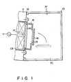
- Fig. 1 shows the internal structure of this type of high speed sputtering device.
- the sputtering process is repeatedly effected in vacuum chamber VC which is kept in a low pressure condition.
- the pressure in vacuum chamber VC is reduced with cathode case CS inserted in cathode flange 11 and cathode flange 11 set in contact with chamber wall 13 via O-ring 12.
- Target 16 is previously mounted on backing plate 17 in vacuum chamber VC with an angle of approx. 85° which is close to right angles with respect to a horizontal plane.
- semiconductor wafer substrate 19 is horizontally carried in pressure-reduced vaccum chamber VC, and is set onto substrate holder 18 disposed in a position corresponding to target 16. Substrate holder 18 is raised as shown by an arrow so as to set semiconductor wafer substrate 19 in parallel with target 16.
- the sputtering process is effected after semiconductor wafer substrate 19 is set in the above-described preset sputtering position.
- a sputtering film is formed by striking Ar+ ions to target 16 in the magnetron discharging atmosphere and attaching sputtering particles emitted from target 16 to semiconductor wafer substrate 19.
- the sputtering film normally grows at a rate of 150 nm/min.
- the sputtering particles are emitted from target 16 in various directions except those towards wafer substrate 19 in the sputtering process. Assume that sputtering particles are attached to chamber wall 13, for example, to form a sputtering film thereon. Then, part of the sputtering film may be peeled off from chamber wall and will drop as dust particles onto wafer substrate 19 which is carried in for the succeeding sputtering process, thus contaminating the surface of wafer substrate 19. For this reason, dome-shaped protection plate 15 is disposed to surround the peripheral region of target 16 in vacuum chamber VC.
- Protection plate 15 has opening 15A formed at the center thereof, and opening 15A is substantially closed by wafer substrate 19 and the periphery of substrate holder 18 when wafer substrate 19 is set in the preset sputtering position. In this case, sputtering particles emitted in directions different from those towards wafer substrate 19 will form sputtering films on protection plate 15 and the outer periphery of substrate holder 18.
- the property of a sputtering film formed on wafer substrate 19 will be changed.
- the sputtering film is an insulation film, current leak, reduction is the withstanding voltage and the like may occur in the manufactured semiconductor device.
- wafer substrate 19 se set at an angle close to the right angles with respect to the horizontal plane.
- An object of this invention is to provide a sputtering device which can reduce dust particles attached to the semiconductor wafer substrate in the sputtering process.
- the object can be attained by a sputtering device comprising a vacuum chamber, a target disposed in the vacuum chamber, a protection member formed to surround the target with a space therebetween and having an opening formed in front of the target, a substrate holder for holding the semiconductor wafer substrate and substantially closing the opening of the protection member in cooperation with the semiconductor wafer substrate, a discharging circuit for causing target material to be emitted from the target when the semiconductor wafer substrate is set in front of the target, thereby depositing the target material on the semiconductor wafer substrate as a sputtering film, and a heating section for heating at least the protection member to a specified temperature and maintaining the specified temperature.
- the sputtering films will hardly be peeled off as dust particles.
- the temperature of the protection member will start to rise when the discharging circuit is started to operate and fall at the end of the operation.
- the sputtering film formed on the protection member may be peeled off by the stress due to the difference between the thermal expansion coefficients of the target material and the material constituting the protection member.
- the temperature of the protection member is prevented from being set to be lower than the specified temperature.
- the range of temperature variation becomes small and peel-off the sputtering film will be prevented.
- the specified temperature is set to be higher than the maximum temperature attained by the operation of the discharging circuit unit, the sputtering film will hardly be peeled off even when it continuously grows on the protection member.
- Fig. 2 is a diagram showing the cross sectional structure of the sputtering device. Portions corresponding to those in the prior art device shown in Fig. 1 are denoted by the same reference numerals.
- the sputtering device includes cathode flange 11, O-ring 12, chamber wall 13, chamber side protection plates 14A and 14B, cathode case CS, backing plate 17, substrate holder 18, A.C. power source 20 and heater controller HC. Cathode flange 11, O-ring 12, chamber wall 13 and backing plate 17 are combined to constitute vacuum chamber VC in the same manner as in the conventional case.
- Chamber side protection plates 14A and 14B are respectively arranged on the upper and side portions of chamber wall 13.
- the sputtering device further includes three sputtering units each including target side protection plate 15, target 16, first and second heater units 21 and 22, and temperature sensors SR1 and SR2.
- target 16 is formed of high purity quartz and mounted on backing plate 17 functioning as a target electrode.
- Backing plate 17 is mounted on the top of cathode case CS.
- Permanent magnet MG is embedded in cathode case CS.
- the pressure of vacuum chamber VC is reduced after cathode case CS is set in the slot of cathode flange 11 and cathode flange 11 is set in contact with chamber wall 13 via O-ring 12. At this time, target 16 is held at an angle of 85° with respect to the horizontal plane in vacuum chamber VC.
- Protection plate 15 is formed in a dome shape, and mounted on cathode flange 11 to surround target 16 and the peripheral portion thereof. Protection plate 15 has an opening OP which is slightly larger than the diameter (5 inches) of semiconductor wafer substrate 19. Opening OP is set to face target 16.
- Protection plate 15 and substrate holder 18 are formed of stainless steel, and target side surfaces of protection plate 15 and substrate holder 18 are entirely coated with quartz films 15A and 18A having substantially the same thermal expansion coefficient as the target material.
- Heater units 21 and 22 are fixed on chamber wall side surfaces of protection plate 15 and substrate holder 18. Temperature sensors SR1 and SR2 are used to measure the temperature of protection plate 15 and substrate holder 18 and generate output signals, respectively.
- Heater controller HC controls heater units 21 and 22 so as to heat protection plate 15 and substrate holder 18 to a preset temperature which is supplied from the outside and maintain the preset temperature based on the output signals from sensors SR1 and SR2.
- A.C. power source 20 is used to supply power to target 16 for each sputtering process to form a sputtering film on semiconductor wafer substrate 19.
- Semiconductor wafer substrate 19 is set in a 24-sheets wafer carrier (not shown) and carried into pressure-reduced vacuum chamber VC. Then, semiconductor wafer substrate 19 is taken out of the wafer carrier, horizontally fed to substrate holder 18 disposed in front of target 16, and set on substrate holder 18. Substrate holder 18 is raised as shown by an arrow in Fig. 2 to set semiconductor wafer substrate 19 to a specified position in which it is set in parallel with target 16. The sputtering process is started after semiconductor wafer substrate 19 is set in the specified position. In the sputtering process, Ar gas is supplied into pressure-reduced vacuum chamber VC, and an A.C. power is supplied to target 16 via backing plate 17 functioning as the target electrode.
- heaters 21 and 22 are set in the OFF state but the temperature of protection plate 15 and substrate holder 18 is set at 200°C by heat generated in the sputtering process. After the end of the sputtering process, heaters 21 and 22 are set into the ON state to keep the temperature of protection plate 15 and substrate holder 18 at 200°C.
- protection plate 15 and substrate holder 18 are kept at the constant temperature, increase in the number of particles due to peel-off of the sputtering film can be significantly suppressed even if the material of protection plate 15 and substrate holder 18 has a thermal expansion coefficient different from that of the material of the sputtering film deposited thereon.
- Fig. 3 shows the dependency of the number of particles of more than 0.3 ⁇ m attached to the wafer substrate of 5 inch diameter on the thickness of the sputtering film (the total thickness of the sputtering films deposited on the wafer substrates after protection plate 15 and substrate holder 18 are cleaned).
- each sputtering process one lot of 24 sheets of bare silicon wafers were subjected to the sputtering or film formation process, SiO2 films were formed on 8 sheets of wafers in each sputtering unit so as to have a thickness of 1000 ⁇ on the first and eighth ones of the wafers and a thickness of 10000 ⁇ on the second to seventh ones of the wafers, and the first and eighth ones of the wafers are subjected to the measurement. In this case, the numbers of particles measured in the three sputtering units were averaged to provide the measurement.
- the measurement was effected under the condition that the ultimate degree of vacuum was 1.5 ⁇ 10 ⁇ 7 Torr, the partial pressure of Ar in the sputtering process was 3.0 ⁇ 10 ⁇ 3 Torr, flow rate of Ar was 30 SCCM, and the sputtering formation speed was 1500 ⁇ /min.
- the preset temperature is set at 200°C.
- the ultimate or maximum attainable temperature of the protection plate will vary depending on the distance between target 16 and wafer substrate 19, the shape of chamber VC, target power and the like.
- the optimum preset temperature of the protection plate may be different for each sputtering device. Therefore, the preset temperature may be determined depending on the stable temperature of protection plate 15 attained in the sputtering process of each sputtering device. Further, it is preferable that the preset temperature is not more than 20°C below the maximum attainable temperature of protection plate 15 attained during the sputtering process.
- the preset temperature is determined as shown in Fig. 4.
- Fig. 4 shows the relation between variation in the number of particles and variation in the temperature of protection plate 15 at the time of film formation (discharging operation) and after the end of film formation. As is clearly seen from Fig. 4, the number of particles rapidly increases as the temperature of the protection plate decreases after the discharging operation.
- the temperature of the sputtering film formation portion (protection plate 15 and substrate holder 18) is kept at 200°C, and the running test for formation of the SiO2 sputtering film is effected.
- the dependency of the number of particles on the thickness of the sputtering film is attained as the result of the test.
- Fig. 3 the dependency of the particle number on the film thickness is shown by solid lines X, and the dependency of the particle number on the film thickness attained as the result of the conventional running test effected without maintaining the preset temperature is shown by broken lines Y and one-dot-dash lines Z.
- the specified value of the number of particles (more than 0.3 ⁇ m is normally set less than 100. In the conventional method, the specified value will be exceeded when a film of 7 ⁇ m is formed. In contrast, according to this invention, the specified value will not be exceeded even when a film of approx. 40 ⁇ m is formed. Assume that one lot of 24 wafers are simultaneously processed in a sputtering device with the three targets and films are formed on 8 sheets of wafers by each target. In this condition, if a film of 1 ⁇ m is formed on each wafer, a film of 8 ⁇ m will be deposited for each target in each sputtering process.
- Fig. 6 shows another embodiment of this invention. Unlike the dome-shaped protection plate in the former embodiment, protection plate 15 ⁇ in this embodiment is formed in the form of partition wall and heater 21 is mounted on protection plate 15 ⁇ . In this case, target power dispersing opening 31 and groove 32 are provided in the lower portion of vacuum chamber VC. Opening 31 is connected to a vacuum pump (not shown). With this construction, the same effect as in the former embodiment can be attained.
- 33 denotes a target earth shield.
- This invention is not limited to the above described embodiments, and can be variously modified.
- high purity quartz SiO2
- this invention is effective when metals such as alloy of Mo series and alloy of W series whose internal stress is large to cause easy peel-off are used as the target material.
- A.C. power source 20 is replaced by a D.C. power source.
- heater units 21 and 22 are mounted on protection plate 15 and substrate holder 18. However, the same effect can be attained even when only heater unit 21 is mounted on protection plate 15 as shown in Fig. 5.
- a sputtering device can be provided in which the number of particles produced in the chamber in the sputtering process can be reduced while the advantage of a high speed sputtering device with the wafer substrate and target facing each other can be maintained.
Landscapes
- Chemical & Material Sciences (AREA)
- Engineering & Computer Science (AREA)
- Chemical Kinetics & Catalysis (AREA)
- Materials Engineering (AREA)
- Mechanical Engineering (AREA)
- Metallurgy (AREA)
- Organic Chemistry (AREA)
- Physics & Mathematics (AREA)
- Plasma & Fusion (AREA)
- Analytical Chemistry (AREA)
- Physical Vapour Deposition (AREA)
- Physical Deposition Of Substances That Are Components Of Semiconductor Devices (AREA)
Applications Claiming Priority (2)
| Application Number | Priority Date | Filing Date | Title |
|---|---|---|---|
| JP311277/87 | 1987-12-09 | ||
| JP62311277A JPH01152271A (ja) | 1987-12-09 | 1987-12-09 | スパッタ装置 |
Publications (2)
| Publication Number | Publication Date |
|---|---|
| EP0320016A1 true EP0320016A1 (fr) | 1989-06-14 |
| EP0320016B1 EP0320016B1 (fr) | 1993-09-15 |
Family
ID=18015197
Family Applications (1)
| Application Number | Title | Priority Date | Filing Date |
|---|---|---|---|
| EP88120657A Expired - Lifetime EP0320016B1 (fr) | 1987-12-09 | 1988-12-09 | Dispositif de pulvérisation |
Country Status (5)
| Country | Link |
|---|---|
| US (1) | US4933063A (fr) |
| EP (1) | EP0320016B1 (fr) |
| JP (1) | JPH01152271A (fr) |
| KR (1) | KR910009607B1 (fr) |
| DE (1) | DE3884158T2 (fr) |
Cited By (4)
| Publication number | Priority date | Publication date | Assignee | Title |
|---|---|---|---|---|
| US4966669A (en) * | 1988-12-20 | 1990-10-30 | Mitsubishi Denki Kabushiki Kaisha | Vacuum-film-forming apparatus and method |
| EP0679730B1 (fr) * | 1994-04-29 | 1999-12-15 | Applied Materials, Inc. | Configuration de blindage pour chambre à vide |
| GB2366667A (en) * | 2000-03-23 | 2002-03-13 | Nec Corp | Method to prevent generation of particles by wall-film peeling |
| EP3387162A4 (fr) * | 2015-12-09 | 2019-07-24 | Applied Materials, Inc. | Système configuré pour le dépôt par pulvérisation sur un substrat, dispositif de blindage pour une chambre de dépôt par pulvérisation et procédé pour réaliser un blindage électrique dans une chambre de dépôt par pulvérisation |
Families Citing this family (28)
| Publication number | Priority date | Publication date | Assignee | Title |
|---|---|---|---|---|
| JPH02163368A (ja) * | 1988-12-15 | 1990-06-22 | Matsushita Electric Ind Co Ltd | スパッタリング装置 |
| DE4108001C1 (fr) * | 1991-03-13 | 1992-07-09 | Forschungszentrum Juelich Gmbh, 5170 Juelich, De | |
| WO1992016671A1 (fr) * | 1991-03-20 | 1992-10-01 | Canon Kabushiki Kaisha | Procede et dispositif de formation d'une couche mince par pulverisation |
| KR100290748B1 (ko) * | 1993-01-29 | 2001-06-01 | 히가시 데쓰로 | 플라즈마 처리장치 |
| US6246247B1 (en) | 1994-11-15 | 2001-06-12 | Formfactor, Inc. | Probe card assembly and kit, and methods of using same |
| US5791895A (en) * | 1994-02-17 | 1998-08-11 | Novellus Systems, Inc. | Apparatus for thermal treatment of thin film wafer |
| US5595241A (en) * | 1994-10-07 | 1997-01-21 | Sony Corporation | Wafer heating chuck with dual zone backplane heating and segmented clamping member |
| JP2671835B2 (ja) * | 1994-10-20 | 1997-11-05 | 日本電気株式会社 | スパッタ装置とその装置を用いた半導体装置の製造方法 |
| AU4160096A (en) * | 1994-11-15 | 1996-06-06 | Formfactor, Inc. | Probe card assembly and kit, and methods of using same |
| US5589041A (en) * | 1995-06-07 | 1996-12-31 | Sony Corporation | Plasma sputter etching system with reduced particle contamination |
| US6483328B1 (en) | 1995-11-09 | 2002-11-19 | Formfactor, Inc. | Probe card for probing wafers with raised contact elements |
| US6045670A (en) * | 1997-01-08 | 2000-04-04 | Applied Materials, Inc. | Back sputtering shield |
| DE19734633C2 (de) * | 1997-08-11 | 1999-08-26 | Forschungszentrum Juelich Gmbh | Hochdruck-Magnetron-Kathode |
| US6014082A (en) * | 1997-10-03 | 2000-01-11 | Sony Corporation | Temperature monitoring and calibration system for control of a heated CVD chuck |
| US6120660A (en) * | 1998-02-11 | 2000-09-19 | Silicon Genesis Corporation | Removable liner design for plasma immersion ion implantation |
| US7262611B2 (en) | 2000-03-17 | 2007-08-28 | Formfactor, Inc. | Apparatuses and methods for planarizing a semiconductor contactor |
| JP2002090977A (ja) * | 2000-09-12 | 2002-03-27 | Hoya Corp | 位相シフトマスクブランク、フォトマスクブランク、並びにそれらの製造装置及び製造方法 |
| US7147759B2 (en) * | 2002-09-30 | 2006-12-12 | Zond, Inc. | High-power pulsed magnetron sputtering |
| US20040084305A1 (en) * | 2002-10-25 | 2004-05-06 | Semiconductor Energy Laboratory Co., Ltd. | Sputtering system and manufacturing method of thin film |
| KR100909418B1 (ko) * | 2002-12-27 | 2009-07-24 | 엘지디스플레이 주식회사 | 액정표시장치의 스퍼터링 장치 및 이의 오류시정방법 |
| US20040256215A1 (en) * | 2003-04-14 | 2004-12-23 | David Stebbins | Sputtering chamber liner |
| US8500963B2 (en) * | 2006-10-26 | 2013-08-06 | Applied Materials, Inc. | Sputtering of thermally resistive materials including metal chalcogenides |
| JP2009091603A (ja) * | 2007-10-04 | 2009-04-30 | Ulvac Japan Ltd | 光学薄膜の成膜装置及びその制御方法 |
| DE102013107167B4 (de) | 2013-07-08 | 2017-10-05 | Von Ardenne Gmbh | Anordnung zum Schutz von Einbauten in Vakuumkammern |
| DE102013221029A1 (de) * | 2013-10-16 | 2015-04-16 | Fraunhofer-Gesellschaft zur Förderung der angewandten Forschung e.V. | Verfahren und Vorrichtung zur Herstellung uniformer Schichten auf bewegten Substraten und derart hergestellte Schichten |
| WO2017031571A1 (fr) * | 2015-08-22 | 2017-03-02 | Novena Tec Inc. | Système et procédé de protection de chambre de traitement |
| US11289312B2 (en) * | 2019-06-12 | 2022-03-29 | Applied Materials, Inc. | Physical vapor deposition (PVD) chamber with in situ chamber cleaning capability |
| US12334356B2 (en) * | 2022-06-06 | 2025-06-17 | Tokyo Electron Limited | Plasma etching tools and systems |
Citations (2)
| Publication number | Priority date | Publication date | Assignee | Title |
|---|---|---|---|---|
| US4610775A (en) * | 1985-07-26 | 1986-09-09 | Westinghouse Electric Corp. | Method and apparatus for clearing short-circuited, high-voltage cathodes in a sputtering chamber |
| EP0265320A1 (fr) * | 1986-10-11 | 1988-04-27 | Saint-Gobain Vitrage International | Dispositif de dépôt sous vide par pulvérisation cathodique réactive sur une feuille de verre |
Family Cites Families (2)
| Publication number | Priority date | Publication date | Assignee | Title |
|---|---|---|---|---|
| JPS58164228A (ja) * | 1982-03-25 | 1983-09-29 | Toshiba Corp | 誘電体の薄膜形成方法 |
| JPH0676657B2 (ja) * | 1986-11-10 | 1994-09-28 | 日電アネルバ株式会社 | スパツタリング装置 |
-
1987
- 1987-12-09 JP JP62311277A patent/JPH01152271A/ja active Granted
-
1988
- 1988-12-08 KR KR1019880016342A patent/KR910009607B1/ko not_active Expired
- 1988-12-08 US US07/281,366 patent/US4933063A/en not_active Expired - Lifetime
- 1988-12-09 DE DE88120657T patent/DE3884158T2/de not_active Expired - Fee Related
- 1988-12-09 EP EP88120657A patent/EP0320016B1/fr not_active Expired - Lifetime
Patent Citations (2)
| Publication number | Priority date | Publication date | Assignee | Title |
|---|---|---|---|---|
| US4610775A (en) * | 1985-07-26 | 1986-09-09 | Westinghouse Electric Corp. | Method and apparatus for clearing short-circuited, high-voltage cathodes in a sputtering chamber |
| EP0265320A1 (fr) * | 1986-10-11 | 1988-04-27 | Saint-Gobain Vitrage International | Dispositif de dépôt sous vide par pulvérisation cathodique réactive sur une feuille de verre |
Non-Patent Citations (1)
| Title |
|---|
| PATENT ABSTRACTS OF JAPAN, vol. 10, no. 168 (E-411)[2224], 14th June 1986; & JP-A-61 20 317 (NIPPON DENKI K.K.) 29-01-1986 * |
Cited By (5)
| Publication number | Priority date | Publication date | Assignee | Title |
|---|---|---|---|---|
| US4966669A (en) * | 1988-12-20 | 1990-10-30 | Mitsubishi Denki Kabushiki Kaisha | Vacuum-film-forming apparatus and method |
| EP0679730B1 (fr) * | 1994-04-29 | 1999-12-15 | Applied Materials, Inc. | Configuration de blindage pour chambre à vide |
| GB2366667A (en) * | 2000-03-23 | 2002-03-13 | Nec Corp | Method to prevent generation of particles by wall-film peeling |
| GB2366667B (en) * | 2000-03-23 | 2003-02-26 | Nec Corp | Manufacture of a semiconductor device |
| EP3387162A4 (fr) * | 2015-12-09 | 2019-07-24 | Applied Materials, Inc. | Système configuré pour le dépôt par pulvérisation sur un substrat, dispositif de blindage pour une chambre de dépôt par pulvérisation et procédé pour réaliser un blindage électrique dans une chambre de dépôt par pulvérisation |
Also Published As
| Publication number | Publication date |
|---|---|
| JPH0360915B2 (fr) | 1991-09-18 |
| KR910009607B1 (ko) | 1991-11-23 |
| US4933063A (en) | 1990-06-12 |
| DE3884158D1 (de) | 1993-10-21 |
| KR890011050A (ko) | 1989-08-12 |
| EP0320016B1 (fr) | 1993-09-15 |
| JPH01152271A (ja) | 1989-06-14 |
| DE3884158T2 (de) | 1994-01-13 |
Similar Documents
| Publication | Publication Date | Title |
|---|---|---|
| EP0320016A1 (fr) | Dispositif de pulvérisation | |
| EP0830707B1 (fr) | Systeme de gravure au plasma par pulverisation a faible contamination de particules | |
| US5630917A (en) | Cleaning of a PVD chamber containing a collimator | |
| US5707498A (en) | Avoiding contamination from induction coil in ionized sputtering | |
| EP0297521B1 (fr) | Procédé de pulvérisation avec chauffage à haute température | |
| US5830330A (en) | Method and apparatus for low pressure sputtering | |
| EP1405330B1 (fr) | Composants de chambre de traitement presentant des surfaces internes texturees et leur procede de fabrication | |
| US4871433A (en) | Method and apparatus for improving the uniformity ion bombardment in a magnetron sputtering system | |
| GB2129021A (en) | Sputtering apparatus | |
| KR20120131230A (ko) | 전자 디바이스의 제조 방법 및 스퍼터링 방법 | |
| US5922223A (en) | Plasma processing method and apparatus | |
| EP0363673B1 (fr) | Film de nickel déposé par pulvérisation et procédé pour son obtention | |
| US6241477B1 (en) | In-situ getter in process cavity of processing chamber | |
| US3669861A (en) | R. f. discharge cleaning to improve adhesion | |
| US6083360A (en) | Supplemental heating of deposition tooling shields | |
| JPS61193441A (ja) | 金属薄膜の形成方法およびその形成装置 | |
| JP2566101B2 (ja) | スパッタ装置 | |
| JPH06172987A (ja) | スパッタ装置 | |
| JPH07252655A (ja) | 薄膜形成装置 | |
| JPS63238266A (ja) | スパツタリング装置 | |
| JPH0831751A (ja) | プラズマ処理装置 | |
| US20020144889A1 (en) | Burn-in process for high density plasma PVD chamber | |
| CN119923706A (zh) | 用于基板处理腔室的接地装置 | |
| JPH10306369A (ja) | スパッタリングターゲットおよびそれを用いたオーバースパッタの検知方法 | |
| JPH04365859A (ja) | スパッタリング装置 |
Legal Events
| Date | Code | Title | Description |
|---|---|---|---|
| PUAI | Public reference made under article 153(3) epc to a published international application that has entered the european phase |
Free format text: ORIGINAL CODE: 0009012 |
|
| 17P | Request for examination filed |
Effective date: 19890105 |
|
| AK | Designated contracting states |
Kind code of ref document: A1 Designated state(s): DE FR GB |
|
| 17Q | First examination report despatched |
Effective date: 19920103 |
|
| GRAA | (expected) grant |
Free format text: ORIGINAL CODE: 0009210 |
|
| AK | Designated contracting states |
Kind code of ref document: B1 Designated state(s): DE FR GB |
|
| REF | Corresponds to: |
Ref document number: 3884158 Country of ref document: DE Date of ref document: 19931021 |
|
| ET | Fr: translation filed | ||
| PLBE | No opposition filed within time limit |
Free format text: ORIGINAL CODE: 0009261 |
|
| STAA | Information on the status of an ep patent application or granted ep patent |
Free format text: STATUS: NO OPPOSITION FILED WITHIN TIME LIMIT |
|
| 26N | No opposition filed | ||
| PGFP | Annual fee paid to national office [announced via postgrant information from national office to epo] |
Ref country code: GB Payment date: 19971201 Year of fee payment: 10 |
|
| PGFP | Annual fee paid to national office [announced via postgrant information from national office to epo] |
Ref country code: FR Payment date: 19971209 Year of fee payment: 10 |
|
| PG25 | Lapsed in a contracting state [announced via postgrant information from national office to epo] |
Ref country code: GB Free format text: LAPSE BECAUSE OF NON-PAYMENT OF DUE FEES Effective date: 19981209 |
|
| GBPC | Gb: european patent ceased through non-payment of renewal fee |
Effective date: 19981209 |
|
| PG25 | Lapsed in a contracting state [announced via postgrant information from national office to epo] |
Ref country code: FR Free format text: LAPSE BECAUSE OF NON-PAYMENT OF DUE FEES Effective date: 19990831 |
|
| REG | Reference to a national code |
Ref country code: FR Ref legal event code: ST |
|
| PGFP | Annual fee paid to national office [announced via postgrant information from national office to epo] |
Ref country code: DE Payment date: 20061207 Year of fee payment: 19 |
|
| PG25 | Lapsed in a contracting state [announced via postgrant information from national office to epo] |
Ref country code: DE Free format text: LAPSE BECAUSE OF NON-PAYMENT OF DUE FEES Effective date: 20080701 |