EP0320110A2 - Dispositif de mémoire comprenant une diode semi-conductrice à effet tunnel résonnant et mode opératoire - Google Patents
Dispositif de mémoire comprenant une diode semi-conductrice à effet tunnel résonnant et mode opératoire Download PDFInfo
- Publication number
- EP0320110A2 EP0320110A2 EP88310336A EP88310336A EP0320110A2 EP 0320110 A2 EP0320110 A2 EP 0320110A2 EP 88310336 A EP88310336 A EP 88310336A EP 88310336 A EP88310336 A EP 88310336A EP 0320110 A2 EP0320110 A2 EP 0320110A2
- Authority
- EP
- European Patent Office
- Prior art keywords
- resonant
- tunneling
- voltage
- current
- layer
- Prior art date
- Legal status (The legal status is an assumption and is not a legal conclusion. Google has not performed a legal analysis and makes no representation as to the accuracy of the status listed.)
- Ceased
Links
Images


Classifications
-
- H—ELECTRICITY
- H10—SEMICONDUCTOR DEVICES; ELECTRIC SOLID-STATE DEVICES NOT OTHERWISE PROVIDED FOR
- H10D—INORGANIC ELECTRIC SEMICONDUCTOR DEVICES
- H10D8/00—Diodes
- H10D8/70—Tunnel-effect diodes
- H10D8/755—Resonant tunneling diodes [RTD]
-
- B—PERFORMING OPERATIONS; TRANSPORTING
- B82—NANOTECHNOLOGY
- B82Y—SPECIFIC USES OR APPLICATIONS OF NANOSTRUCTURES; MEASUREMENT OR ANALYSIS OF NANOSTRUCTURES; MANUFACTURE OR TREATMENT OF NANOSTRUCTURES
- B82Y10/00—Nanotechnology for information processing, storage or transmission, e.g. quantum computing or single electron logic
-
- G—PHYSICS
- G11—INFORMATION STORAGE
- G11C—STATIC STORES
- G11C11/00—Digital stores characterised by the use of particular electric or magnetic storage elements; Storage elements therefor
- G11C11/21—Digital stores characterised by the use of particular electric or magnetic storage elements; Storage elements therefor using electric elements
- G11C11/34—Digital stores characterised by the use of particular electric or magnetic storage elements; Storage elements therefor using electric elements using semiconductor devices
- G11C11/36—Digital stores characterised by the use of particular electric or magnetic storage elements; Storage elements therefor using electric elements using semiconductor devices using diodes, e.g. as threshold elements, i.e. diodes assuming a stable ON-stage when driven above their threshold (S- or N-characteristic)
- G11C11/38—Digital stores characterised by the use of particular electric or magnetic storage elements; Storage elements therefor using electric elements using semiconductor devices using diodes, e.g. as threshold elements, i.e. diodes assuming a stable ON-stage when driven above their threshold (S- or N-characteristic) using tunnel diodes
-
- G—PHYSICS
- G11—INFORMATION STORAGE
- G11C—STATIC STORES
- G11C11/00—Digital stores characterised by the use of particular electric or magnetic storage elements; Storage elements therefor
- G11C11/56—Digital stores characterised by the use of particular electric or magnetic storage elements; Storage elements therefor using storage elements with more than two stable states represented by steps, e.g. of voltage, current, phase, frequency
-
- H—ELECTRICITY
- H03—ELECTRONIC CIRCUITRY
- H03B—GENERATION OF OSCILLATIONS, DIRECTLY OR BY FREQUENCY-CHANGING, BY CIRCUITS EMPLOYING ACTIVE ELEMENTS WHICH OPERATE IN A NON-SWITCHING MANNER; GENERATION OF NOISE BY SUCH CIRCUITS
- H03B19/00—Generation of oscillations by non-regenerative frequency multiplication or division of a signal from a separate source
- H03B19/16—Generation of oscillations by non-regenerative frequency multiplication or division of a signal from a separate source using uncontrolled rectifying devices, e.g. rectifying diodes or Schottky diodes
-
- H—ELECTRICITY
- H10—SEMICONDUCTOR DEVICES; ELECTRIC SOLID-STATE DEVICES NOT OTHERWISE PROVIDED FOR
- H10D—INORGANIC ELECTRIC SEMICONDUCTOR DEVICES
- H10D48/00—Individual devices not covered by groups H10D1/00 - H10D44/00
- H10D48/30—Devices controlled by electric currents or voltages
- H10D48/32—Devices controlled by only the electric current supplied, or only the electric potential applied, to an electrode which does not carry the current to be rectified, amplified or switched
- H10D48/36—Unipolar devices
- H10D48/362—Unipolar transistors having ohmic electrodes on emitter-like, base-like, and collector-like regions, e.g. hot electron transistors [HET], metal base transistors [MBT], resonant tunnelling transistors [RTT], bulk barrier transistors [BBT], planar doped barrier transistors [PDBT] or charge injection transistors [CHINT]
-
- H—ELECTRICITY
- H10—SEMICONDUCTOR DEVICES; ELECTRIC SOLID-STATE DEVICES NOT OTHERWISE PROVIDED FOR
- H10D—INORGANIC ELECTRIC SEMICONDUCTOR DEVICES
- H10D62/00—Semiconductor bodies, or regions thereof, of devices having potential barriers
- H10D62/80—Semiconductor bodies, or regions thereof, of devices having potential barriers characterised by the materials
- H10D62/81—Semiconductor bodies, or regions thereof, of devices having potential barriers characterised by the materials of structures exhibiting quantum-confinement effects, e.g. single quantum wells; of structures having periodic or quasi-periodic potential variation
- H10D62/812—Single quantum well structures
-
- G—PHYSICS
- G11—INFORMATION STORAGE
- G11C—STATIC STORES
- G11C2211/00—Indexing scheme relating to digital stores characterized by the use of particular electric or magnetic storage elements; Storage elements therefor
- G11C2211/56—Indexing scheme relating to G11C11/56 and sub-groups for features not covered by these groups
- G11C2211/561—Multilevel memory cell aspects
- G11C2211/5614—Multilevel memory cell comprising negative resistance, quantum tunneling or resonance tunneling elements
-
- Y—GENERAL TAGGING OF NEW TECHNOLOGICAL DEVELOPMENTS; GENERAL TAGGING OF CROSS-SECTIONAL TECHNOLOGIES SPANNING OVER SEVERAL SECTIONS OF THE IPC; TECHNICAL SUBJECTS COVERED BY FORMER USPC CROSS-REFERENCE ART COLLECTIONS [XRACs] AND DIGESTS
- Y10—TECHNICAL SUBJECTS COVERED BY FORMER USPC
- Y10S—TECHNICAL SUBJECTS COVERED BY FORMER USPC CROSS-REFERENCE ART COLLECTIONS [XRACs] AND DIGESTS
- Y10S257/00—Active solid-state devices, e.g. transistors, solid-state diodes
- Y10S257/926—Elongated lead extending axially through another elongated lead
Definitions
- the invention is concerned with apparatus including semiconductor devices whose operation is based on resonant tunneling through a quantum well.
- resonant-tunneling devices Concomitant to a continuing trend towards miniaturization and increased functional density in electronic devices, considerable attention has been paid to so-called resonant-tunneling devices as characterized by operation involving carrier energy coinciding with a quantized energy level in a potential well.
- resonant-tunneling devices After early theoretical work, resonant-tunneling devices have been implemented at least experimentally, and an extensive literature has come into existence concerning theoretical and practical device aspects as surveyed, e.g., by F. Capasso et al., "Resonant Tunneling Through Double Barriers, Perpendicular Quantum Transport Phenomena in Superlattices, and Their Device Applications", IEEE Journal of Quantum Electronics, Vol. QE-22 (1986), pp. 1853-1869.
- Resonant-tunneling devices can be made as diodes and as transistors; see, e.g., E. R. Brown el al., "Millimeter-band Oscillations Based on Resonant Tunneling in a Double-barrier Diode at Room Temperature", Applied Physics Letters, Vol. 50 (1987), pp. 83-85; H. Toyoshima et al., "New Resonant Tunneling Diode with a Deep Quantum Well", Japanese Journal of Applied Physics, Vol. 25 (1986), pp.
- Apparatus in accordance with the invention such as, e.g., central processors and memory, switching systems, frequency multipliers, and waveform scramblers include a device which, under suitable operating conditions, has a plurality of negative resistance regions with equal or nearly equal peak currents, separation between the peaks being voltage tunable.
- Device operation is based on exclusive use of the ground-state resonance of a quantum well.
- the device includes a substrate-supported resonant-tunneling structure between terminals such that side-by-side first and third terminals are on one side, and a second terminal is on the opposite side of the resonant-tunneling structure.
- resonant-tunneling diodes as incorporated in memory devices, e.g., in lieu of 2-transistor flip-flops; room-temperature device operation; and devices comprising an essentially undoped accelerator region between an emitter contact and a resonant-tunneling structure.
- Representative device structure as shown in FIG. 1 may be made by standard molecular-beam-epitaxy processing starting with gallium arsenide substrate 2 whose crystallographic orientation is (100), and which is doped n+ with silicon.
- Epitaxially deposited on substrate 2 is a gallium arsenide buffer layer 3 which is doped n+ with approximately 5x10¹⁷/cm3 silicon, and which has a thickness of approximately 1 micrometer.
- Further deposited are a nominally undoped gallium arsenide layer 4 having a thickness of approximately 250 nanometers, followed by layers 5, 6, and 7 which form a resonant-tunneling double barrier 18 including a quantum well.
- Barrier layers 5 and 7 are nominally undoped aluminum arsenide layers having a thickness of approximately 2 nanometers
- quantum-well layer 6 is a nominally undoped gallium arsenide layer having a thickness of approximately 7 nanometers.
- Barrier and quantum well layers may have homogeneous or heterogeneous composition as, e.g., in the case of linearly graded barrier layers or a parabolically graded well layer.
- the bandgap of the material of the quantum-well layer is less than the bandgap of the material of the barrier layers.
- a heterojunction 19 is grown, preferably in the form of a modulation-doped aluminum gallium arsenide/gallium arsenide heterojunction consisting of a nominally undoped gallium arsenide channel layer 8 having a thickness of approximately 20 nanometers, a nominally undoped Al 0.35 Ga 0.65 As spacer layer 9 having a thickness of approximately 8 nanometers, and an Al 0.35 Ga 0.65 As donor layer 10, doped n+ with approximately 2x10¹⁸/cm3 silicon, and having a thickness of approximately 40 nanometers.
- Channel layer 8 contains a high-mobility electron gas which has a density of approximately 1018/cm3, and which is spatially separated by spacer layer 9 from the parent donors in the aluminum gallium arsenide donor layer 10.
- a modulation-doped heterojunction 19 as described above is in the interest of facilitating the formation of low-resistance ohmic contact to the heterojunction while keeping the dopants away from the double barrier.
- the aluminum gallium arsenide of layer 9 serves to passivate the adjacent gallium arsenide channel layer 8.
- gallium arsenide contact layer 11 doped n+ with approximately 2x10¹⁷/cm3 silicon and having a thickness of approximately 140 nanometers
- metallization layer 12 is formed by evaporation, on layer 11 in the presence of a lift-off mask, and also on substrate 2.
- germanium (12 nanometers), gold (27 nanometers), silver (100 nanometers), and gold (150 nanometers) are evaporated in succession, and two contact pads A and B are made approximately 240 micrometers long and 80 micrometers wide, situated side-by-side, with long sides adjacent and separated by a distance of approximately 6.5 micrometers.
- Heat treatment for 10 seconds at a temperature of 380 degrees C is suitable for alloying of the metallization, and the alloyed metallization can further serve as a mask for wet chemical etching of layer 11 to expose layer 10, e.g., by means of a selective stop etch of hydrogen peroxide and ammonium hydroxide, with pH approximately 7.2.
- molecular-beam epitaxy is considered as well-suited and convenient for device fabrication, the use of other deposition methods is not precluded. For example, sufficient accuracy in layer composition and thickness may be achievable in liquid-phase epitaxy (LPE) and in atomic-layer epitaxy (ALE).
- LPE liquid-phase epitaxy
- ALE atomic-layer epitaxy
- GaAs/AlAs is convenient for device implementation, other material combinations can be used as selected, e.g., from the systems InGaAs/InAlAs, InGaAsP/InP, and GaAs/AlGaAs, lattice-matched to suitable gallium-arsenide or indium-phosphide substrates.
- a device as shown in FIG. 1 can be understood in functional terms as being equivalent to two resonant-tunneling diodes 21 and 22 in parallel, with resistor 23 connection the diodes as corresponding to the portion of channel layer 8 extending the length of the gap between contact pads A and B of FIG. 1. (In the device as specifically described above, the resistance of this portion as measured between contacts A and B was found to be approximately 12 ohms.) Terminals A and B, as well as substrate terminal S shown in FIG. 2 are in correspondence with contact pads of FIG. 1.
- resonant tunneling current flows from the substrate through the double barrier into the channel layer, and such current flows under the contact pads as well as in the region between the pads.
- pads A and B have approximately the same area and, for current under the pads to be large, pad area is preferably chosen to significantly exceed the area between pads.
- layer portions of some or all of layers 3 to 10 of FIG. 1 may be etched away between contacts, leaving, e.g., resonant-tunneling diode structures 31 mutually isolated as may be advantageous in the interest of minimization of background current.
- etching after layer deposition may be used to produce, on one and the same substrate, a plurality of devices in accordance with FIG. 1.
- one or several additional contact pads may be provided between pads A and B of FIG. 1, and it is apparent that such provision is functionally equivalent to the presence in FIG. 2 of more than two resonant-tunneling diodes in parallel.
- the resistance of portions of layer 8 extending between contact pads conveniently provides for voltage division, thereby obviating the need for additional voltage sources.
- design of the structure preferably provides for sufficiently large current in the divider network as compared with current through the resonant-tunneling diodes.
- device operation equivalent to side-by-side resonant-tunneling diodes can be realized also in the absence of heterojunction 19, in which case an offset layer may be used replacing heterojunction 19; for example, a 5-nanometer layer of undoped gallium arsenide is suitable for this purpose.
- a monolithically integrated device has distinct advantages in that, e.g., parasitic resistances and capacitances are reduced, and in that the reproducibility of current-voltage characteristics is enhanced due to uniformity of doping levels in the two or more resonant-tunneling diodes made on a common substrate in the course of one and the same manufacturing process.
- terminal B is positively biased with respect to terminal A (FIG. 6)
- a higher voltage is required to quench resonant tunneling through the double barrier under terminal B, leading to a second peak which shifts to higher voltages as V BA is increased. Similar results are obtained with negative bias applied to terminal S.
- FIG. 5 and 6 While the characteristics of FIG. 5 and 6 were obtained for an operating temperature of 100 K, suitable processing and material choices are expected to permit room-temperature device operation as have been realized in resonant-tunneling diodes and transistors
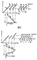
- the device of FIG. 1 can be used in suitably designed circuitry for a variety of functions; one circuit, designed for frequency multiplication, is shown in FIG. 7 with associated current-voltage diagrams of FIG. 8 and FIG. 9, bias voltage V BA between terminal A and B of the device being fixed.
- FIG. 8 shows device characteristics in the case of a sawtooth input voltage, substrate bias voltage V SS having been adjusted to select the quiescent operating point A2.
- the sawtooth input voltage increases from A1 to B1
- the operating point shifts from A2 to B2 along the characteristic, with the substrate current I s increasing approximately linearly.
- the output voltage across the resistance R is proportional to the source current I s , and thus its increase from A3 to B3 is also approximately linear.
- the source current I s suddenly drops to the valley point B2′, resulting in a sudden drop in the output voltage from B3 to B3′.
- the output continues to rise again, followed by a second drop at C2, and then a rise as the input continues to rise up to D1.
- the input returns to zero to start a new cycle, and the operating point also shifts back to A2, with a drop in the output as well. Accordingly, the frequency of the sawtooth input signal has been multiplied by a factor of 3. (If V BA had been adjusted to produce a single peak in the current-voltage diagram, sawtooth frequency would have been multiplied by a factor of two.)
- FIG. 9 illustrates device operation in case of a sine-wave input and is amenable to detailed description analogous to description in the case of FIG. 8 above.
- the output waveform is found to be rich in the fifth harmonic of the input. (If V BA had been adjusted to produce a single peak in the current-voltage diagram, the output would have been rich in the third harmonic.)
- FIG. 10 shows output of a circuit of FIG. 7 used for waveform scrambling in the case of a sine-wave input signal.
- the original waveform can be recovered from the scrambled signal by using an identical device in the feedback circuit of an amplifier, biased to the same voltages as in the scrambling circuit.
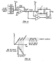
- FIG. 11 shows a circuit which can serve as a memory element in a 3-state logic system. Shown are source 91 of supply voltage V SS , source 92 of bias voltage V BA , input signal source 93, resistor 94, and output terminal 95. As illustrated in FIG. 12, the bias voltage V BA between the terminals A and B is adjusted to produce a current-voltage characteristic having essentially equal peaks at the same current level. And, for a suitable supply voltage V SS , and load resistance R L , the load line intersects the current-voltage characteristic at five different points of which three (Q1, Q2, and Q3) are in the positive slope parts of the curve and hence correspond to stable operating points.
- the circuit can stay indefinitely at any one of these points, thus retaining the last voltage information supplied.
- the device can be used as a memory element having three stable states, with voltages V1, V2, and V3 representing three logic values. (As compared with existing three-state logic circuits requiring 4 conventional transistors and 6 resistors, this represents a significantly simpler alternative.)
- the circuit can be switched from one state to another by applying a short voltage pulse.
- the three-state memory cell as discussed above in connection with FIG. 11 and FIG. 12 is well-suited for integration in memory integrated circuits with read-write and encoding capabilities as shown in FIG. 13.
- the memory cells are interconnected as a matrix array, and a particular element in the array is addressed by activating the corresponding row- and column-select lines.
- a row-select connects each device in a specified row to the corresponding column line, and the column-select connects the selected column to the data bus.
- the driving switch Q1 is turned on, as well as the switches for every element in the i-th row.
- the column-select logic now connects the j-th column to the data bus.
- the ternary identity cell T (described in detail, e.g., by A. Heung et al., "An all-CMOS Ternary Identity Cell for VLSI Implementation", Electronics Letters, Vol. 20 (1984), pp. 221-222) acts as buffer between the memory element and the external circuit.
- the identity cell For reading data from the memory, the identity cell is activated with the read-enable line, and data from the (i, j)-th element is transferred via the data bus to the I/O pin of the circuit.
- the write-enable line When the write-enable line is activated, data from an external circuit is connected to the data bus and written on the (i, j)-th element.
- FIG. 14 shows a circuit which can operate as a 4-bit parity generator, appreciation of corresponding device operation being facilitated by reference to FIG. 15 which shows the current-voltage characteristic of the device.
- the four digital input signals are added in the inverting summing amplifier A1 to produce five distinct voltage steps at its output, corresponding to the number of digital bits in the high state. Normally, the output of A1 would be negative for positive input voltages.
- the addition of a suitable negative offset voltage V OFF at the input results in up-shifting of the waveform to produce the output for A1 shown in the bottom part of FIG. 15.
- the substrate bias voltage V SS is adjusted to select the operating points of the device at the five points emphasized by dots in the current-voltage characteristic, corresponding, respectively, to the five voltage levels at the A1 output.
- the substrate current of the device generates a voltage across the 7.5-ohm resistor, which is picked up by the buffer amplifier A2.
- the circuit operates as a 4-bit parity generator in that its output is high when the number of input bits set high is odd, and low otherwise. As compared with a conventional circuit using 3 exclusive-OR gates, each requiring 8 transistors, considerable reduction in the number of circuit components is realized in the circuit of FIG. 14.
- circuits of FIG. 7, 11, 13, and 14 preferably involves the use of highly miniaturized resonant-tunneling devices
- relatively large-scale devices having dimensions as described with respect to FIG.1 are of immediate interest on account of low internal impedance of approximately 10 ohms, and further on account of compatibility with bipolar threshold detectors due to voltage steps of approximately 0.6 to 0.7 volts.
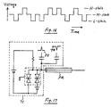
- a device as described can be used as a driver of the pseudo-ternary signal used in coaxial-cable telephone transmission; see FIG. 16 for a typical such signal stream as designed for easy extraction of the clock signal.
- FIG. 17 diagrammatically shows pseudo-ternary driver 71 for coaxial cable 72; driver 71 includes device 1 in accordance with FIG. 1.
- internal impedance of driver 71 is less than approximately one-tenth of the characteristic impedance of cable 72, the latter typically being in the range from 50 to 75 ohms.
- the driver is at the middle state (M-state). If an up-going pulse 73 is applied, the driver undergoes transition to the high state (H-state), and if then a down-going pulse 74 is applied, the driver returns to the middle state. With the driver at middle state, if a down-going pulse 74 is applied, the driver switches to the low state (L-state).
- a two-terminal device is of interest as exemplified by a device made by molecular-beam epitaxy processing as follows:
- n+ indium phosphide substrate On an n+ indium phosphide substrate a one-micrometer buffer layer was grown of n+ (approximately 3 x 10¹⁷/cm3) Ga 0.47 In 0.53 As, followed by a resonant-tunneling structure consisting of three 5-nanometer layers such as a first barrier layer of undoped Al 0.48 In 0.52 As, a quantum well layer of undoped Ga 0.47 In 0.53 As, and a second barrier layer of undoped Al 0.48 In 0.52 As. On the resonant-tunneling structure, a 1-micrometer cap layer of n+ (approximately 3 x 10¹⁷/cm3) Ga 0.47 In 0.53 As was deposited.
- a 50-micrometer mesa structure was formed by etching with 1 H2O2 + 3 H3PO4 + 50 H2O at room temperature, and a top ohmic contact having a diameter of 30 micrometers was made by sequential deposition of 6 nanometers germanium, 13.5 nanometers gold, 50 nanometers silver, and 75 nanometers gold, and alloying at a temperature of 420 degrees C for 30 seconds.
- a top ohmic contact having a diameter of 30 micrometers was made by sequential deposition of 6 nanometers germanium, 13.5 nanometers gold, 50 nanometers silver, and 75 nanometers gold, and alloying at a temperature of 420 degrees C for 30 seconds.
- For the bottom contact 5 nanometers nickel, 38.5 nanometers gold, 21.5 nanometers germanium, and 75 nanometers gold were deposited on the etched surface of the buffer layer and alloyed at a temperature of 420 degrees C for 30 seconds.
- Diode operation was tested at a temperature of 80 degrees K and at room temperature in a Helitran dewar equipped with microprobes. Resulting current-voltage characteristic are as shown in FIG. 18 and FIG. 19, respectively, bias voltage being defined as voltage of the top contact relative to the bottom contact.
- room-temperature operation exhibits a peak-to-valley ratio of 4 : 1 in one polarity, and 3.5 : 1 in the other. While the peak-to-valley ratio increases upon cooling of the device, peak current remains essentially constant (approximately 125 mA at 600 mV).
- a resonant-tunneling diode as described above is suitable for operation at temperatures greater than 100 degrees K and, in particular, at temperatures at or near room temperature.
- resonant-tunneling diodes are suitable for a variety of circuit applications.
- a circuit consisting of a voltage source, a resonant-tunneling diode, and a load resistor in series can serve as a bistable memory cell as may be implemented, e.g., by replacing device 1 in FIG. 13 by a resonant-tunneling diode.
- the diode as described above exhibits abrupt current drop. While this device aspect is desirable, e.g., for memory application, other device uses such as, e.g., analog applications may preferably be based on characteristics having a region of more gradual current transition.
- a device of this latter kind has been realized as follows: on the emitter side of the device, an essentially undoped layer is interposed between the contact and the first barrier layer to permit, during device operation, emitted carriers to be accelerated in the electric field in the undoped layer. As a result, carrier energy at the barrier can be described by a distribution as depicted in the diagram of FIG. 20, with a peak occurring at an energy substantially higher than the conduction band edge.
- preferred accelerator layer thickness is greater than or equal to 40 nanometers.
- Shown in FIG. 21 is the current-voltage characteristic of a corresponding device having the following spcific structure on an indium phosphide substrate: 500 nanometers N+ Ga 0.47 In 0.53 As, 5 nanometers undoped Al 0.48 In 0.52 As, 5 nanometers undoped Ga 0.47 In 0.53 As, 5 nanometers undoped Al 0.48 In 0.52 As, 200 nanometers undoped Ga 0.47 In 0.53 As, and 200 nanometers n+ Ga 0.47 In 0.53 As.
Landscapes
- Engineering & Computer Science (AREA)
- Computer Hardware Design (AREA)
- Chemical & Material Sciences (AREA)
- Nanotechnology (AREA)
- Physics & Mathematics (AREA)
- Mathematical Physics (AREA)
- Theoretical Computer Science (AREA)
- Crystallography & Structural Chemistry (AREA)
- Semiconductor Memories (AREA)
- Static Random-Access Memory (AREA)
- Bipolar Transistors (AREA)
- Junction Field-Effect Transistors (AREA)
Applications Claiming Priority (2)
| Application Number | Priority Date | Filing Date | Title |
|---|---|---|---|
| US117583 | 1987-11-05 | ||
| US07/117,583 US4853753A (en) | 1987-07-01 | 1987-11-05 | Resonant-tunneling device, and mode of device operation |
Publications (2)
| Publication Number | Publication Date |
|---|---|
| EP0320110A2 true EP0320110A2 (fr) | 1989-06-14 |
| EP0320110A3 EP0320110A3 (fr) | 1990-05-09 |
Family
ID=22373703
Family Applications (1)
| Application Number | Title | Priority Date | Filing Date |
|---|---|---|---|
| EP88310336A Ceased EP0320110A3 (fr) | 1987-11-05 | 1988-11-03 | Dispositif de mémoire comprenant une diode semi-conductrice à effet tunnel résonnant et mode opératoire |
Country Status (5)
| Country | Link |
|---|---|
| US (1) | US4853753A (fr) |
| EP (1) | EP0320110A3 (fr) |
| JP (1) | JPH023142A (fr) |
| KR (1) | KR930002817B1 (fr) |
| CA (1) | CA1282871C (fr) |
Cited By (2)
| Publication number | Priority date | Publication date | Assignee | Title |
|---|---|---|---|---|
| EP0297778A3 (fr) * | 1987-07-01 | 1991-04-03 | AT&T Corp. | Appareil comprenant un dispositif à effet tunnel résonnant ayant des caractéristiques courant/tension à plusieurs pointes |
| EP0708487A1 (fr) * | 1994-10-20 | 1996-04-24 | Hitachi Europe Limited | Dispositif de mémoire |
Families Citing this family (14)
| Publication number | Priority date | Publication date | Assignee | Title |
|---|---|---|---|---|
| US4926232A (en) * | 1987-09-02 | 1990-05-15 | Nec Corporation | Resonant-tunneling bipolar transistor |
| US5012301A (en) * | 1990-02-22 | 1991-04-30 | Northern Telecom Limited | Three terminal semiconductor device |
| US4999687A (en) * | 1990-04-25 | 1991-03-12 | At&T Bell Laboratories | Logic element and article comprising the element |
| US5128894A (en) * | 1990-09-28 | 1992-07-07 | University Of Maryland | Multi-value memory cell using resonant tunnelling diodes |
| US5126553A (en) * | 1990-11-28 | 1992-06-30 | Bell Communications Research, Inc. | Bistable optically switchable resonant-tunneling device and its use in signal processing |
| US5347140A (en) * | 1991-08-27 | 1994-09-13 | Matsushita Electric Industrial Co., Ltd. | Resonant electron transfer device |
| US5237596A (en) * | 1991-10-08 | 1993-08-17 | University Of Maryland | Stepping counter using resonant tunneling diodes |
| JP3542620B2 (ja) * | 1992-09-30 | 2004-07-14 | テキサス インスツルメンツ インコーポレイテツド | 多重ピーク共鳴トンネルダイオード |
| US5408107A (en) * | 1993-05-20 | 1995-04-18 | The Board Of Regents Of The University Of Texas System | Semiconductor device apparatus having multiple current-voltage curves and zero-bias memory |
| US5539214A (en) * | 1995-02-06 | 1996-07-23 | Regents Of The University Of California | Quantum bridges fabricated by selective etching of superlattice structures |
| JP2001077352A (ja) * | 1999-09-07 | 2001-03-23 | Sony Corp | 半導体素子およびその製造方法 |
| US8368380B2 (en) * | 2010-03-31 | 2013-02-05 | General Electric Company | Devices and methods for electric field sensing |
| US8604772B2 (en) * | 2010-03-31 | 2013-12-10 | General Electric Company | MEMS-based resonant tunneling devices and arrays of such devices for electric field sensing |
| WO2023062601A1 (fr) * | 2021-10-15 | 2023-04-20 | 6Gco Ltd. | Ordinateur non binaire utilisant un courant alternatif |
Family Cites Families (5)
| Publication number | Priority date | Publication date | Assignee | Title |
|---|---|---|---|---|
| GB984222A (en) * | 1961-04-13 | 1965-02-24 | Nat Res Dev | Negative resistance diode storage circuits |
| US4410902A (en) * | 1981-03-23 | 1983-10-18 | The United States Of America As Represented By The Secretary Of The Army | Planar doped barrier semiconductor device |
| JPS6150359A (ja) * | 1984-08-20 | 1986-03-12 | Fujitsu Ltd | 半導体記憶装置 |
| JPS61161774A (ja) * | 1985-01-10 | 1986-07-22 | Nec Corp | ダイオ−ド |
| US4667211A (en) * | 1985-09-05 | 1987-05-19 | The United States Of America As Represented By The Secretary Of The Army | Millimeter wave-infrared bloch oscillator/detector |
-
1987
- 1987-11-05 US US07/117,583 patent/US4853753A/en not_active Expired - Fee Related
-
1988
- 1988-11-02 KR KR1019880014355A patent/KR930002817B1/ko not_active Expired - Fee Related
- 1988-11-03 EP EP88310336A patent/EP0320110A3/fr not_active Ceased
- 1988-11-04 JP JP63277613A patent/JPH023142A/ja active Pending
- 1988-11-04 CA CA000582271A patent/CA1282871C/fr not_active Expired - Fee Related
Cited By (4)
| Publication number | Priority date | Publication date | Assignee | Title |
|---|---|---|---|---|
| EP0297778A3 (fr) * | 1987-07-01 | 1991-04-03 | AT&T Corp. | Appareil comprenant un dispositif à effet tunnel résonnant ayant des caractéristiques courant/tension à plusieurs pointes |
| EP0708487A1 (fr) * | 1994-10-20 | 1996-04-24 | Hitachi Europe Limited | Dispositif de mémoire |
| US5811832A (en) * | 1994-10-20 | 1998-09-22 | Hitachi, Ltd. | Non-volatile memory device |
| US6194303B1 (en) | 1994-10-20 | 2001-02-27 | Hitachi, Ltd. | Memory device |
Also Published As
| Publication number | Publication date |
|---|---|
| JPH023142A (ja) | 1990-01-08 |
| KR890009006A (ko) | 1989-07-13 |
| EP0320110A3 (fr) | 1990-05-09 |
| KR930002817B1 (ko) | 1993-04-10 |
| CA1282871C (fr) | 1991-04-09 |
| US4853753A (en) | 1989-08-01 |
Similar Documents
| Publication | Publication Date | Title |
|---|---|---|
| Capasso et al. | Quantum functional devices: resonant-tunneling transistors, circuits with reduced complexity, and multiple valued logic | |
| Sen et al. | Resonant tunneling device with multiple negative differential resistance: digital and signal processing applications with reduced circuit complexity | |
| US5151618A (en) | Resonant-tunneling heterojunction bipolar transistor device | |
| US4902912A (en) | Apparatus including resonant-tunneling device having multiple-peak current-voltage characteristics | |
| US5021841A (en) | Semiconductor device with controlled negative differential resistance characteristic | |
| US4853753A (en) | Resonant-tunneling device, and mode of device operation | |
| US5023836A (en) | Semiconductor memory device | |
| Capasso et al. | Resonant tunneling devices with multiple negative differential resistance and demonstration of a three-state memory cell for multiple-valued logic applications | |
| CA1276275C (fr) | Transistor a effet tunnel resonant | |
| JPH02231777A (ja) | 共鳴トンネル光電素子 | |
| US4959696A (en) | Three terminal tunneling device and method | |
| US6303941B1 (en) | Integrated asymmetric resonant tunneling diode pair circuit | |
| US4999697A (en) | Sequential-quenching resonant-tunneling transistor | |
| JP2746771B2 (ja) | 半導体装置 | |
| US4182965A (en) | Semiconductor device having two intersecting sub-diodes and transistor-like properties | |
| EP0297778A2 (fr) | Appareil comprenant un dispositif à effet tunnel résonnant ayant des caractéristiques courant/tension à plusieurs pointes | |
| Beresford et al. | Resonant interband tunneling device with multiple negative differential resistance regions | |
| EP0363238A2 (fr) | Dispositif semi-conducteur à effet quantique ayant des propriétés de résistance différentielle négative | |
| EP0698925A2 (fr) | Transistor bipolaire à base flottante | |
| JPH09162394A (ja) | トンネルトランジスタ及び記憶回路 | |
| Capasso et al. | Quantum transistors and circuits break through the barriers | |
| CHO | AND ALFRED zyxwvutsrqponmlkjih | |
| Tehrani et al. | Three terminal quantum structure based on resonant interband tunneling | |
| JPH0831591B2 (ja) | 高速半導体装置 | |
| BABA et al. | Surface tunnel transistors with multiple interband tunnel junctions |
Legal Events
| Date | Code | Title | Description |
|---|---|---|---|
| PUAI | Public reference made under article 153(3) epc to a published international application that has entered the european phase |
Free format text: ORIGINAL CODE: 0009012 |
|
| AK | Designated contracting states |
Kind code of ref document: A2 Designated state(s): DE ES FR GB NL |
|
| PUAL | Search report despatched |
Free format text: ORIGINAL CODE: 0009013 |
|
| AK | Designated contracting states |
Kind code of ref document: A3 Designated state(s): DE ES FR GB NL |
|
| 17P | Request for examination filed |
Effective date: 19901030 |
|
| 17Q | First examination report despatched |
Effective date: 19920721 |
|
| STAA | Information on the status of an ep patent application or granted ep patent |
Free format text: STATUS: THE APPLICATION HAS BEEN REFUSED |
|
| RAP3 | Party data changed (applicant data changed or rights of an application transferred) |
Owner name: AT&T CORP. |
|
| 18R | Application refused |
Effective date: 19940218 |