EP0320660A2 - Integrierte Schaltungspackung - Google Patents
Integrierte Schaltungspackung Download PDFInfo
- Publication number
- EP0320660A2 EP0320660A2 EP88119363A EP88119363A EP0320660A2 EP 0320660 A2 EP0320660 A2 EP 0320660A2 EP 88119363 A EP88119363 A EP 88119363A EP 88119363 A EP88119363 A EP 88119363A EP 0320660 A2 EP0320660 A2 EP 0320660A2
- Authority
- EP
- European Patent Office
- Prior art keywords
- wafer
- substrate
- strips
- lines
- semiconductor wafer
- Prior art date
- Legal status (The legal status is an assumption and is not a legal conclusion. Google has not performed a legal analysis and makes no representation as to the accuracy of the status listed.)
- Granted
Links
Images



Classifications
-
- H—ELECTRICITY
- H10—SEMICONDUCTOR DEVICES; ELECTRIC SOLID-STATE DEVICES NOT OTHERWISE PROVIDED FOR
- H10P—GENERIC PROCESSES OR APPARATUS FOR THE MANUFACTURE OR TREATMENT OF DEVICES COVERED BY CLASS H10
- H10P72/00—Handling or holding of wafers, substrates or devices during manufacture or treatment thereof
- H10P72/04—Apparatus for manufacture or treatment
- H10P72/0438—Apparatus for making assemblies not otherwise provided for, e.g. package constructions
-
- G—PHYSICS
- G01—MEASURING; TESTING
- G01R—MEASURING ELECTRIC VARIABLES; MEASURING MAGNETIC VARIABLES
- G01R1/00—Details of instruments or arrangements of the types included in groups G01R5/00 - G01R13/00 and G01R31/00
- G01R1/02—General constructional details
- G01R1/04—Housings; Supporting members; Arrangements of terminals
- G01R1/0408—Test fixtures or contact fields; Connectors or connecting adaptors; Test clips; Test sockets
- G01R1/0491—Test fixtures or contact fields; Connectors or connecting adaptors; Test clips; Test sockets for testing integrated circuits on wafers, e.g. wafer-level test cartridge
-
- H—ELECTRICITY
- H10—SEMICONDUCTOR DEVICES; ELECTRIC SOLID-STATE DEVICES NOT OTHERWISE PROVIDED FOR
- H10W—GENERIC PACKAGES, INTERCONNECTIONS, CONNECTORS OR OTHER CONSTRUCTIONAL DETAILS OF DEVICES COVERED BY CLASS H10
- H10W78/00—Detachable holders for supporting packaged chips in operation
Definitions
- This invention relates generally to the packaging of semiconductor devices for use in computers, and more particularly to packaging of full wafers of silicon having integrated circuit devices formed thereon.
- the invention as claimed is intended to remedy these drawbacks. It solves the problem of providing an improved full wafer package which has improved power delivery and distribution characteristics as well as improved thermal cooling and a good thermal match between the wafer and the substrate.
- the package includes a substrate which mounts a semiconductor wafer on at least one side thereof. The wafer and substrate are thermally matched for coefficient of expansion.
- the wafer has integrated circuit devices formed thereon and current carrying lines on the surface of the wafer interconnect the devices to each other to form integrated circuits. Electrical conducting buses are provided comprised of electrically conducting strips which extend transversally across the surface of the wafer and are connected to appropriate current carrying lines on the wafer surface.
- the strips are connected to desired voltage levels to thus provide the correct voltage level directly on the surface of the wafer and thereby provide improved voltage and signal response characteristics to the circuit components.
- the invention also contemplates packing the wafer-substrate device inside a heat sink cover member and packing a solid conformable thermally conducting material between the cover and wafer, and providing adjustable fastening means to secure the substrate and wafer to the cover and allow adjustment of the cover with respect to the wafer for the purpose of improving contact of the cover and wafer with the thermally conducting solid material.
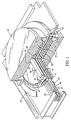
- a substrate 10 is provided, which mounts silicon wafers 12 on both sides thereof, the wafers preferably being secured to the substrate by solder connections 14.
- the wafers 12 have various semicondutor devices formed on their surfaces and extending down therein and interconnected by lines of conducting material 15 to form integrated circuits. Such wafers having these integrated circuits are well known in the art, e.g. see U.S. Patent 3,999,105.
- the substrate material is preferably made of copper clad Invar, and either lead-tin or lead-indium solder is preferred.
- One of the important aspects of this invention is the requirement for the thermal coefficients of expansion of the substrate and the silicon wafer be matched since if there is any significant mismatch, cracking and other failure of wafers can occur. Further, the matching does not constitute selecting the substrate to have the same coefficient of thermal expansion as the wafer for the following reasons.
- the operating semiconductor devices are located at or near the top of the silicon wafer, and hence when operating, generate power which causes a temperature rise at the top surface of the silicon wafer.
- the heat transfer through the wafer 12 and the solder 14 to the substrate 10 involves the loss of heat and thus the surface of the substrate 10 will be at a lower temperature than the surface of the silicon wafer 12.
- the surface of the silicon wafer may be at a temperature of 85°C during operation of the device, whereas the surface of the substrate may be at about 75°C.
- the substrate must have a proportionately higher coefficient of expansion than that of the silicon wafer.
- the difference in coefficient of expansion of the wafer and the sustrate should be in the ratio of the temperature rise of the wafer to the temperature rise of the substrate from ambient (i.e. normal non-operating temperature of the wafer and substrate) to the average operating temperature of the wafer.
- the ratio of coefficient of thermal expansion of the substrate to the coefficient of thermal expansion of the wafer would be 85-20/75-20 or 65/55 or 1.18.
- the substrate should have a coefficient of expansion of about 3.54 ppm/°C (3.0 x 1.18).
- TCE sub coefficient of thermal expansion of the substrate material
- TCE waf coefficient of thermal expansion of wafer material
- T waf average operating surface temperature of wafer
- T sub average operating surface temperature of substrates
- T AMB ambient temperature
- the TCE of silicon wafer varies with different dopants and other factors, which are known, and the TCE of the wafer can be easily and routinely determined. This can be done by constructing an operating model, or can be calculated based on known thermal resistance of the wafer and the thickness of wafer. It is also well known in the art that the TCE of copper clad Invar can be varied by varying the thickness of the copper coating. Thus routine calculation and/or temperature measurements will provide the necessary values to select the proper substrate for the required thermal substrate.
- the devices on the silicon substrate are connected to pads 16 located around the periphery thereof, which pads 16 are connected to corresponding connectors 18 arranged around the periphery of the substrate 10 by means of wire leads 20.
- These connections are preferably formed by laser welding of the wire leads to both the pads 16 and 18, and can be done by using a decal technique, wherein the wires are supported in a predetermined array and then laser welded.
- the wafers are provided with two sets of power voltage lines 22 and 24, the lines 22 being adapted to bring desired operating voltage levels to the devices, and the lines 24 being designed to provide a ground voltage to the devices.
- ground voltage may be applied by utilizing the substrate material, and the lines 22 and 24 can be used for different voltage levels.
- An electrically conducting bus 26 extends transversely across the wafer and is comprised of a voltage section 28 and a ground section 30 joined by a dielectric material 32.
- the bus is configured to have contact with the wafer 12 on its face, and the voltage section 28 is connected to the voltage lines 22 by solder connection and the ground section 30 is connected to the ground lines 24 also by solder connections.
- the necessary conductor size can be easily achieved, and voltage supplied at all points across the wafer without being tied to the necessity of bringing in voltage on small size metallurgy conductors from the edge.
- a plurality of additional buses parallel to the bus 26 can be used, as electrical requirements dictate, with the sections of the busses being connected to appropriate voltage and ground conductors on the wafer surface.
- a second advantage of this arrangement is that the voltage source is brought closer to the devices, and this can be significant in CMOS technology which requires rapid response time for device drivers, this being achieved by the closer proximity of the voltage source.
- the voltage section 28 has a lead 34 connected to a voltage source, and the ground section 30 has a lead 36 connected to ground.
- a 3 or 4 part single bus, or multiple busses could be used if more than two voltage levels are desired.
- Two types of three part single busses are shown in Figure 9 and 10.
- a bus 25a is shown comprised of a pair of voltage sections 27a and 29a and a ground section 31a all encapsulated in a dielectric material 32a.
- the voltage section 27a and 29a and ground section 31a are preferably formed of invar clad copper and are matched to the coefficient of thermal expansion of the wafer in the same manner as previously described with respect to matching the thermal expansion of the wafer to tbe substrate.
- the bus is face connected to voltage lines 21a and 23a and ground lines 24a by means of solder connection 33a. In this case two different voltage levels in addition to ground can be achieved.
- Figure 10 is similar to Figure 9, except that it is an edge connection configuration in which a bus 25b is comprised of a pair of voltage lines 27b and 29b and a ground section 31b, all encapsulated in a dielectric material 32b. Again the voltage lines 27b and 29b and ground section 31b are formed of Invar clad copper with their thermal coefficients of expansion matched to the wafer as previously described.
- the bus is edge connected to voltage lines 21b and 23b and ground line 24b by solder connection 33b, but in this case it is an edge configured connection.
- a heat sink cover member 38 is provided comprised of a pair of identical mating sections 40 enclosing the mounted wafers. Each section 40 has flanges 42 around the outer edge thereof.
- a disk shaped sheet of elastomeric thermally conducting solid compliable material 44 is disposed between each wafer and its respective section 40 of the heat sink cover to provide a thermal conduction path.
- One such material is a mixture of (by weight) about 100 parts silicon gum, about 500 parts zirconium silicate, and about 6 parts of a wetting agent sold by General Electric under the trademark VISCASEL 600M. This provides the desired properties of good thermal conductivity and thermal stability, and deformation resistance.
- a ring of elastomeric sealing material 46 is provided around each of the flanges of the covers between the flange and substrate 10, and circumferentially spaced bolts and nuts 48 and 50 resiliantly secure the cover sections 40 together and to the substrate.
- each cover section 40 has a slot 52 in which the bus 26 is disposed. (Of course, if there is more than one bus, a slot for each will be provided.)
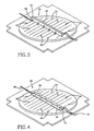
- FIGS 2 and 3 show a somewhat modified form of the bus structure of the invention.
- a bus 56 is formed of voltage section 58 and ground section 60 joined in face-to-face relationship by dielectric adhesive 62.
- This bus structure is configured to be maintained with its edge contacting the wafer 12 as shown in Figure 3 rather than its face as previously described.
- a slot 64 in each of the cover structures 40 is provided in which the bus is disposed.
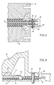
- FIG. 7 and 8 A modification of the invention is shown in Figure 7 and 8.
- an elastomeric solid conformable dielectric thermally conducting material 70 is provided, which is cut or otherwise formed to substantially conform to the entire space between the wafer 12, including the pads 16 as well as the space around the wafer, between the substrate and the cover member 38.
- This can be the same type of thermally conducting material as previously described.
- the material 70 as shown has a central essentially uniformly thick center section 72 overlaying the wafer and a shaped outer portion 74 disposed in and around the location of the electrical signal connections to the pads 16 and 18.
Landscapes
- Engineering & Computer Science (AREA)
- Computer Hardware Design (AREA)
- Microelectronics & Electronic Packaging (AREA)
- Physics & Mathematics (AREA)
- General Physics & Mathematics (AREA)
- Cooling Or The Like Of Semiconductors Or Solid State Devices (AREA)
- Wire Bonding (AREA)
- Semiconductor Integrated Circuits (AREA)
- Design And Manufacture Of Integrated Circuits (AREA)
Applications Claiming Priority (2)
| Application Number | Priority Date | Filing Date | Title |
|---|---|---|---|
| US07/134,480 US4899208A (en) | 1987-12-17 | 1987-12-17 | Power distribution for full wafer package |
| US134480 | 1998-08-13 |
Publications (3)
| Publication Number | Publication Date |
|---|---|
| EP0320660A2 true EP0320660A2 (de) | 1989-06-21 |
| EP0320660A3 EP0320660A3 (en) | 1989-08-09 |
| EP0320660B1 EP0320660B1 (de) | 1994-02-16 |
Family
ID=22463586
Family Applications (1)
| Application Number | Title | Priority Date | Filing Date |
|---|---|---|---|
| EP88119363A Expired - Lifetime EP0320660B1 (de) | 1987-12-17 | 1988-11-22 | Integrierte Schaltungspackung |
Country Status (4)
| Country | Link |
|---|---|
| US (1) | US4899208A (de) |
| EP (1) | EP0320660B1 (de) |
| JP (1) | JPH01173627A (de) |
| DE (1) | DE3887849T2 (de) |
Cited By (11)
| Publication number | Priority date | Publication date | Assignee | Title |
|---|---|---|---|---|
| US5150196A (en) * | 1989-07-17 | 1992-09-22 | Hughes Aircraft Company | Hermetic sealing of wafer scale integrated wafer |
| WO1998018302A1 (en) * | 1996-10-21 | 1998-04-30 | Telefonaktiebolaget Lm Ericsson (Publ) | Means and method for mounting electronics |
| WO1998024124A1 (de) * | 1996-11-26 | 1998-06-04 | Siemens Aktiengesellschaft | Sockel für integrierte schaltung |
| EP2772768A1 (de) * | 2007-04-05 | 2014-09-03 | AEHR Test Systems | Elektronischer Tester mit Signalverteiler und Waferfutter mit verschiedenen Wärmeausdehnungskoeffizienten |
| US11448695B2 (en) | 2007-12-19 | 2022-09-20 | Aehr Test Systems | System for testing an integrated circuit of a device and its method of use |
| US11592465B2 (en) | 2009-03-25 | 2023-02-28 | Aehr Test Systems | Pressure relief valve |
| US11635459B2 (en) | 2017-03-03 | 2023-04-25 | Aehr Test Systems | Electronics tester |
| US11835575B2 (en) | 2020-10-07 | 2023-12-05 | Aehr Test Systems | Electronics tester |
| US11860221B2 (en) | 2005-04-27 | 2024-01-02 | Aehr Test Systems | Apparatus for testing electronic devices |
| US12007451B2 (en) | 2016-01-08 | 2024-06-11 | Aehr Test Systems | Method and system for thermal control of devices in an electronics tester |
| US12584958B2 (en) | 2022-12-30 | 2026-03-24 | Aehr Test Systems | Electronics tester |
Families Citing this family (10)
| Publication number | Priority date | Publication date | Assignee | Title |
|---|---|---|---|---|
| US5038201A (en) * | 1988-11-08 | 1991-08-06 | Westinghouse Electric Corp. | Wafer scale integrated circuit apparatus |
| JPH02267947A (ja) * | 1989-04-07 | 1990-11-01 | Mitsubishi Electric Corp | 半導体装置 |
| US5412247A (en) * | 1989-07-28 | 1995-05-02 | The Charles Stark Draper Laboratory, Inc. | Protection and packaging system for semiconductor devices |
| US5223741A (en) * | 1989-09-01 | 1993-06-29 | Tactical Fabs, Inc. | Package for an integrated circuit structure |
| US5068715A (en) * | 1990-06-29 | 1991-11-26 | Digital Equipment Corporation | High-power, high-performance integrated circuit chip package |
| EP0514615B1 (de) * | 1991-05-23 | 1995-05-03 | STMicroelectronics S.r.l. | Elektronische Leistungsanordnung realisiert durch eine Reihe elementarer Halbleiterbauelemente in Parallelverbindung und verwandtes Herstellungsverfahren |
| US5285108A (en) * | 1991-06-21 | 1994-02-08 | Compaq Computer Corporation | Cooling system for integrated circuits |
| US6233184B1 (en) | 1998-11-13 | 2001-05-15 | International Business Machines Corporation | Structures for wafer level test and burn-in |
| JP2007202382A (ja) * | 2005-12-28 | 2007-08-09 | Mabuchi Motor Co Ltd | 小型モータの光学式エンコーダ装置及びその製造方法 |
| JP4857785B2 (ja) * | 2006-01-27 | 2012-01-18 | ミツミ電機株式会社 | エンコーダ付モータ及びその組立方法 |
Family Cites Families (11)
| Publication number | Priority date | Publication date | Assignee | Title |
|---|---|---|---|---|
| US3999105A (en) * | 1974-04-19 | 1976-12-21 | International Business Machines Corporation | Liquid encapsulated integrated circuit package |
| US4000509A (en) * | 1975-03-31 | 1976-12-28 | International Business Machines Corporation | High density air cooled wafer package having improved thermal dissipation |
| US4025997A (en) * | 1975-12-23 | 1977-05-31 | International Telephone & Telegraph Corporation | Ceramic mounting and heat sink device |
| JPS5471572A (en) * | 1977-11-18 | 1979-06-08 | Fujitsu Ltd | Semiconductor device |
| US4549200A (en) * | 1982-07-08 | 1985-10-22 | International Business Machines Corporation | Repairable multi-level overlay system for semiconductor device |
| JPS6074554A (ja) * | 1983-09-30 | 1985-04-26 | Fujitsu Ltd | 大規模集積回路 |
| US4595945A (en) * | 1983-10-21 | 1986-06-17 | At&T Bell Laboratories | Plastic package with lead frame crossunder |
| JPS60177656A (ja) * | 1984-02-24 | 1985-09-11 | Hitachi Micro Comput Eng Ltd | 半導体装置 |
| US4672421A (en) * | 1984-04-02 | 1987-06-09 | Motorola, Inc. | Semiconductor packaging and method |
| JPS625649A (ja) * | 1985-07-01 | 1987-01-12 | Nec Ic Microcomput Syst Ltd | 集積回路パツケ−ジ |
| AU598253B2 (en) * | 1986-05-07 | 1990-06-21 | Digital Equipment Corporation | System for detachably mounting semi-conductors on conductor substrates |
-
1987
- 1987-12-17 US US07/134,480 patent/US4899208A/en not_active Expired - Fee Related
-
1988
- 1988-10-12 JP JP63255066A patent/JPH01173627A/ja active Granted
- 1988-11-22 EP EP88119363A patent/EP0320660B1/de not_active Expired - Lifetime
- 1988-11-22 DE DE3887849T patent/DE3887849T2/de not_active Expired - Fee Related
Cited By (29)
| Publication number | Priority date | Publication date | Assignee | Title |
|---|---|---|---|---|
| US5150196A (en) * | 1989-07-17 | 1992-09-22 | Hughes Aircraft Company | Hermetic sealing of wafer scale integrated wafer |
| WO1998018302A1 (en) * | 1996-10-21 | 1998-04-30 | Telefonaktiebolaget Lm Ericsson (Publ) | Means and method for mounting electronics |
| US6108205A (en) * | 1996-10-21 | 2000-08-22 | Telefonaktiebolaget Lm Ericsson | Means and method for mounting electronics |
| WO1998024124A1 (de) * | 1996-11-26 | 1998-06-04 | Siemens Aktiengesellschaft | Sockel für integrierte schaltung |
| US12163999B2 (en) | 2005-04-27 | 2024-12-10 | Aehr Test Systems | Apparatus for testing electronic devices |
| US11860221B2 (en) | 2005-04-27 | 2024-01-02 | Aehr Test Systems | Apparatus for testing electronic devices |
| US10976362B2 (en) | 2007-04-05 | 2021-04-13 | Aehr Test Systems | Electronics tester with power saving state |
| US9857418B2 (en) | 2007-04-05 | 2018-01-02 | Aehr Test Systems | Electronics tester with group and individual current configurations |
| US10151793B2 (en) | 2007-04-05 | 2018-12-11 | Aehr Test Systems | Electronics tester with double-spiral thermal control passage in a thermal chuck |
| US10718808B2 (en) | 2007-04-05 | 2020-07-21 | Aehr Test Systems | Electronics tester with current amplification |
| EP2772768A1 (de) * | 2007-04-05 | 2014-09-03 | AEHR Test Systems | Elektronischer Tester mit Signalverteiler und Waferfutter mit verschiedenen Wärmeausdehnungskoeffizienten |
| US9291668B2 (en) | 2007-04-05 | 2016-03-22 | Aehr Test Systems | Electronics tester with a valve integrally formed in a component of a portable pack |
| US9500702B2 (en) | 2007-04-05 | 2016-11-22 | Aehr Test Systems | Electronics tester with hot fluid thermal control |
| US12326472B2 (en) | 2007-12-19 | 2025-06-10 | Aehr Test Systems | System for testing an integrated circuit of a device and its method of use |
| US11448695B2 (en) | 2007-12-19 | 2022-09-20 | Aehr Test Systems | System for testing an integrated circuit of a device and its method of use |
| US11592465B2 (en) | 2009-03-25 | 2023-02-28 | Aehr Test Systems | Pressure relief valve |
| US12298328B2 (en) | 2009-03-25 | 2025-05-13 | Aehr Test Systems | Controlling alignment during a thermal cycle |
| US11977098B2 (en) | 2009-03-25 | 2024-05-07 | Aehr Test Systems | System for testing an integrated circuit of a device and its method of use |
| US12007451B2 (en) | 2016-01-08 | 2024-06-11 | Aehr Test Systems | Method and system for thermal control of devices in an electronics tester |
| US12265136B2 (en) | 2016-01-08 | 2025-04-01 | Aehr Test Systems | Method and system for thermal control of devices in electronics tester |
| US12292484B2 (en) | 2016-01-08 | 2025-05-06 | Aehr Test Systems | Method and system for thermal control of devices in an electronics tester |
| US11821940B2 (en) | 2017-03-03 | 2023-11-21 | Aehr Test Systems | Electronics tester |
| US12169217B2 (en) | 2017-03-03 | 2024-12-17 | Aehr Test Systems | Electronics tester |
| US11635459B2 (en) | 2017-03-03 | 2023-04-25 | Aehr Test Systems | Electronics tester |
| US12253560B2 (en) | 2020-10-07 | 2025-03-18 | Aehr Test Systems | Electronics tester |
| US12228609B2 (en) | 2020-10-07 | 2025-02-18 | Aehr Test Systems | Electronics tester |
| US12282062B2 (en) | 2020-10-07 | 2025-04-22 | Aehr Test Systems | Electronics tester |
| US11835575B2 (en) | 2020-10-07 | 2023-12-05 | Aehr Test Systems | Electronics tester |
| US12584958B2 (en) | 2022-12-30 | 2026-03-24 | Aehr Test Systems | Electronics tester |
Also Published As
| Publication number | Publication date |
|---|---|
| EP0320660A3 (en) | 1989-08-09 |
| EP0320660B1 (de) | 1994-02-16 |
| DE3887849T2 (de) | 1994-08-11 |
| US4899208A (en) | 1990-02-06 |
| JPH01173627A (ja) | 1989-07-10 |
| JPH0470774B2 (de) | 1992-11-11 |
| DE3887849D1 (de) | 1994-03-24 |
Similar Documents
| Publication | Publication Date | Title |
|---|---|---|
| EP0320660B1 (de) | Integrierte Schaltungspackung | |
| US6127724A (en) | Packaged microelectronic elements with enhanced thermal conduction | |
| US6208025B1 (en) | Microelectronic component with rigid interposer | |
| US4034469A (en) | Method of making conduction-cooled circuit package | |
| US4628406A (en) | Method of packaging integrated circuit chips, and integrated circuit package | |
| US4983533A (en) | High-density electronic modules - process and product | |
| US5014161A (en) | System for detachably mounting semiconductors on conductor substrate | |
| US4709300A (en) | Jumper for a semiconductor assembly | |
| US5541524A (en) | Burn-in technologies for unpackaged integrated circuits | |
| US5397997A (en) | Burn-in technologies for unpackaged integrated circuits | |
| US4034468A (en) | Method for making conduction-cooled circuit package | |
| US4706166A (en) | High-density electronic modules--process and product | |
| US5418687A (en) | Wafer scale multi-chip module | |
| US6555897B2 (en) | Assembly for attaching die to leads | |
| US5798565A (en) | Repairable wafer scale integration system | |
| US4763409A (en) | Method of manufacturing semiconductor device | |
| EP0385979B1 (de) | Elektronische module hoher dichte, verfahren und erzeugnis | |
| EP0852397B1 (de) | Freitragende Kugelverbindung für integrierte Schaltungschippackung | |
| US4551787A (en) | Apparatus for use in cooling integrated circuit chips | |
| EP0639859A2 (de) | Speichergehäuse mit vertikal montierten Chips und Verfahren | |
| EP0479205B1 (de) | Elektronische Schaltung mit Kühlungsmitteln | |
| JPH0550134B2 (de) | ||
| AU598253B2 (en) | System for detachably mounting semi-conductors on conductor substrates | |
| US4731700A (en) | Semiconductor connection and crossover apparatus | |
| EP0495629B1 (de) | Chipgehäuse mit Vertikalanschlüssen |
Legal Events
| Date | Code | Title | Description |
|---|---|---|---|
| PUAI | Public reference made under article 153(3) epc to a published international application that has entered the european phase |
Free format text: ORIGINAL CODE: 0009012 |
|
| AK | Designated contracting states |
Kind code of ref document: A2 Designated state(s): DE FR GB |
|
| PUAL | Search report despatched |
Free format text: ORIGINAL CODE: 0009013 |
|
| RHK1 | Main classification (correction) |
Ipc: H01L 23/40 |
|
| AK | Designated contracting states |
Kind code of ref document: A3 Designated state(s): DE FR GB |
|
| 17P | Request for examination filed |
Effective date: 19891011 |
|
| 17Q | First examination report despatched |
Effective date: 19920518 |
|
| GRAA | (expected) grant |
Free format text: ORIGINAL CODE: 0009210 |
|
| AK | Designated contracting states |
Kind code of ref document: B1 Designated state(s): DE FR GB |
|
| REF | Corresponds to: |
Ref document number: 3887849 Country of ref document: DE Date of ref document: 19940324 |
|
| ET | Fr: translation filed | ||
| PLBE | No opposition filed within time limit |
Free format text: ORIGINAL CODE: 0009261 |
|
| STAA | Information on the status of an ep patent application or granted ep patent |
Free format text: STATUS: NO OPPOSITION FILED WITHIN TIME LIMIT |
|
| 26N | No opposition filed | ||
| PGFP | Annual fee paid to national office [announced via postgrant information from national office to epo] |
Ref country code: FR Payment date: 19951107 Year of fee payment: 8 |
|
| PGFP | Annual fee paid to national office [announced via postgrant information from national office to epo] |
Ref country code: GB Payment date: 19961028 Year of fee payment: 9 |
|
| PG25 | Lapsed in a contracting state [announced via postgrant information from national office to epo] |
Ref country code: FR Effective date: 19970731 |
|
| REG | Reference to a national code |
Ref country code: FR Ref legal event code: ST |
|
| PG25 | Lapsed in a contracting state [announced via postgrant information from national office to epo] |
Ref country code: GB Free format text: LAPSE BECAUSE OF NON-PAYMENT OF DUE FEES Effective date: 19971122 |
|
| GBPC | Gb: european patent ceased through non-payment of renewal fee |
Effective date: 19971122 |
|
| PGFP | Annual fee paid to national office [announced via postgrant information from national office to epo] |
Ref country code: DE Payment date: 19991115 Year of fee payment: 12 |
|
| PG25 | Lapsed in a contracting state [announced via postgrant information from national office to epo] |
Ref country code: DE Free format text: LAPSE BECAUSE OF NON-PAYMENT OF DUE FEES Effective date: 20010801 |