EP0320825A2 - Oscillateur accordé par grenat d'Yttrium-Fer - Google Patents
Oscillateur accordé par grenat d'Yttrium-Fer Download PDFInfo
- Publication number
- EP0320825A2 EP0320825A2 EP88120660A EP88120660A EP0320825A2 EP 0320825 A2 EP0320825 A2 EP 0320825A2 EP 88120660 A EP88120660 A EP 88120660A EP 88120660 A EP88120660 A EP 88120660A EP 0320825 A2 EP0320825 A2 EP 0320825A2
- Authority
- EP
- European Patent Office
- Prior art keywords
- active element
- matching circuit
- tuned oscillator
- fundamental wave
- transmission line
- Prior art date
- Legal status (The legal status is an assumption and is not a legal conclusion. Google has not performed a legal analysis and makes no representation as to the accuracy of the status listed.)
- Granted
Links
Images




Classifications
-
- H—ELECTRICITY
- H03—ELECTRONIC CIRCUITRY
- H03B—GENERATION OF OSCILLATIONS, DIRECTLY OR BY FREQUENCY-CHANGING, BY CIRCUITS EMPLOYING ACTIVE ELEMENTS WHICH OPERATE IN A NON-SWITCHING MANNER; GENERATION OF NOISE BY SUCH CIRCUITS
- H03B5/00—Generation of oscillations using amplifier with regenerative feedback from output to input
- H03B5/18—Generation of oscillations using amplifier with regenerative feedback from output to input with frequency-determining element comprising distributed inductance and capacitance
- H03B5/1882—Generation of oscillations using amplifier with regenerative feedback from output to input with frequency-determining element comprising distributed inductance and capacitance the frequency-determining element being a magnetic-field sensitive resonator, e.g. a Yttrium Iron Garnet or a magnetostatic surface wave resonator
- H03B5/1888—Generation of oscillations using amplifier with regenerative feedback from output to input with frequency-determining element comprising distributed inductance and capacitance the frequency-determining element being a magnetic-field sensitive resonator, e.g. a Yttrium Iron Garnet or a magnetostatic surface wave resonator the active element in the amplifier being a semiconductor device
- H03B5/1894—Generation of oscillations using amplifier with regenerative feedback from output to input with frequency-determining element comprising distributed inductance and capacitance the frequency-determining element being a magnetic-field sensitive resonator, e.g. a Yttrium Iron Garnet or a magnetostatic surface wave resonator the active element in the amplifier being a semiconductor device the semiconductor device being a field-effect device
-
- H—ELECTRICITY
- H03—ELECTRONIC CIRCUITRY
- H03B—GENERATION OF OSCILLATIONS, DIRECTLY OR BY FREQUENCY-CHANGING, BY CIRCUITS EMPLOYING ACTIVE ELEMENTS WHICH OPERATE IN A NON-SWITCHING MANNER; GENERATION OF NOISE BY SUCH CIRCUITS
- H03B19/00—Generation of oscillations by non-regenerative frequency multiplication or division of a signal from a separate source
-
- H—ELECTRICITY
- H03—ELECTRONIC CIRCUITRY
- H03B—GENERATION OF OSCILLATIONS, DIRECTLY OR BY FREQUENCY-CHANGING, BY CIRCUITS EMPLOYING ACTIVE ELEMENTS WHICH OPERATE IN A NON-SWITCHING MANNER; GENERATION OF NOISE BY SUCH CIRCUITS
- H03B2201/00—Aspects of oscillators relating to varying the frequency of the oscillations
- H03B2201/02—Varying the frequency of the oscillations by electronic means
- H03B2201/0225—Varying the frequency of the oscillations by electronic means the means being associated with an element comprising distributed inductances and capacitances
- H03B2201/0241—Varying the frequency of the oscillations by electronic means the means being associated with an element comprising distributed inductances and capacitances the element being a magnetically variable element, e.g. an Yttrium Iron Garnet
-
- H—ELECTRICITY
- H03—ELECTRONIC CIRCUITRY
- H03B—GENERATION OF OSCILLATIONS, DIRECTLY OR BY FREQUENCY-CHANGING, BY CIRCUITS EMPLOYING ACTIVE ELEMENTS WHICH OPERATE IN A NON-SWITCHING MANNER; GENERATION OF NOISE BY SUCH CIRCUITS
- H03B5/00—Generation of oscillations using amplifier with regenerative feedback from output to input
- H03B5/18—Generation of oscillations using amplifier with regenerative feedback from output to input with frequency-determining element comprising distributed inductance and capacitance
- H03B5/1841—Generation of oscillations using amplifier with regenerative feedback from output to input with frequency-determining element comprising distributed inductance and capacitance the frequency-determining element being a strip line resonator
- H03B5/1847—Generation of oscillations using amplifier with regenerative feedback from output to input with frequency-determining element comprising distributed inductance and capacitance the frequency-determining element being a strip line resonator the active element in the amplifier being a semiconductor device
- H03B5/1852—Generation of oscillations using amplifier with regenerative feedback from output to input with frequency-determining element comprising distributed inductance and capacitance the frequency-determining element being a strip line resonator the active element in the amplifier being a semiconductor device the semiconductor device being a field-effect device
Definitions
- the present invention relates to a tuned oscillator used, for example, a local oscillator in microwave communication equipments.
- This YIG thin film tuned oscillator consists of an active element for oscillation, an YIG thin film resonator, a magnetic circuit for applying a D.C. magnetic field to the YIG thin film in the direction normal to the film surface, and an impedance matching circuit.
- the YIG thin film tuned oscillator has the oscillation condition expressed in terms of the reflection coefficient ⁇ a seen from the reference plane between the active element and the impedance matching circuit toward the active element and the reflection coefficient ⁇ l seen from the reference plane toward the load, as follows. ⁇ a ⁇ ⁇ l ⁇ (1) The equality is established for the steady-state oscillation.
- the impedance matching circuit has been adjusted so that a maximal fundamental wave output and minimal phase noise at the load are achieved, while retaining the condition of formula (1).
- the ferrimagnetic resonant frequency of YIG thin film is proportional to the D.C. magnetic field applied to the YIG thin film, and if the tuned oscillator is designed to produce a high-frequency oscillation output, e.g., above 10 GHz, it is necessary to generate a strong D.C. magnetic field, resulting in an increased load to the magnetic circuit.
- a conceivable counter measure is to minimize the gap length in the magnetic circuit, however, a too small gap length causes adverse effects on the characteristics of YIG thin film resonator and also makes it difficult to assemble in a package.
- a tuned oscillator which comprises an active element for oscillation, a ferromagnetic resonance element connected to the active element as a part of feedback for the active element, a bias magnetic field means applying D.C. bias magnetic field to the ferromagnetic resonance element and a matching circuit connected to the active element.
- the matching circuit is designed to reflect a fundamental wave generated by the active element and the ferromagnetic resonance element and to pass a second harmonic wave of the fundamental wave.
- a tuned oscillator is formed of an active element (e.g., GaAs FET 1), a ferrimagnetic resonance element (e.g., YIG thin film resonator 2) connected to part of feedback of the active element, and a matching circuit (e.g., impedance matching circuit 3) connected to the active element, with the matching circuit being designed to reflect the fundamental wave produced by the ferrimagnetic resonance element and active element and pass the second harmonic wave.
- an active element e.g., GaAs FET 1
- a ferrimagnetic resonance element e.g., YIG thin film resonator 2
- a matching circuit e.g., impedance matching circuit
- the tuned oscillator is designed such that bias is applied to the oscillating active element through the matching circuit.
- the tuned oscillator of the present invention halves the necessary D.C. magnetic field as compared with the case of using the fundamental wave in attaining the oscillation output of the same frequency, whereby the load to the magnetic circuit is reduced by that proportion.
- Fig. 1 is a block diagram showing the YIG thin film tuned oscillator embodying the present invention.
- the YIG thin film tuned oscillator of this embodiment mainly consists of a GaAs FET 1 as an oscillating active element, an YIG thin film resonator 2, an impedance matching circuit 3, and a means 4 of applying a D.C. magnetic field to the YIG thin film resonator 1.
- the YIG thin film tuned oscillator is connected on its output with a load impedance expressed as Z L .
- the YIG thin film tuned oscillator has the condition of oscillation expressed by the aforementioned formula (1).
- the YIG thin film resonator 2 has the structure similar to that described in detail in U.S. Patent No. 4626800, and it has the formation of a YIG thin film disk 2a one main surface of a GGG (gadorinium gallium garnet) substrate (not shown), for example.
- the YIG thin film resonator 2 is formed together with the GaAs FET 1 on the surface on one side of a dielectric substrate such as alumina, for example.
- the YIG thin film disk is placed on a microstrip line formed the surface of the dielectric substrate, while on another surface of the dielectric substrate, there is formed a ground conductor.
- Symbol ML indicates the microstrip line in a sense of model.
- the above-mentioned GaAs FET 1 has its source connected to the microstrip line ML and its drain connected to the impedance matching circuit 3.
- the gate of the GaAs FET 1 is grounded through a feedback reactance L F .
- the YIG thin film tuned oscillator of this embodiment is a tuned oscillator of the common gate, serial feedback type.
- the D.C. magnetic field application means 4 is made up of a tuning coil 4b wound on a pole piece 4a which constitutes part of the yoke of the magnetic circuit, and a permanent magnet 4c.
- the fixed magnetic field produced by the permanent magnet 4c and the variable magnetic field produced by the tuning coil 4b are merged to form a D.C. magnetic field H and applied to the YIG thin film resonator 2 .
- the YIG thin film resonator 2 is inserted in a gap of a magnetic circuit including the D.C. magnetic field application means.
- the D.C. magnetic field H can be controlled to the magnitude needed for frequency tuning by varying the current flowing in the tuning coil 4b.
- a fixed component is generated from the fixed magnetic field of the permanent magnet 4c and a variable component is generated from the variable magnetic field of the tuning coil 4b.
- the impedance matching circuit 3 is designed such that the generation of the second harmonic is promoted, while suppressing the fundamental wave output.
- the reflection coefficient ⁇ l for the fundamental wave seen toward the load needs to be virtually equal to 1. With this condition being met, virtually no fundamental wave output appears on the load, and it is virtually totally reflected toward the active element. Conversely, it is necessary for the second harmonic wave to have the absolute value of reflection factor ⁇ l virtually equal to 0. If this condition is met, the second harmonic wave is virtually totally passed, and the output is delivered through the load.
- the impedance matching circuit 3 comprises a main line ML having a characteristic impedance of 50 ⁇ , for example, and an open-ended line (open stub) L1 having a quarter wavelength ( ⁇ /4) of the fundamental wave extended perpendicular from the main line ML.
- the provision of the quarter wavelength line Ll behaves to short-circuit for the fundamental wave and open for the second harmonic wave at the junction A. Consequently, the intended characteristics of suppressing the fundamental wave output and leading the second harmonic output is accomplished.
- Fig. 3 shows the plot of measured reflection coefficient ⁇ l in the case of using the impedance matching circuit shown in Fig. 2 with the fundamental frequency being set to 6.5 GHz. The measurement was conducted by increasing the oscillation frequency.
- the YIG thin film tuned oscillator Owing to a high Q value of the YIG thin film resonator 2, the YIG thin film tuned oscillator is low in phase noise, and moreover its use of magnetic resonance results in satisfactory linear tuning characteristics.
- the YIG thin film tuned oscillator when used for the local oscillator in microwave communication equipments, promises high quality communication.
- this low-frequency fundamental component can be used, for example, as an input signal to a prescaler of PLL circuit.
- Fig. 6 by use of a duplexer 6 the fundamental wave and the second harmonic wave are separated, and the fundamental wave is fed to the prescaler of the PLL (phase lock loop) circuit 5.
- PLL phase lock loop
- the frequency of the fundamental wave is compared with a reference signal in PLL and a control current is derived and fed to the tuning coil 4b to stabilize the oscillation.
- the line L1 of the impedance matching circuit 3 has its length fixed to the quarter wavelength of a specific fundamental wave and therefore the line length is not exactly a quater wavelength of other fundamental frequencies, it can be considered as an approximate quarter wavelength within a band of several hundred MHz centered by the center frequency of the specific fundamental wave,and tuning within the band is possible while suppressing the fundamental wave output.
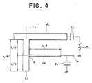
- the YIG thin film tuned oscillator of this embodiment employs an impedance matching circuit as shown in Fig. 4.
- the impedance matching circuit 3 comprises a line L1 having a quarter wavelength ⁇ /4, similar to that of the example 1, which extends at its central section perpendicularly to form a quarter wavelength line L2.
- the extended quarter wavelength line L2 has its end connected to the bias application terminal P for the drain of the GaAs FET 1, and is also grounded through a capacitor C2 by which RF components are grounded.
- a D.C. blocking capacitor C1 Provided at the end of the main line ML is a D.C. blocking capacitor C1, by which the bias is applied only to the drain of the GaAs FET 1 and it is prevented from leaking to the outside.
- the impedance matching circuit is open at the junction B of the line L2 of quarter wavelength of fundamental wave, and the line L2 does not affect the quarter wavelength line L1, resulting in the same condition as the example 1.
- the circuit is short-circuited at the junction B for the second harmonic wave, but the center of the quarter wavelength L1 is also short-circuited, and therefore the quarter wavelength line L2 does not affect the quarter wavelength L1.
- Fig. 5 shows the plot of the measured reflection coefficient ⁇ l in the case of using the impedance matching circuit 3 as shown in Fig. 4.
- ⁇ l is approximately equal to -1 for the fundamental wave of 6.5 GHz, and it is virtually equal to 0 for the second-order harmonic wave of 13 GHz.
- the example 2 is capable of suppressing the fundamental wave output and lending the second harmonic output, as in the example 1, and the second harmonic wave is used favorably as the oscillation output as in the example 1.
- the bias to the drain of the GaAs FET 1 can be given by the impedance matching circuit 3.
- the YIG thin film tuning oscillator of this embodiment employs an impedance matching circuit as shown in Fig. 6.
- the impedance matching circuit 3 comprises a main line M, which has multiple extensions of lines (short stubs) l1 - l n of quarter wavelength of second harmonic wave, with their ends being grounded.
- a D.C. blocking capacitor C1 is provided between the quarter wavelength lines l n - l and l n with the intention of biasing to the drain of the GaAs FET 1, and the quarter wavelength line l n is grounded through an RF bypass capacitor C2.
- the impedance matching circuit is open at the junction C for the second harmonic with ⁇ l being virtually 0, while it does not short-circuit for the fundamental wave and the condition of
- 1 is not met. Namely, as will be appreciated from the result of simulation shown in Fig. 7, the value of
- in the case of n 1 falls to a value as small as 0.25 at frequencies around the fundamental frequency (6.5 GHz) with respect to the second harmonic (13 GHz).
- the lines L1 and L2 of quarter wavelength of fundamental wave and the lines l1 - l n of quarter wavelength of second harmonic wave can have their width determined according to each requirement.
- the arrangement of the resonator section including the magnetic circuit is not confined to those employed in the foregoing embodiments 1, 2 and 3.
- the matching circuit is designed such that the fundamental wave generated by the ferrimagnetic resonant element and active element is reflected and the second harmonic wave is passed, whereby the load to the magnetic circuit, which applies a D.C. magnetic field necessary for frequency tuning to the ferrimagnetic resonant element, can be reduced.
Landscapes
- Inductance-Capacitance Distribution Constants And Capacitance-Resistance Oscillators (AREA)
- Waveguides (AREA)
- Oscillators With Electromechanical Resonators (AREA)
Applications Claiming Priority (2)
| Application Number | Priority Date | Filing Date | Title |
|---|---|---|---|
| JP62315650A JP2646594B2 (ja) | 1987-12-14 | 1987-12-14 | 同調発振器 |
| JP315650/87 | 1987-12-14 |
Publications (3)
| Publication Number | Publication Date |
|---|---|
| EP0320825A2 true EP0320825A2 (fr) | 1989-06-21 |
| EP0320825A3 EP0320825A3 (en) | 1989-08-23 |
| EP0320825B1 EP0320825B1 (fr) | 1995-02-15 |
Family
ID=18067921
Family Applications (1)
| Application Number | Title | Priority Date | Filing Date |
|---|---|---|---|
| EP88120660A Expired - Lifetime EP0320825B1 (fr) | 1987-12-14 | 1988-12-09 | Oscillateur accordé par grenat d'Yttrium-Fer |
Country Status (5)
| Country | Link |
|---|---|
| US (1) | US4873496A (fr) |
| EP (1) | EP0320825B1 (fr) |
| JP (1) | JP2646594B2 (fr) |
| CA (1) | CA1312658C (fr) |
| DE (1) | DE3853055D1 (fr) |
Families Citing this family (20)
| Publication number | Priority date | Publication date | Assignee | Title |
|---|---|---|---|---|
| JPH0715236A (ja) * | 1993-06-18 | 1995-01-17 | Mitsubishi Electric Corp | 周波数シンセサイザ |
| CA2190147C (fr) * | 1994-06-06 | 1999-07-06 | Adam B. Craft | Brosse a dents electrique a hautes frequences |
| US6078223A (en) * | 1998-08-14 | 2000-06-20 | The United States Of America As Represented By The Administrator Of The National Aeronautics And Space Administration | Discriminator stabilized superconductor/ferroelectric thin film local oscillator |
| US6920659B2 (en) | 2001-01-12 | 2005-07-26 | Water Pik, Inc. | Toothbrush |
| USD484311S1 (en) | 2001-01-12 | 2003-12-30 | Water Pik, Inc. | Disposable toothbrush |
| GB2394670B (en) | 2001-07-12 | 2005-01-12 | Water Pik Inc | Dual motor oral hygiene device |
| US6955539B2 (en) | 2001-07-12 | 2005-10-18 | Water Pik, Inc. | Characterization of motion of dual motor oral hygiene device |
| USD487349S1 (en) | 2002-02-01 | 2004-03-09 | Water Pik, Inc. | Dental device |
| US7198487B2 (en) | 2002-12-31 | 2007-04-03 | Water Pik, Inc. | Whitening tip for dental flossing device |
| USD500599S1 (en) | 2002-12-31 | 2005-01-11 | Water Pik, Inc. | Toothbrush handle |
| US6967540B2 (en) * | 2003-03-06 | 2005-11-22 | Paratek Microwave, Inc. | Synthesizers incorporating parascan TM varactors |
| JP4547502B2 (ja) * | 2004-09-15 | 2010-09-22 | コミサリア、ア、レネルジ、アトミク、エ、オ、エネルジ、アルテルナティブ | 強磁性薄膜同調マイクロ波発振器 |
| US8943634B2 (en) | 2011-05-02 | 2015-02-03 | Water Pik, Inc. | Mechanically-driven, sonic toothbrush system |
| KR102521242B1 (ko) | 2013-03-15 | 2023-04-17 | 워터 피크 인코포레이티드 | 기계 구동식 음파 칫솔 및 워터 플로서 |
| US9468511B2 (en) | 2013-03-15 | 2016-10-18 | Water Pik, Inc. | Electronic toothbrush with vibration dampening |
| CN205568226U (zh) | 2015-07-08 | 2016-09-14 | 洁碧有限公司 | 刷牙装置 |
| US10561480B2 (en) | 2016-05-09 | 2020-02-18 | Water Pik, Inc. | Load sensing for oral devices |
| USD844997S1 (en) | 2016-12-15 | 2019-04-09 | Water Pik, Inc. | Toothbrush handle |
| CA3128828C (fr) | 2016-12-15 | 2023-09-19 | Water Pik, Inc. | Dispositif de brossage comprenant des caracteristiques d'eclairage |
| USD845636S1 (en) | 2016-12-15 | 2019-04-16 | Water Pik, Inc. | Toothbrush handle |
Family Cites Families (7)
| Publication number | Priority date | Publication date | Assignee | Title |
|---|---|---|---|---|
| US3343069A (en) * | 1963-12-19 | 1967-09-19 | Hughes Aircraft Co | Parametric frequency doubler-limiter |
| AU470870B2 (en) * | 1973-10-29 | 1976-04-01 | Matsushita Electric Industrial Co., Ltd. | Filters employing elements with distributed constants |
| JPS6141291Y2 (fr) * | 1979-02-16 | 1986-11-25 | ||
| FR2509533B1 (fr) * | 1981-05-27 | 1986-01-03 | Labo Electronique Physique | Dispositif de polarisation d'elements actifs hyperfrequences |
| JPS58177011A (ja) * | 1982-04-10 | 1983-10-17 | Fujitsu Ltd | 発振逓倍器 |
| JPH0770918B2 (ja) * | 1984-06-05 | 1995-07-31 | ソニー株式会社 | 同調発振器 |
| JPS6157102A (ja) * | 1984-08-29 | 1986-03-24 | Fujitsu Ltd | 発振逓倍器 |
-
1987
- 1987-12-14 JP JP62315650A patent/JP2646594B2/ja not_active Expired - Fee Related
-
1988
- 1988-12-08 CA CA000585313A patent/CA1312658C/fr not_active Expired - Fee Related
- 1988-12-08 US US07/281,289 patent/US4873496A/en not_active Expired - Fee Related
- 1988-12-09 DE DE3853055T patent/DE3853055D1/de not_active Expired - Lifetime
- 1988-12-09 EP EP88120660A patent/EP0320825B1/fr not_active Expired - Lifetime
Also Published As
| Publication number | Publication date |
|---|---|
| CA1312658C (fr) | 1993-01-12 |
| JPH01157103A (ja) | 1989-06-20 |
| US4873496A (en) | 1989-10-10 |
| DE3853055D1 (de) | 1995-03-23 |
| JP2646594B2 (ja) | 1997-08-27 |
| EP0320825B1 (fr) | 1995-02-15 |
| EP0320825A3 (en) | 1989-08-23 |
Similar Documents
| Publication | Publication Date | Title |
|---|---|---|
| US4873496A (en) | Tuned oscillator | |
| EP0164684B1 (fr) | Oscillateur accordé | |
| US4264881A (en) | Microwave device provided with a 1/2 lambda resonator | |
| US5059927A (en) | Microwave oscillator with reduced phase noise | |
| CA1225126A (fr) | Diviseur de frequence par deux a microruban- microfente | |
| US4630003A (en) | FET oscillator exhibiting negative resistance due to high impedance at the source of an FET thereof | |
| US4028639A (en) | Oscillator using magnetostatic surface wave delay line | |
| Farr et al. | Novel techniques for electronic tuning of dielectric resonators | |
| US6501971B1 (en) | Magnetic ferrite microwave resonator frequency adjuster and tunable filter | |
| Tanbakuchi et al. | Magnetically tunable oscillators and filters | |
| US4945324A (en) | Thin film ferromagnetic resonance tuned filter | |
| US6114929A (en) | Magnetostatic wave device with specified distances between magnetic garnet film and ground conductors | |
| US4500858A (en) | Method for enhancing ferromagnetic coupling | |
| Marcelli et al. | A magnetostatic wave oscillator for data relay satellite | |
| Chang et al. | Magnetostatic surface wave straight-edge resonators | |
| JP2522579B2 (ja) | Pll制御を行う静磁波マイクロ波発振装置 | |
| JPH07321514A (ja) | 強磁性磁気共鳴装置 | |
| JPS6317361B2 (fr) | ||
| Marcelli et al. | A tunable, high Q magnetostatic volume wave oscillator based on straight edge YIG resonators | |
| Ishak et al. | Tunable magnetostatic wave oscillators using pure and doped YIG films | |
| JPS60242702A (ja) | マイクロ波共振回路 | |
| Lau et al. | Barium Ferrite Tuned-Indium Phosphide Gunn Millimeter Wave Oscillators | |
| JPS6120165B2 (fr) | ||
| Dupre | A 1.8 to 4.2 GHz YIG tuned transistor oscillator with a wideband buffer amplifier | |
| CA1143444A (fr) | Oscillateur accordable a mode unique utilisant les ondes magnetostatiques |
Legal Events
| Date | Code | Title | Description |
|---|---|---|---|
| PUAI | Public reference made under article 153(3) epc to a published international application that has entered the european phase |
Free format text: ORIGINAL CODE: 0009012 |
|
| AK | Designated contracting states |
Kind code of ref document: A2 Designated state(s): DE FR GB NL |
|
| PUAL | Search report despatched |
Free format text: ORIGINAL CODE: 0009013 |
|
| AK | Designated contracting states |
Kind code of ref document: A3 Designated state(s): DE FR GB NL |
|
| 17P | Request for examination filed |
Effective date: 19900222 |
|
| 17Q | First examination report despatched |
Effective date: 19920421 |
|
| GRAA | (expected) grant |
Free format text: ORIGINAL CODE: 0009210 |
|
| AK | Designated contracting states |
Kind code of ref document: B1 Designated state(s): DE FR GB NL |
|
| PG25 | Lapsed in a contracting state [announced via postgrant information from national office to epo] |
Ref country code: NL Effective date: 19950215 Ref country code: FR Effective date: 19950215 |
|
| REF | Corresponds to: |
Ref document number: 3853055 Country of ref document: DE Date of ref document: 19950323 |
|
| PG25 | Lapsed in a contracting state [announced via postgrant information from national office to epo] |
Ref country code: DE Effective date: 19950516 |
|
| EN | Fr: translation not filed | ||
| NLV1 | Nl: lapsed or annulled due to failure to fulfill the requirements of art. 29p and 29m of the patents act | ||
| PG25 | Lapsed in a contracting state [announced via postgrant information from national office to epo] |
Ref country code: GB Effective date: 19951209 |
|
| PLBE | No opposition filed within time limit |
Free format text: ORIGINAL CODE: 0009261 |
|
| STAA | Information on the status of an ep patent application or granted ep patent |
Free format text: STATUS: NO OPPOSITION FILED WITHIN TIME LIMIT |
|
| 26N | No opposition filed | ||
| GBPC | Gb: european patent ceased through non-payment of renewal fee |
Effective date: 19951209 |