EP0320971B1 - Dispositif pour la croissance épitaxiale - Google Patents
Dispositif pour la croissance épitaxiale Download PDFInfo
- Publication number
- EP0320971B1 EP0320971B1 EP88121114A EP88121114A EP0320971B1 EP 0320971 B1 EP0320971 B1 EP 0320971B1 EP 88121114 A EP88121114 A EP 88121114A EP 88121114 A EP88121114 A EP 88121114A EP 0320971 B1 EP0320971 B1 EP 0320971B1
- Authority
- EP
- European Patent Office
- Prior art keywords
- wafer
- epitaxial growth
- wafers
- radiation source
- gas
- Prior art date
- Legal status (The legal status is an assumption and is not a legal conclusion. Google has not performed a legal analysis and makes no representation as to the accuracy of the status listed.)
- Expired - Lifetime
Links
Images

Classifications
-
- C—CHEMISTRY; METALLURGY
- C30—CRYSTAL GROWTH
- C30B—SINGLE-CRYSTAL GROWTH; UNIDIRECTIONAL SOLIDIFICATION OF EUTECTIC MATERIAL OR UNIDIRECTIONAL DEMIXING OF EUTECTOID MATERIAL; REFINING BY ZONE-MELTING OF MATERIAL; PRODUCTION OF A HOMOGENEOUS POLYCRYSTALLINE MATERIAL WITH DEFINED STRUCTURE; SINGLE CRYSTALS OR HOMOGENEOUS POLYCRYSTALLINE MATERIAL WITH DEFINED STRUCTURE; AFTER-TREATMENT OF SINGLE CRYSTALS OR A HOMOGENEOUS POLYCRYSTALLINE MATERIAL WITH DEFINED STRUCTURE; APPARATUS THEREFOR
- C30B25/00—Single-crystal growth by chemical reaction of reactive gases, e.g. chemical vapour-deposition growth
- C30B25/02—Epitaxial-layer growth
- C30B25/10—Heating of the reaction chamber or the substrate
- C30B25/105—Heating of the reaction chamber or the substrate by irradiation or electric discharge
-
- C—CHEMISTRY; METALLURGY
- C30—CRYSTAL GROWTH
- C30B—SINGLE-CRYSTAL GROWTH; UNIDIRECTIONAL SOLIDIFICATION OF EUTECTIC MATERIAL OR UNIDIRECTIONAL DEMIXING OF EUTECTOID MATERIAL; REFINING BY ZONE-MELTING OF MATERIAL; PRODUCTION OF A HOMOGENEOUS POLYCRYSTALLINE MATERIAL WITH DEFINED STRUCTURE; SINGLE CRYSTALS OR HOMOGENEOUS POLYCRYSTALLINE MATERIAL WITH DEFINED STRUCTURE; AFTER-TREATMENT OF SINGLE CRYSTALS OR A HOMOGENEOUS POLYCRYSTALLINE MATERIAL WITH DEFINED STRUCTURE; APPARATUS THEREFOR
- C30B25/00—Single-crystal growth by chemical reaction of reactive gases, e.g. chemical vapour-deposition growth
- C30B25/02—Epitaxial-layer growth
-
- C—CHEMISTRY; METALLURGY
- C30—CRYSTAL GROWTH
- C30B—SINGLE-CRYSTAL GROWTH; UNIDIRECTIONAL SOLIDIFICATION OF EUTECTIC MATERIAL OR UNIDIRECTIONAL DEMIXING OF EUTECTOID MATERIAL; REFINING BY ZONE-MELTING OF MATERIAL; PRODUCTION OF A HOMOGENEOUS POLYCRYSTALLINE MATERIAL WITH DEFINED STRUCTURE; SINGLE CRYSTALS OR HOMOGENEOUS POLYCRYSTALLINE MATERIAL WITH DEFINED STRUCTURE; AFTER-TREATMENT OF SINGLE CRYSTALS OR A HOMOGENEOUS POLYCRYSTALLINE MATERIAL WITH DEFINED STRUCTURE; APPARATUS THEREFOR
- C30B29/00—Single crystals or homogeneous polycrystalline material with defined structure characterised by the material or by their shape
- C30B29/02—Elements
- C30B29/06—Silicon
Definitions
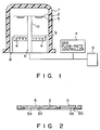
- FIG. 3 A sectional structure of a conventional vertical furnace employing RF induction heating is shown in Fig. 3.
- This vertical furnace includes quartz bell jar 31.
- Susceptor 32 is horizontally arranged in bell jar 31.
- Wafers 33 are placed on susceptor 32 such that mirror surfaces face up.
- Wafers 33 placed on susceptor 32 are heated by RF induction heating using heating coil 34.
- Gas pipe 35 is disposed at the center in bell jar 31.
- a reaction gas supplied from gas tank 38 arranged outside bell jar 31 passes through gas pipe 35 and is supplied from gas inlet 39 formed at the upper portion of gas pipe 35 to the interior to bell jar 31.
- Gas flow-rate controller 36 controls a flow rate or the like of the reaction gas supplied to bell jar 31.
- Gas outlet 37 is formed at the bottom portion of bell jar 31.
Landscapes
- Chemical & Material Sciences (AREA)
- Engineering & Computer Science (AREA)
- Crystallography & Structural Chemistry (AREA)
- Materials Engineering (AREA)
- Metallurgy (AREA)
- Organic Chemistry (AREA)
- Chemical Kinetics & Catalysis (AREA)
- General Chemical & Material Sciences (AREA)
Claims (3)
- Appareil pour la croissance épitaxiale de silicium, comprenant :- une enceinte de réaction (1) ;- des moyens de support (2), agencés à l'intérieur de ladite enceinte de réaction (1) afin de supporter au moins une plaquette semi-conductrice (5) soumise à une croissance épitaxiale ;- une source de rayonnement à infrarouge (3) agencée à l'intérieur de ladite enceinte de réaction (1) et écartée des plaquettes semi-conductrices (5) maintenues sur lesdits moyens de support (2), la source (3) étant placée à une position où des rayons infrarouges peuvent atteindre directement et chauffer les plaquettes semi-conductrices (5) ;- des moyens d'entrée de gaz (10) pour alimenter un gaz de réaction dans ladite enceinte de réaction (1) ; et- des moyens de sortie de gaz (8) pour évacuer un gaz d'échappement hors de ladite enceinte de réaction (1),
caractérisé en ce que- ladite source de rayonnement à infrarouge (3) est constituée de graphite ou d'un matériau obtenu en revêtant du graphite avec du carbure de silicium. - Appareil selon la revendication 1, caractérisé en ce que la plaquette semi-conductrice est une plaquette de silicium.
- Appareil selon la revendication 1, caractérisé en ce que lesdits moyens de support (2) supportent la plaquette semi-conductrice (5) de telle manière qu'une surface polie de celle-ci est dirigée vers le bas.
Applications Claiming Priority (2)
| Application Number | Priority Date | Filing Date | Title |
|---|---|---|---|
| JP62320427A JPH01161824A (ja) | 1987-12-18 | 1987-12-18 | 気相エピタキシャル成長装置 |
| JP320427/87 | 1987-12-18 |
Publications (3)
| Publication Number | Publication Date |
|---|---|
| EP0320971A2 EP0320971A2 (fr) | 1989-06-21 |
| EP0320971A3 EP0320971A3 (en) | 1990-09-26 |
| EP0320971B1 true EP0320971B1 (fr) | 1994-07-27 |
Family
ID=18121332
Family Applications (1)
| Application Number | Title | Priority Date | Filing Date |
|---|---|---|---|
| EP88121114A Expired - Lifetime EP0320971B1 (fr) | 1987-12-18 | 1988-12-16 | Dispositif pour la croissance épitaxiale |
Country Status (4)
| Country | Link |
|---|---|
| EP (1) | EP0320971B1 (fr) |
| JP (1) | JPH01161824A (fr) |
| KR (1) | KR930000610B1 (fr) |
| DE (1) | DE3850865T2 (fr) |
Family Cites Families (6)
| Publication number | Priority date | Publication date | Assignee | Title |
|---|---|---|---|---|
| US4499354A (en) * | 1982-10-06 | 1985-02-12 | General Instrument Corp. | Susceptor for radiant absorption heater system |
| JPS59149020A (ja) * | 1983-02-16 | 1984-08-25 | Hitachi Ltd | 縦型反応炉 |
| JPS6058613A (ja) * | 1983-09-12 | 1985-04-04 | Hitachi Ltd | エピタキシャル装置 |
| JPS60161616A (ja) * | 1984-02-01 | 1985-08-23 | Matsushita Electric Ind Co Ltd | 半導体ウエハの赤外線加熱装置 |
| JP2525348B2 (ja) * | 1984-02-09 | 1996-08-21 | 富士通株式会社 | 気相成長方法および装置 |
| EP0252667B1 (fr) * | 1986-06-30 | 1996-03-27 | Nihon Sinku Gijutsu Kabushiki Kaisha | Procédé de dépÔt en phase vapeur |
-
1987
- 1987-12-18 JP JP62320427A patent/JPH01161824A/ja active Pending
-
1988
- 1988-12-16 EP EP88121114A patent/EP0320971B1/fr not_active Expired - Lifetime
- 1988-12-16 DE DE3850865T patent/DE3850865T2/de not_active Expired - Fee Related
- 1988-12-17 KR KR1019880016875A patent/KR930000610B1/ko not_active Expired - Fee Related
Also Published As
| Publication number | Publication date |
|---|---|
| JPH01161824A (ja) | 1989-06-26 |
| EP0320971A3 (en) | 1990-09-26 |
| DE3850865D1 (de) | 1994-09-01 |
| DE3850865T2 (de) | 1994-12-08 |
| KR930000610B1 (ko) | 1993-01-25 |
| EP0320971A2 (fr) | 1989-06-21 |
| KR890011131A (ko) | 1989-08-12 |
Similar Documents
| Publication | Publication Date | Title |
|---|---|---|
| US4846102A (en) | Reaction chambers for CVD systems | |
| US5493987A (en) | Chemical vapor deposition reactor and method | |
| US3460510A (en) | Large volume semiconductor coating reactor | |
| US6113984A (en) | Gas injection system for CVD reactors | |
| EP0461194B1 (fr) | Reacteur epitaxial a capacite elevee | |
| US20030049372A1 (en) | High rate deposition at low pressures in a small batch reactor | |
| JPH0834187B2 (ja) | サセプタ | |
| EP4271852B1 (fr) | Systèmes et procédés pour une bague de préchauffage dans un réacteur de tranche de semi-conducteur | |
| EP0823491B1 (fr) | Système d'injection de gaz pour réacteurs CVD | |
| US5096534A (en) | Method for improving the reactant gas flow in a reaction chamber | |
| US5261960A (en) | Reaction chambers for CVD systems | |
| EP0164928A2 (fr) | Réacteur vertical à parois chaudes pour dépôt chimique à partir de la phase vapeur | |
| US20040178176A1 (en) | Apparatus and method for cleaning a bell jar in a barrel epitaxial reactor | |
| US6099650A (en) | Structure and method for reducing slip in semiconductor wafers | |
| JP7828348B2 (ja) | 半導体ウエハリアクタ中の輻射熱キャップのためのシステムと方法 | |
| US20010052324A1 (en) | Device for producing and processing semiconductor substrates | |
| US5913974A (en) | Heat treating method of a semiconductor single crystal substrate | |
| KR101030422B1 (ko) | 서셉터 | |
| JP3788836B2 (ja) | 気相成長用サセプタ及びその製造方法 | |
| US5044315A (en) | Apparatus for improving the reactant gas flow in a reaction chamber | |
| JP3693739B2 (ja) | 高周波誘導加熱炉 | |
| EP0320971A2 (fr) | Dispositif pour la croissance épitaxiale | |
| JP2764416B2 (ja) | サセプタ | |
| JPS6058613A (ja) | エピタキシャル装置 | |
| CN217418861U (zh) | 一种外延石墨基座 |
Legal Events
| Date | Code | Title | Description |
|---|---|---|---|
| PUAI | Public reference made under article 153(3) epc to a published international application that has entered the european phase |
Free format text: ORIGINAL CODE: 0009012 |
|
| 17P | Request for examination filed |
Effective date: 19890113 |
|
| AK | Designated contracting states |
Kind code of ref document: A2 Designated state(s): DE FR GB |
|
| PUAL | Search report despatched |
Free format text: ORIGINAL CODE: 0009013 |
|
| AK | Designated contracting states |
Kind code of ref document: A3 Designated state(s): DE FR GB |
|
| 17Q | First examination report despatched |
Effective date: 19920212 |
|
| GRAA | (expected) grant |
Free format text: ORIGINAL CODE: 0009210 |
|
| AK | Designated contracting states |
Kind code of ref document: B1 Designated state(s): DE FR GB |
|
| REF | Corresponds to: |
Ref document number: 3850865 Country of ref document: DE Date of ref document: 19940901 |
|
| ET | Fr: translation filed | ||
| PLBE | No opposition filed within time limit |
Free format text: ORIGINAL CODE: 0009261 |
|
| STAA | Information on the status of an ep patent application or granted ep patent |
Free format text: STATUS: NO OPPOSITION FILED WITHIN TIME LIMIT |
|
| 26N | No opposition filed | ||
| PGFP | Annual fee paid to national office [announced via postgrant information from national office to epo] |
Ref country code: GB Payment date: 19971208 Year of fee payment: 10 |
|
| PGFP | Annual fee paid to national office [announced via postgrant information from national office to epo] |
Ref country code: FR Payment date: 19971209 Year of fee payment: 10 |
|
| PG25 | Lapsed in a contracting state [announced via postgrant information from national office to epo] |
Ref country code: GB Free format text: LAPSE BECAUSE OF NON-PAYMENT OF DUE FEES Effective date: 19981216 |
|
| GBPC | Gb: european patent ceased through non-payment of renewal fee |
Effective date: 19981216 |
|
| PG25 | Lapsed in a contracting state [announced via postgrant information from national office to epo] |
Ref country code: FR Free format text: LAPSE BECAUSE OF NON-PAYMENT OF DUE FEES Effective date: 19990831 |
|
| REG | Reference to a national code |
Ref country code: FR Ref legal event code: ST |
|
| PGFP | Annual fee paid to national office [announced via postgrant information from national office to epo] |
Ref country code: DE Payment date: 20061214 Year of fee payment: 19 |
|
| PG25 | Lapsed in a contracting state [announced via postgrant information from national office to epo] |
Ref country code: DE Free format text: LAPSE BECAUSE OF NON-PAYMENT OF DUE FEES Effective date: 20080701 |