EP4271852B1 - Systèmes et procédés pour une bague de préchauffage dans un réacteur de tranche de semi-conducteur - Google Patents
Systèmes et procédés pour une bague de préchauffage dans un réacteur de tranche de semi-conducteur Download PDFInfo
- Publication number
- EP4271852B1 EP4271852B1 EP21844159.0A EP21844159A EP4271852B1 EP 4271852 B1 EP4271852 B1 EP 4271852B1 EP 21844159 A EP21844159 A EP 21844159A EP 4271852 B1 EP4271852 B1 EP 4271852B1
- Authority
- EP
- European Patent Office
- Prior art keywords
- edge bar
- edge
- process gas
- semiconductor wafer
- bar
- Prior art date
- Legal status (The legal status is an assumption and is not a legal conclusion. Google has not performed a legal analysis and makes no representation as to the accuracy of the status listed.)
- Active
Links
Images




Classifications
-
- C—CHEMISTRY; METALLURGY
- C23—COATING METALLIC MATERIAL; COATING MATERIAL WITH METALLIC MATERIAL; CHEMICAL SURFACE TREATMENT; DIFFUSION TREATMENT OF METALLIC MATERIAL; COATING BY VACUUM EVAPORATION, BY SPUTTERING, BY ION IMPLANTATION OR BY CHEMICAL VAPOUR DEPOSITION, IN GENERAL; INHIBITING CORROSION OF METALLIC MATERIAL OR INCRUSTATION IN GENERAL
- C23C—COATING METALLIC MATERIAL; COATING MATERIAL WITH METALLIC MATERIAL; SURFACE TREATMENT OF METALLIC MATERIAL BY DIFFUSION INTO THE SURFACE, BY CHEMICAL CONVERSION OR SUBSTITUTION; COATING BY VACUUM EVAPORATION, BY SPUTTERING, BY ION IMPLANTATION OR BY CHEMICAL VAPOUR DEPOSITION, IN GENERAL
- C23C16/00—Chemical coating by decomposition of gaseous compounds, without leaving reaction products of surface material in the coating, i.e. chemical vapour deposition [CVD] processes
- C23C16/44—Chemical coating by decomposition of gaseous compounds, without leaving reaction products of surface material in the coating, i.e. chemical vapour deposition [CVD] processes characterised by the method of coating
- C23C16/455—Chemical coating by decomposition of gaseous compounds, without leaving reaction products of surface material in the coating, i.e. chemical vapour deposition [CVD] processes characterised by the method of coating characterised by the method used for introducing gases into reaction chamber or for modifying gas flows in reaction chamber
- C23C16/45563—Gas nozzles
- C23C16/4557—Heated nozzles
-
- C—CHEMISTRY; METALLURGY
- C23—COATING METALLIC MATERIAL; COATING MATERIAL WITH METALLIC MATERIAL; CHEMICAL SURFACE TREATMENT; DIFFUSION TREATMENT OF METALLIC MATERIAL; COATING BY VACUUM EVAPORATION, BY SPUTTERING, BY ION IMPLANTATION OR BY CHEMICAL VAPOUR DEPOSITION, IN GENERAL; INHIBITING CORROSION OF METALLIC MATERIAL OR INCRUSTATION IN GENERAL
- C23C—COATING METALLIC MATERIAL; COATING MATERIAL WITH METALLIC MATERIAL; SURFACE TREATMENT OF METALLIC MATERIAL BY DIFFUSION INTO THE SURFACE, BY CHEMICAL CONVERSION OR SUBSTITUTION; COATING BY VACUUM EVAPORATION, BY SPUTTERING, BY ION IMPLANTATION OR BY CHEMICAL VAPOUR DEPOSITION, IN GENERAL
- C23C16/00—Chemical coating by decomposition of gaseous compounds, without leaving reaction products of surface material in the coating, i.e. chemical vapour deposition [CVD] processes
- C23C16/44—Chemical coating by decomposition of gaseous compounds, without leaving reaction products of surface material in the coating, i.e. chemical vapour deposition [CVD] processes characterised by the method of coating
- C23C16/455—Chemical coating by decomposition of gaseous compounds, without leaving reaction products of surface material in the coating, i.e. chemical vapour deposition [CVD] processes characterised by the method of coating characterised by the method used for introducing gases into reaction chamber or for modifying gas flows in reaction chamber
- C23C16/45502—Flow conditions in reaction chamber
- C23C16/45504—Laminar flow
-
- C—CHEMISTRY; METALLURGY
- C23—COATING METALLIC MATERIAL; COATING MATERIAL WITH METALLIC MATERIAL; CHEMICAL SURFACE TREATMENT; DIFFUSION TREATMENT OF METALLIC MATERIAL; COATING BY VACUUM EVAPORATION, BY SPUTTERING, BY ION IMPLANTATION OR BY CHEMICAL VAPOUR DEPOSITION, IN GENERAL; INHIBITING CORROSION OF METALLIC MATERIAL OR INCRUSTATION IN GENERAL
- C23C—COATING METALLIC MATERIAL; COATING MATERIAL WITH METALLIC MATERIAL; SURFACE TREATMENT OF METALLIC MATERIAL BY DIFFUSION INTO THE SURFACE, BY CHEMICAL CONVERSION OR SUBSTITUTION; COATING BY VACUUM EVAPORATION, BY SPUTTERING, BY ION IMPLANTATION OR BY CHEMICAL VAPOUR DEPOSITION, IN GENERAL
- C23C16/00—Chemical coating by decomposition of gaseous compounds, without leaving reaction products of surface material in the coating, i.e. chemical vapour deposition [CVD] processes
- C23C16/44—Chemical coating by decomposition of gaseous compounds, without leaving reaction products of surface material in the coating, i.e. chemical vapour deposition [CVD] processes characterised by the method of coating
- C23C16/455—Chemical coating by decomposition of gaseous compounds, without leaving reaction products of surface material in the coating, i.e. chemical vapour deposition [CVD] processes characterised by the method of coating characterised by the method used for introducing gases into reaction chamber or for modifying gas flows in reaction chamber
- C23C16/45582—Expansion of gas before it reaches the substrate
-
- C—CHEMISTRY; METALLURGY
- C23—COATING METALLIC MATERIAL; COATING MATERIAL WITH METALLIC MATERIAL; CHEMICAL SURFACE TREATMENT; DIFFUSION TREATMENT OF METALLIC MATERIAL; COATING BY VACUUM EVAPORATION, BY SPUTTERING, BY ION IMPLANTATION OR BY CHEMICAL VAPOUR DEPOSITION, IN GENERAL; INHIBITING CORROSION OF METALLIC MATERIAL OR INCRUSTATION IN GENERAL
- C23C—COATING METALLIC MATERIAL; COATING MATERIAL WITH METALLIC MATERIAL; SURFACE TREATMENT OF METALLIC MATERIAL BY DIFFUSION INTO THE SURFACE, BY CHEMICAL CONVERSION OR SUBSTITUTION; COATING BY VACUUM EVAPORATION, BY SPUTTERING, BY ION IMPLANTATION OR BY CHEMICAL VAPOUR DEPOSITION, IN GENERAL
- C23C16/00—Chemical coating by decomposition of gaseous compounds, without leaving reaction products of surface material in the coating, i.e. chemical vapour deposition [CVD] processes
- C23C16/44—Chemical coating by decomposition of gaseous compounds, without leaving reaction products of surface material in the coating, i.e. chemical vapour deposition [CVD] processes characterised by the method of coating
- C23C16/455—Chemical coating by decomposition of gaseous compounds, without leaving reaction products of surface material in the coating, i.e. chemical vapour deposition [CVD] processes characterised by the method of coating characterised by the method used for introducing gases into reaction chamber or for modifying gas flows in reaction chamber
- C23C16/45587—Mechanical means for changing the gas flow
- C23C16/45591—Fixed means, e.g. wings, baffles
-
- C—CHEMISTRY; METALLURGY
- C23—COATING METALLIC MATERIAL; COATING MATERIAL WITH METALLIC MATERIAL; CHEMICAL SURFACE TREATMENT; DIFFUSION TREATMENT OF METALLIC MATERIAL; COATING BY VACUUM EVAPORATION, BY SPUTTERING, BY ION IMPLANTATION OR BY CHEMICAL VAPOUR DEPOSITION, IN GENERAL; INHIBITING CORROSION OF METALLIC MATERIAL OR INCRUSTATION IN GENERAL
- C23C—COATING METALLIC MATERIAL; COATING MATERIAL WITH METALLIC MATERIAL; SURFACE TREATMENT OF METALLIC MATERIAL BY DIFFUSION INTO THE SURFACE, BY CHEMICAL CONVERSION OR SUBSTITUTION; COATING BY VACUUM EVAPORATION, BY SPUTTERING, BY ION IMPLANTATION OR BY CHEMICAL VAPOUR DEPOSITION, IN GENERAL
- C23C16/00—Chemical coating by decomposition of gaseous compounds, without leaving reaction products of surface material in the coating, i.e. chemical vapour deposition [CVD] processes
- C23C16/44—Chemical coating by decomposition of gaseous compounds, without leaving reaction products of surface material in the coating, i.e. chemical vapour deposition [CVD] processes characterised by the method of coating
- C23C16/458—Chemical coating by decomposition of gaseous compounds, without leaving reaction products of surface material in the coating, i.e. chemical vapour deposition [CVD] processes characterised by the method of coating characterised by the method used for supporting substrates in the reaction chamber
- C23C16/4582—Rigid and flat substrates, e.g. plates or discs
- C23C16/4583—Rigid and flat substrates, e.g. plates or discs the substrate being supported substantially horizontally
- C23C16/4585—Devices at or outside the perimeter of the substrate support, e.g. clamping rings, shrouds
-
- C—CHEMISTRY; METALLURGY
- C30—CRYSTAL GROWTH
- C30B—SINGLE-CRYSTAL GROWTH; UNIDIRECTIONAL SOLIDIFICATION OF EUTECTIC MATERIAL OR UNIDIRECTIONAL DEMIXING OF EUTECTOID MATERIAL; REFINING BY ZONE-MELTING OF MATERIAL; PRODUCTION OF A HOMOGENEOUS POLYCRYSTALLINE MATERIAL WITH DEFINED STRUCTURE; SINGLE CRYSTALS OR HOMOGENEOUS POLYCRYSTALLINE MATERIAL WITH DEFINED STRUCTURE; AFTER-TREATMENT OF SINGLE CRYSTALS OR A HOMOGENEOUS POLYCRYSTALLINE MATERIAL WITH DEFINED STRUCTURE; APPARATUS THEREFOR
- C30B25/00—Single-crystal growth by chemical reaction of reactive gases, e.g. chemical vapour-deposition growth
- C30B25/02—Epitaxial-layer growth
- C30B25/12—Substrate holders or susceptors
-
- C—CHEMISTRY; METALLURGY
- C30—CRYSTAL GROWTH
- C30B—SINGLE-CRYSTAL GROWTH; UNIDIRECTIONAL SOLIDIFICATION OF EUTECTIC MATERIAL OR UNIDIRECTIONAL DEMIXING OF EUTECTOID MATERIAL; REFINING BY ZONE-MELTING OF MATERIAL; PRODUCTION OF A HOMOGENEOUS POLYCRYSTALLINE MATERIAL WITH DEFINED STRUCTURE; SINGLE CRYSTALS OR HOMOGENEOUS POLYCRYSTALLINE MATERIAL WITH DEFINED STRUCTURE; AFTER-TREATMENT OF SINGLE CRYSTALS OR A HOMOGENEOUS POLYCRYSTALLINE MATERIAL WITH DEFINED STRUCTURE; APPARATUS THEREFOR
- C30B25/00—Single-crystal growth by chemical reaction of reactive gases, e.g. chemical vapour-deposition growth
- C30B25/02—Epitaxial-layer growth
- C30B25/14—Feed and outlet means for the gases; Modifying the flow of the reactive gases
-
- C—CHEMISTRY; METALLURGY
- C30—CRYSTAL GROWTH
- C30B—SINGLE-CRYSTAL GROWTH; UNIDIRECTIONAL SOLIDIFICATION OF EUTECTIC MATERIAL OR UNIDIRECTIONAL DEMIXING OF EUTECTOID MATERIAL; REFINING BY ZONE-MELTING OF MATERIAL; PRODUCTION OF A HOMOGENEOUS POLYCRYSTALLINE MATERIAL WITH DEFINED STRUCTURE; SINGLE CRYSTALS OR HOMOGENEOUS POLYCRYSTALLINE MATERIAL WITH DEFINED STRUCTURE; AFTER-TREATMENT OF SINGLE CRYSTALS OR A HOMOGENEOUS POLYCRYSTALLINE MATERIAL WITH DEFINED STRUCTURE; APPARATUS THEREFOR
- C30B29/00—Single crystals or homogeneous polycrystalline material with defined structure characterised by the material or by their shape
- C30B29/02—Elements
- C30B29/06—Silicon
-
- H—ELECTRICITY
- H10—SEMICONDUCTOR DEVICES; ELECTRIC SOLID-STATE DEVICES NOT OTHERWISE PROVIDED FOR
- H10P—GENERIC PROCESSES OR APPARATUS FOR THE MANUFACTURE OR TREATMENT OF DEVICES COVERED BY CLASS H10
- H10P14/00—Formation of materials, e.g. in the shape of layers or pillars
- H10P14/20—Formation of materials, e.g. in the shape of layers or pillars of semiconductor materials
- H10P14/24—Formation of materials, e.g. in the shape of layers or pillars of semiconductor materials using chemical vapour deposition [CVD]
-
- H—ELECTRICITY
- H10—SEMICONDUCTOR DEVICES; ELECTRIC SOLID-STATE DEVICES NOT OTHERWISE PROVIDED FOR
- H10P—GENERIC PROCESSES OR APPARATUS FOR THE MANUFACTURE OR TREATMENT OF DEVICES COVERED BY CLASS H10
- H10P14/00—Formation of materials, e.g. in the shape of layers or pillars
- H10P14/20—Formation of materials, e.g. in the shape of layers or pillars of semiconductor materials
- H10P14/29—Formation of materials, e.g. in the shape of layers or pillars of semiconductor materials characterised by the substrates
- H10P14/2901—Materials
- H10P14/2902—Materials being Group IVA materials
- H10P14/2905—Silicon, silicon germanium or germanium
-
- H—ELECTRICITY
- H10—SEMICONDUCTOR DEVICES; ELECTRIC SOLID-STATE DEVICES NOT OTHERWISE PROVIDED FOR
- H10P—GENERIC PROCESSES OR APPARATUS FOR THE MANUFACTURE OR TREATMENT OF DEVICES COVERED BY CLASS H10
- H10P14/00—Formation of materials, e.g. in the shape of layers or pillars
- H10P14/20—Formation of materials, e.g. in the shape of layers or pillars of semiconductor materials
- H10P14/34—Deposited materials, e.g. layers
- H10P14/3402—Deposited materials, e.g. layers characterised by the chemical composition
- H10P14/3404—Deposited materials, e.g. layers characterised by the chemical composition being Group IVA materials
- H10P14/3411—Silicon, silicon germanium or germanium
-
- C—CHEMISTRY; METALLURGY
- C23—COATING METALLIC MATERIAL; COATING MATERIAL WITH METALLIC MATERIAL; CHEMICAL SURFACE TREATMENT; DIFFUSION TREATMENT OF METALLIC MATERIAL; COATING BY VACUUM EVAPORATION, BY SPUTTERING, BY ION IMPLANTATION OR BY CHEMICAL VAPOUR DEPOSITION, IN GENERAL; INHIBITING CORROSION OF METALLIC MATERIAL OR INCRUSTATION IN GENERAL
- C23C—COATING METALLIC MATERIAL; COATING MATERIAL WITH METALLIC MATERIAL; SURFACE TREATMENT OF METALLIC MATERIAL BY DIFFUSION INTO THE SURFACE, BY CHEMICAL CONVERSION OR SUBSTITUTION; COATING BY VACUUM EVAPORATION, BY SPUTTERING, BY ION IMPLANTATION OR BY CHEMICAL VAPOUR DEPOSITION, IN GENERAL
- C23C16/00—Chemical coating by decomposition of gaseous compounds, without leaving reaction products of surface material in the coating, i.e. chemical vapour deposition [CVD] processes
- C23C16/44—Chemical coating by decomposition of gaseous compounds, without leaving reaction products of surface material in the coating, i.e. chemical vapour deposition [CVD] processes characterised by the method of coating
- C23C16/455—Chemical coating by decomposition of gaseous compounds, without leaving reaction products of surface material in the coating, i.e. chemical vapour deposition [CVD] processes characterised by the method of coating characterised by the method used for introducing gases into reaction chamber or for modifying gas flows in reaction chamber
- C23C16/45563—Gas nozzles
-
- C—CHEMISTRY; METALLURGY
- C23—COATING METALLIC MATERIAL; COATING MATERIAL WITH METALLIC MATERIAL; CHEMICAL SURFACE TREATMENT; DIFFUSION TREATMENT OF METALLIC MATERIAL; COATING BY VACUUM EVAPORATION, BY SPUTTERING, BY ION IMPLANTATION OR BY CHEMICAL VAPOUR DEPOSITION, IN GENERAL; INHIBITING CORROSION OF METALLIC MATERIAL OR INCRUSTATION IN GENERAL
- C23C—COATING METALLIC MATERIAL; COATING MATERIAL WITH METALLIC MATERIAL; SURFACE TREATMENT OF METALLIC MATERIAL BY DIFFUSION INTO THE SURFACE, BY CHEMICAL CONVERSION OR SUBSTITUTION; COATING BY VACUUM EVAPORATION, BY SPUTTERING, BY ION IMPLANTATION OR BY CHEMICAL VAPOUR DEPOSITION, IN GENERAL
- C23C16/00—Chemical coating by decomposition of gaseous compounds, without leaving reaction products of surface material in the coating, i.e. chemical vapour deposition [CVD] processes
- C23C16/44—Chemical coating by decomposition of gaseous compounds, without leaving reaction products of surface material in the coating, i.e. chemical vapour deposition [CVD] processes characterised by the method of coating
- C23C16/458—Chemical coating by decomposition of gaseous compounds, without leaving reaction products of surface material in the coating, i.e. chemical vapour deposition [CVD] processes characterised by the method of coating characterised by the method used for supporting substrates in the reaction chamber
- C23C16/4582—Rigid and flat substrates, e.g. plates or discs
- C23C16/4587—Rigid and flat substrates, e.g. plates or discs the substrate being supported substantially vertically
- C23C16/4588—Rigid and flat substrates, e.g. plates or discs the substrate being supported substantially vertically the substrate being rotated
-
- C—CHEMISTRY; METALLURGY
- C30—CRYSTAL GROWTH
- C30B—SINGLE-CRYSTAL GROWTH; UNIDIRECTIONAL SOLIDIFICATION OF EUTECTIC MATERIAL OR UNIDIRECTIONAL DEMIXING OF EUTECTOID MATERIAL; REFINING BY ZONE-MELTING OF MATERIAL; PRODUCTION OF A HOMOGENEOUS POLYCRYSTALLINE MATERIAL WITH DEFINED STRUCTURE; SINGLE CRYSTALS OR HOMOGENEOUS POLYCRYSTALLINE MATERIAL WITH DEFINED STRUCTURE; AFTER-TREATMENT OF SINGLE CRYSTALS OR A HOMOGENEOUS POLYCRYSTALLINE MATERIAL WITH DEFINED STRUCTURE; APPARATUS THEREFOR
- C30B25/00—Single-crystal growth by chemical reaction of reactive gases, e.g. chemical vapour-deposition growth
- C30B25/02—Epitaxial-layer growth
- C30B25/10—Heating of the reaction chamber or the substrate
Definitions
- the field relates generally to apparatus and methods for wafer processing, and more particularly to apparatus and methods for semiconductor wafer chemical vapor deposition processes.
- Epitaxial chemical vapor deposition is a process for growing a thin layer of material on a semiconductor wafer so that the lattice structure is identical to that of the wafer.
- Epitaxial CVD is widely used in semiconductor wafer production to build up epitaxial layers such that devices can be fabricated directly on the epitaxial layer.
- the epitaxial deposition process begins by introducing a cleaning gas, such as hydrogen or a hydrogen and hydrogen chloride mixture, to a front surface of the wafer (i.e., a surface facing away from the susceptor) to pre-heat and clean the front surface of the wafer.
- the cleaning gas removes native oxide from the front surface, permitting the epitaxial silicon layer to grow continuously and evenly on the surface during a subsequent step of the deposition process.
- the epitaxial deposition process continues by introducing a vaporous silicon source gas, such as silane or a chlorinated silane, to the front surface of the wafer to deposit and grow an epitaxial layer of silicon on the front surface.
- a vaporous silicon source gas such as silane or a chlorinated silane
- a back surface opposite the front surface of the susceptor may be simultaneously subjected to hydrogen gas.
- the susceptor which supports the semiconductor wafer in the deposition chamber during the epitaxial deposition, is rotated during the process to allow the epitaxial layer to grow evenly.
- epitaxial CVD growth rates are generally not uniform across the surface of each wafer because of non-uniform flow rates within the reactor.
- a lack of uniformity causes degradation in the flatness of the wafer and may be a result of variability or local flowrate deviations within the deposition chamber during the epitaxial deposition. Accordingly, there exists a need for a practical, cost-effective apparatus to improve local flowrate deviations to improve uniformity of epitaxial CVD growth rates.
- US 2015/020734 A1 discloses a CVD apparatus for epitaxial layer growth with a preheat ring for process gas preheating.
- the process gas horizontally flows over the wafer and at the side of the process gas inlet, the surface of the preheat ring is profiled and includes fins or protrusions.
- a reaction apparatus for contacting a process gas with a semiconductor wafer.
- the reaction apparatus includes an upper dome, a lower dome, an upper liner, a lower liner, and a preheat ring.
- the lower dome attached to the upper dome.
- the upper dome and the lower dome define a reaction chamber.
- the lower liner is positioned below the upper liner.
- the upper liner and the lower liner define a process gas inlet for channeling the process gas into the reaction chamber.
- the preheat ring is positioned within the reaction chamber for heating the process gas prior to contacting the semiconductor wafer.
- the preheating ring is attached to an inner circumference of the lower liner.
- the preheat ring includes an annular disk and an edge bar.
- the annular disk has an inner edge, an outer edge, a first side, and a second side opposite the first side.
- the inner edge and the outer edge define a radial distance therebetween.
- the edge bar positioned on the first side and extending from the outer edge toward the inner edge an edge bar radial thickness. The radial distance is greater than the edge bar radial thickness.
- a preheat ring positioned within a reaction apparatus for heating a process gas prior to contacting a semiconductor wafer during a wafering process.
- the preheat ring includes an annular disk and an edge bar.
- the annular disk has an inner edge, an outer edge, a first side, and a second side opposite the first side.
- the inner edge and the outer edge define a radial distance therebetween.
- the edge bar is positioned on the first side and extends from the outer edge toward the inner edge an edge bar radial thickness. The radial distance is greater than the edge bar radial thickness.
- a method of manufacturing a semiconductor wafer in a reaction apparatus includes an upper dome and a lower dome defining a reaction chamber and an upper liner and a lower liner defining a process gas inlet.
- the reaction apparatus further includes a preheat ring positioned within the reaction chamber for heating the process gas prior to contacting the semiconductor wafer.
- the preheating ring is attached to an inner circumference of the lower liner and includes an annular disk and an edge bar positioned on the annular disk.
- the method includes channeling a process gas into the reaction chamber through the process gas inlet.
- the method also includes heating the process gas with the preheat ring.
- the method further includes adjusting at least one of a velocity and a direction of the process gas with the edge bar.
- the method also includes depositing a layer on the semiconductor wafer with the process gas.
- the edge bar facilitates forming a uniform thickness of the layer on the semiconductor wafer.
- an apparatus for depositing an epitaxial layer on a semiconductor substrate in accordance with an embodiment of the present disclosure is generally referred to as 100.
- the illustrated apparatus is a single wafer reactor (i.e., a 300mm AMAT Centura reactor); however, the apparatus and methods disclosed herein for providing a more uniform epitaxial layer are suitable for use in other reactor designs including, for example, multiple wafer reactors.
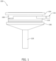
- the apparatus 100 includes a reaction chamber 102 comprising an upper dome 104, a lower dome 106, an upper liner 108, and a lower liner 110.
- the upper dome 104, lower dome 106, upper liner 108, and lower liner 110 define an interior space 112 of the reaction chamber 102 in which process gas contacts a semiconductor wafer 114.
- a gas manifold 116 is used to direct process gas into the reaction chamber 102.
- a perspective view of the reaction chamber 102 and gas manifold 116 is shown in Figure 2 .
- the apparatus 100 is a 300mm AMAT Centura reactor. In alternative embodiments, the apparatus 100 may be any type of reactor.
- the apparatus 100 may be used to process a wafer in a wafering process, including without limitation, depositing any type of material on a wafer performed by a chemical vapor deposition (CVD) process, such as epitaxial CVD or polycrystalline CVD.
- CVD chemical vapor deposition
- epitaxy and/or CVD processes should not be considered limiting as the apparatus 100 may also be used for other purposes such as to perform etching or smoothing processes on the wafer.
- the wafer shown herein is generally circular in shape, though wafers of other shapes are contemplated within the scope of this disclosure.
- the apparatus 100 is shown in cross section to better illustrate the apparatus in Figure 3 .
- a preheat ring 118 for heating the process gas prior to contact with a semiconductor wafer 114.
- the outside circumference of the preheat ring 118 is attached to the inner circumference of the lower liner 110.
- the preheat ring 118 may be supported by an annular ledge 170 of the lower liner 110.
- a susceptor 120 (which may also be referred to herein as a "susceptor body”) traversing the space interior to the preheat ring 118 supports the semiconductor wafer 114.
- Process gas may be heated prior to contacting the semiconductor wafer 114.
- Both the preheat ring 118 and the susceptor 120 are generally opaque to absorb radiant heating light produced by high intensity lamps 122, 124 that may be located above and below the reaction chamber 102. Maintaining the preheat ring 118 and the susceptor 120 at a temperature above ambient allows the preheat ring 118 and the susceptor 120 to transfer heat to the process gas as the process gas passes over the preheat ring and the susceptor.
- the diameter of the semiconductor wafer 114 is less than the diameter of the susceptor 120 to allow the susceptor to heat the process gas before it contacts the wafer.
- the preheat ring 118 and susceptor 120 may suitably be constructed of opaque graphite coated with silicon carbide, though other materials are contemplated.
- the upper dome 104 and lower dome 106 are typically made of a transparent material to allow radiant heating light to pass into the reaction chamber 102 and onto the preheat ring 118 and the susceptor 120.
- the upper dome 104 and lower dome 106 may be constructed of transparent quartz. Quartz is generally transparent to infrared and visible light and is chemically stable under the reaction conditions of the deposition reaction.
- Equipment other than high intensity lamps 122, 124 may be used to provide heat to the reaction chamber such as, for example, resistance heaters and inductive heaters.
- An infrared temperature sensor such as a pyrometer may be mounted on the reaction chamber 102 to monitor the temperature of the susceptor 120, preheat ring 118, or semiconductor wafer 114 by receiving infrared radiation emitted by the susceptor, preheat ring, or wafer.
- the apparatus 100 includes a shaft 126 that may support the susceptor 120.
- the shaft 126 extends through a central column 128.
- the shaft 126 includes a first end 130 attached to the central column 128 and a second end 132 positioned proximate a center region 134 of the semiconductor wafer 114.
- the shaft 126 has a shaft diameter 136 of about 5 millimeters (mm) to about 10 mm.
- the shaft 126 is connected to a suitable rotation mechanism (not shown) for rotation of the shaft 126, susceptor 120, and semiconductor wafer 114 about a longitudinal axis X with respect to the apparatus 100.
- the outside edge of the susceptor 120 and inside edge of the preheat ring 118 ( Fig. 3 ) are separated by a gap 138 to allow rotation of the susceptor.
- the semiconductor wafer 114 is rotated to prevent an excess of material from being deposited on the wafer leading edge and provide a more uniform epitaxial layer.
- the preheat ring 118 modifies or tunes the process gas prior to contact with the semiconductor wafer 114 in order to improve the growth rate on the semiconductor wafer and create a more uniform radial deposition profile.
- the upper liner 108 and the lower liner 110 define a process gas inlet 140 and a process gas outlet 142.
- the process gas inlet 140 channels process gas into the reaction chamber 102, and the process gas outlet 142 channels process gas out of the reaction chamber.
- the process gas is channeled from the process gas inlet 140 to the process gas outlet 142 within the reaction chamber 102 as the semiconductor wafer 114 is rotated within the reaction chamber.
- the process gas inlet 140 may be separated into inlet segments 186, 188, 190, 192 each having a segment height 194 and a segment width 196.
- Each inlet segment 186, 188, 190, 192 channels process gas to a different portion of the semiconductor wafer 114. For example, as illustrated in FIG.
- the upper liner 108 and the lower liner 110 define a first inlet segment 186 that channels process gas to an edge 144 of the semiconductor wafer 114, a second inlet segment 188 that channels process gas the center region 134 of the semiconductor wafer 114, a third inlet segment 190 that also channels process gas the center region 134 of the semiconductor wafer 114, and a fourth inlet segment 192 that also channels process gas to the edge 144 of the semiconductor wafer 114.
- the growth rate of the semiconductor wafer 114 at an edge 144 of the semiconductor wafer is greater than the growth rate of the center region 134 of the semiconductor wafer. Increased growth rate at the edge 144 relative to the center region 134 may generate a non-uniform radial deposition profile and a non-uniform thickness of the semiconductor wafer 114.
- the preheat ring 118 described herein modifies or tunes the process gas prior to contact with the semiconductor wafer 114 in order to improve the growth rate on the semiconductor wafer, create a more uniform radial deposition profile, and manufacture semiconductor wafers with a uniform thickness.
- the preheat ring 118 includes an annular disk 146 and an edge bar 148 attached to the annular disk.
- the annular disk 146 defines an inner edge 150 defining a disk hole 152 and an inner diameter 154, an outer edge 156 defining an outer diameter 158, a first side 160, a second side 162, and a disk thickness 164 between the first and second side.
- the inner diameter 154 is greater than a susceptor diameter 166 of the susceptor 120 such that the preheat ring 118 circumscribes the susceptor.
- the preheat ring 118 shown herein is generally circular in shape to compliment the shape of the semiconductor wafer 114, though preheat rings of other shapes are contemplated within the scope of this disclosure to compliment wafers of other shapes.
- the outer diameter 158 is smaller than a liner diameter 168 of the lower liner 110 such that the lower liner circumscribes the preheat ring 118 and the semiconductor wafer 114.
- the annular disk 146 extends from the inner edge 150 to the outer edge 156 a radial distance 172.
- the radial distance 172 is configured to enable the preheat ring 118 to absorb heat from the high intensity lamps 122 and 124 and transfer the absorbed heat to the process gas as the process gas passes over the preheat ring.
- the edge bar 148 extends from the first side 160 of the annular disk 146 and modifies or tunes the process gas prior to contact with the semiconductor wafer 114 in order to improve the growth rate on the semiconductor wafer and create a more uniform radial deposition profile. Specifically, the edge bar 148 modifies, tunes, and/or changes at least one of a direction of flow of the process gas, a velocity of the process gas, and a flow rate of the process gas in order to improve the growth rate on the semiconductor wafer and create a more uniform radial deposition profile.
- the preheat ring 118 includes two edge bars 148. In alternative embodiments, the preheat ring 118 includes one edge bar 148. In yet another alternative embodiment, the preheat ring 118 may include multiple smaller edge bars 148. Accordingly, the preheat ring 118 may include at least one edge bar 148 and/or a plurality of edge bars 148 depending on the flow of process gas within the reaction chamber 102. More specifically, simulations and/or experimental results may be used to determine the number and position of edge bars 148 on the preheat ring 118 in order to improve the growth rate on the semiconductor wafer 114 and create a more uniform radial deposition profile.
- the edge bars 148 is suitably made of opaque graphite coated with silicon carbide, though other materials are contemplated. In other embodiments, rather than being opaque, the edge bar 148 may be made of a translucent or transparent material.
- the edge bar 148 is suitably positioned proximate the outer edge 156 of the annular disk 146, proximate the process gas inlet 140, and proximate specific regions of the semiconductor wafer 114 to correct and/or affect the growth rate of the semiconductor wafer 114 during processing, such as epitaxial deposition to alleviate non-uniformities.
- the edge bar 148 is positioned proximate the process gas inlet 140 to cause the velocity or flow rate of the process gas at the edge 144 of the semiconductor wafer 114 to increase (relative to when an edge bar is not used) thereby decreasing the amount of material (e.g., silicon) that deposits at the edge of the semiconductor wafer during epitaxial CVD processes.
- the position of the edge bar 148 proximate the process gas inlet may cause the direction of the process gas at the edge 144 of the semiconductor wafer 114 to change (relative to when an edge bar is not used) thereby decreasing the amount of material (e.g., silicon) that deposits in the edge of the semiconductor wafer during epitaxial CVD processes.
- the edge bar 148 is suitably positioned proximate the outer edge 156 of the annular disk 146 proximate the process gas inlet 140 to modify the process gas as it enters the reaction chamber 102.
- the edge bar 148 may be positioned at any location on the preheat ring 118 that enables the edge bar 148 to operate as described herein.
- the edge bar 148 is positioned relative to the semiconductor wafer 114 to correct and/or affect the growth rate of non-uniformities of the semiconductor wafer 114 during processing.
- a simulation and/or experimentation may be used to determine where non-uniformities occur on the semiconductor wafer 114 when an edge bar is not used, and the edge bar 148 may be positioned on the preheat ring 118 to alleviate the non-uniformities.
- the edge bar 148 may be positioned proximate the edge 144 of the semiconductor wafer 114 to cause the velocity or flow rate of the process gas at the edge to increase (relative to when an edge bar is not used) thereby decreasing the amount of material (e.g., silicon) that deposits at the edge of the semiconductor wafer during epitaxial CVD processes. Additionally, the edge bar 148 may be positioned proximate the edge 144 of the semiconductor wafer 114 to cause the direction of the process gas at the edge to change (relative to when an edge bar is not used) thereby decreasing the amount of material (e.g., silicon) that deposits in the edge of the semiconductor wafer during epitaxial CVD processes.
- material e.g., silicon
- the edge bars 148 of the illustrated embodiment are positioned immediately downstream of the first inlet segment 186 and the fourth inlet segment 192 to increase the velocity, increase the flow rate, and/or change the direction of the process gas directed toward the edge 144 of the semiconductor wafer 114.
- the edge bar 148 is suitably positioned proximate the edge 144 of the semiconductor wafer 114 in which a localized or global maximum layer thickness occurs to decrease the deposition at the edge and create a more uniform radial deposition profile. Note that this maximum layer thickness may be a local or global maximum, and may generally be referred to as a non-uniformity.
- the thickness profile may be determined by use of any suitable method available to those of skill in the art including, for example, use of a Fourier-Transform Infrared (FTIR) spectrometer or use of a wafer flatness tool (e.g., KLA-Tencor Wafersight or WaferSight2; Milpitas, California).
- FTIR Fourier-Transform Infrared
- wafer flatness tool e.g., KLA-Tencor Wafersight or WaferSight2; Milpitas, California.
- the radial thickness profile of the substrate is determined before material deposition (e.g., before deposition of an epitaxial layer) and the thickness profile of the layered structure may then be measured.
- the thickness profile of the deposited layer may be determined by subtracting the substrate thickness from the layered structure thickness.
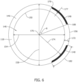
- each edge bar 148 is positioned on the preheat ring 118 such that each edge bar defines an edge bar radius 174, an edge bar angle ⁇ relative to a center 176 of the semiconductor wafer 114, and an edge bar radial thickness 177.
- the edge bar 148 has a first end 178 and a second end 180, and the edge bar angle ⁇ is the angle defined between the center 176 of the semiconductor wafer 114, the first end, and the second end.
- the edge bar 148 also defines an edge bar circumferential length 182 between the first end 178 and the second end 180 and has an edge bar height 184 and an edge bar radial width 187. Additionally, the radial distance 172 is greater than the edge bar radial thickness 177.
- the edge bar 148 is a bump or rounded protrusion extending from the first side 160 of the preheat ring 118.
- the edge bar 148 may have any shape that enables the edge bar to operate as described herein.
- the edge bar 148 is curved such that the edge bar forms an arc segment complimentary to the shape of the outer edge 156 of the preheat ring 118.
- the edge bar 148 may have any shape that enables the edge bar to operate as described herein.
- the edge bar 148 may be shaped to include various projections and/or notches or recesses. The edge bar 148 may also be beveled or rounded.
- Such non-uniform shapes may enable the edge bar 148 to correct and/or affect the growth rate of non-uniformities of the semiconductor wafer 114 during processing. For example, analysis of the thickness profile of the semiconductor wafer 114 may identify regions outside of the edges 144 that have decreased velocity or flow rate such that the deposition of material in those areas is non-uniform. The shape of the edge bar 148 may be adjusted to correct and/or affect the flow of process gas to those regions to decrease material deposition within those regions.
- the inner diameter 154 is about 240 mm to about 252 mm; the outer diameter 158 is about 296 mm to about 308 mm; the disk thickness 164 is about 4 mm to about 10 mm; the susceptor diameter 166 is about 240 mm to about 252 mm; the liner diameter 168 is about 296 mm to about 308 mm; the radial distance 172 is about 44 mm to about 68 mm; the edge bar radius 174 is about 143 mm to about 149 mm; the edge bar circumferential length 182 is about 20 mm to about 60 mm; the edge bar height 184 is about 0.5 mm to about 2 mm; the edge bar angle ⁇ is about 20° to about 50°; the segment height 194 is about 5 mm to about 8 mm; and the segment width 196 is about 238 mm to about 248 mm.
- the inner diameter 154, the outer diameter 158, the disk thickness 164, the susceptor diameter 166, the liner diameter 168, the radial distance 172, the edge bar radius 174, the edge bar circumferential length 182, the edge bar height 184, the edge bar angle ⁇ , the segment height 194, and the segment width 196 may be any distance or angle that enables the edge bar 148 to operate as described herein.
- the inner diameter 154, the outer diameter 158, the disk thickness 164, the susceptor diameter 166, the liner diameter 168, the radial distance 172, the edge bar radius 174, the edge bar circumferential length 182, the edge bar height 184, the edge bar angle ⁇ , the segment height 194, and the segment width 196 are suitably chosen depending on a location and size of a local or global epitaxial layer thickness minimum or maximum.
- the edge bar height 184 is configured to increase the velocity, increase the flow rate, and/or change the direction of the process gas directed toward the edge 144 of the semiconductor wafer 114.
- the edge bar height 184 is about 0.5 % to about 50 % of the segment height 194. Increasing the edge bar height 184 relative to the segment height 194 generally results increased process gas velocity, flow rate, and/or a change in direction of the process gas which results in deposition of less material on the semiconductor wafer 114 in portions of the semiconductor wafer proximate the edge bar 148.
- edge bar height 184 decreases the edge bar height 184 relative to the segment height 194 generally results decreased process gas velocity, flow rate, and/or less change in direction of the process gas which results in deposition of more material on the semiconductor wafer 114 in portions of the semiconductor wafer proximate the edge bar 148. Therefore, the amount of material deposited on portions of the semiconductor wafer 114 proximate the edge bar 148 is adjusted by varying the edge bar height 184.
- the edge bar circumferential length 182 is also configured to increase the velocity, increase the flow rate, and/or change the direction of the process gas directed toward the edge 144 of the semiconductor wafer 114.
- the edge bar circumferential length 182 is about 5 % to about 90 % of the segment width 196. Increasing the edge bar circumferential length 182 relative to the segment width 196 generally results increased process gas velocity, flow rate, and/or a change in direction of the process gas which results in deposition of less material on the semiconductor wafer 114 in portions of the semiconductor wafer proximate the edge bar 148.
- edge bar circumferential length 182 decreases the edge bar circumferential length 182 relative to the segment width 196 generally results decreased process gas velocity, flow rate, and/or less change in direction of the process gas which results in deposition of more material on the semiconductor wafer 114 in portions of the semiconductor wafer proximate the edge bar 148. Therefore, the amount of material deposited on portions of the semiconductor wafer 114 proximate the edge bar 148 is adjusted by varying the edge bar circumferential length 182.
- FIG. 8 is a perspective view of an alternative preheat ring 198 including a single edge bar 148 positioned immediately downstream of the second inlet segment 188 and the third inlet segment 190 to increase the velocity, increase the flow rate, or change the direction of the process gas directed toward the center region 134 of the semiconductor wafer 114.
- the edge bar 148 illustrated in FIG. 8 is substantially similar to the edge bars 148 illustrated in FIGS. 3-7 except the edge bar is positioned to address when a localized or global maximum layer thickness occurs in the center region 134 rather than the edge 144 of the semiconductor wafer 114.
- the preheat ring 198 includes the edge bar 148 that is suitably positioned immediately downstream of the second inlet segment 188 and the third inlet segment 190 to decrease the deposition at the center region and create a more uniform radial deposition profile.
- FIG. 9 is a flow diagram of a method 200 of manufacturing a semiconductor wafer in a reaction apparatus.
- the method 200 includes channeling 202 a process gas into the reaction chamber through the process gas inlet.
- the method 200 also includes heating 204 the semiconductor wafer with the preheat ring.
- the method 200 further includes adjusting 206 at least one of a velocity and a direction of the process gas with the edge bar.
- the method 200 also includes depositing 208 a layer on the semiconductor wafer with the process gas.
- the edge bar facilitates forming a uniform thickness of the layer on the semiconductor wafer.
- Example The processes of the present disclosure are further illustrated by the following Example. This Example should not be viewed in a limiting sense.
- a preheat ring including at two edge bars positioned in front of the first inlet segment and the fourth inlet segment as described herein was tested in a single wafer epitaxy reactor to determine its effect on the epitaxial wafer growth rate profile.
- the epitaxial wafers were prepared by exposing single crystal silicon wafers produced by the Czochralski method to a process gas at a wafer temperature between 1050°C to 1150°C.
- the edge bar had an edge bar height of 0.5 mm.
- FIG. 10 is a graph 300 of epitaxial wafer radial growth rate as a function of wafer radial distance.
- the control resulted in a higher growth rate radial profile 302
- the edge bar resulted in a lower growth rate radial profile 304.
- the higher growth rate radial profile 302 has a first edge growth rate 306 and a first center region growth rate 308 and the difference between the first edge growth rate 306 and the first center region growth rate 308 is a first growth rate difference 310.
- the lower growth rate radial profile 304 has a second edge growth rate 312 and a second center region growth rate 314 and the difference between the second edge growth rate 312 and the second center region growth rate 314 is a second growth rate difference 316.
- the first growth rate difference 310 is greater than the second growth rate difference 316, and the lower growth rate radial profile 304 is more uniform because the difference between the edge growth rate and the center region growth rate of the lower growth rate radial profile 304 is smaller than the difference between the edge growth rate and the center region growth rate of the higher growth rate radial profile 302. Accordingly, the edge bars generated a uniform growth rate profile of the epitaxial wafer.
- reactors that include preheat rings including edge bars as described facilitate cost-effective manufacture of semiconductor wafers with a uniform growth rate profile during deposition.
- the uniform growth rate profile generates a more uniform deposition thickness profile.
- the edge bars enable production of a semiconductor wafer with a uniform thickness profile.
- An example preheat ring has edge bars near a process gas inlet to correct and/or affect the growth rate of non-uniformities of the semiconductor wafer during processing.
- the edge bars thereby increase the velocity, increase the flow rate, and/or change the direction of process gas to the edges of the semiconductor wafers, reducing the growth rate of the edges of the semiconductor wafer and manufacturing semiconductor wafers with a uniform thickness profile.
- the example preheat rings eliminate or reduce local growth rate deviations, as compared to the prior art, to improve the uniformity of epitaxial CVD growth on a wafer. Additionally, use of the above examples can improve the production rate of the epitaxial CVD system, and can lower operational costs by reducing waste.
Landscapes
- Chemical & Material Sciences (AREA)
- Engineering & Computer Science (AREA)
- Materials Engineering (AREA)
- Metallurgy (AREA)
- Organic Chemistry (AREA)
- General Chemical & Material Sciences (AREA)
- Chemical Kinetics & Catalysis (AREA)
- Mechanical Engineering (AREA)
- Crystallography & Structural Chemistry (AREA)
- Physics & Mathematics (AREA)
- Fluid Mechanics (AREA)
- Chemical Vapour Deposition (AREA)
Claims (14)
- Appareil de réaction pour mettre en contact un gaz de traitement avec une plaquette de semi-conducteur (114), l'appareil de réaction comprenant :un dôme supérieur (104) ;un dôme inférieur (106) fixé au dôme supérieur, le dôme supérieur et le dôme inférieur définissant une chambre de réaction (102) ;un revêtement supérieur (108) ;un revêtement inférieur (110) placé sous le revêtement supérieur, le revêtement supérieur et le revêtement inférieur définissant une entrée de gaz de traitement (140) pour canaliser le gaz de traitement dans la chambre de réaction ; etun anneau de préchauffage (118) placé à l'intérieur de la chambre réaction pour chauffer le gaz de traitement avant qu'il n'entre en contact avec la plaquette de semi-conducteur, l'anneau de préchauffage étant fixé à une circonférence intérieure du revêtement inférieur, l'anneau de préchauffage comprenant :
un disque annulaire (146) ayant un bord intérieur (150), un bord extérieur (156),un premier côté (160) et un deuxième côté à l'opposé du premier côté (162), le bord intérieur et le bord extérieur définissant entre eux une distance radiale (172) ;
caractérisé parune barre de bord (148) positionnée sur le premier côté et s'étendant du bord extérieur vers le bord intérieur ayant une épaisseur radiale de barre de bord (177), dans laquelle la distance radiale (172) est supérieure à l'épaisseur radiale de la barre de bord (177) ;la barre de bord (148) ayant une hauteur de barre de bord (184) et une longueur circonférentielle de barre de bord (182), où la hauteur de barre de bord (184) et la longueur circonférentielle de barre de bord (182) sont chacune configurées pour ajuster une vitesse et/ou une direction du gaz de traitement. - Appareil de réaction selon la revendication 1, dans lequel la hauteur de barre de bord et la longueur circonférentielle de barre de bord sont configurées pour ajuster la vitesse du gaz de traitement à l'intérieur de la chambre de réaction.
- Appareil de réaction selon la revendication 1, dans lequel la hauteur de barre de bord et la longueur circonférentielle de barre de bord sont configurées pour ajuster la direction du gaz de traitement à l'intérieur de la chambre de réaction.
- Appareil de réaction selon la revendication 1, dans lequel l'entrée de gaz de traitement comprend un premier segment d'entrée (186) qui dirige le gaz de traitement vers un bord (144) de la plaquette de semi-conducteur, un deuxième segment d'entrée (188) qui dirige le gaz de traitement vers une région centrale (134) de la tranche de semi-conducteur, un troisième segment d'entrée (190) qui dirige le gaz de traitement vers la région centrale de la plaquette de semi-conducteur, et un quatrième segment d'entrée (192) qui dirige le gaz de traitement vers le bord de la plaquette de semi-conducteur.
- Appareil de réaction selon la revendication 4, dans lequel la barre de bord est positionnée à proximité d'au moins l'un parmi le premier segment d'entrée et le quatrième segment d'entrée.
- Appareil de réaction selon la revendication 5, dans lequel la barre de bord comprend une première barre de bord et une deuxième barre de bord, où la première barre de bord est positionnée à proximité du premier segment d'entrée et la deuxième barre de bord est positionnée à proximité du quatrième segment d'entrée, où la première barre de bord et la deuxième barre de bord ont chacune la hauteur de barre de bord et la longueur circonférentielle de barre de bord configurées pour ajuster une vitesse et une direction du gaz de traitement dirigé vers le bord de la plaquette de semi-conducteur.
- Appareil de réaction selon la revendication 4, dans lequel la barre de bord est positionnée à proximité d'au moins l'un parmi le deuxième segment d'entrée et le troisième segment d'entrée.
- Appareil de réaction selon la revendication 4, dans lequel la barre de bord est positionnée à proximité du deuxième segment d'entrée et du troisième segment d'entrée, où la barre de bord a la hauteur de barre de bord et la longueur circonférentielle de barre de bord configurées pour ajuster une vitesse et une direction du gaz de traitement dirigé vers la région centrale de la plaquette de semi-conducteur.
- Appareil de réaction selon la revendication 1, dans lequel le disque annulaire et la barre de bord sont généralement opaques pour absorber de la lumière de chauffage rayonnante produite par des lampes à haute intensité (122, 124).
- Appareil de réaction selon la revendication 1, dans lequel la barre de bord comprend une protubérance arrondie qui s'étend depuis le premier côté.
- Appareil de réaction selon la revendication 1, dans lequel la barre de bord est en graphite opaque recouvert de carbure de silicium.
- Méthode de fabrication d'une plaquette de semi-conducteur dans un appareil de réaction tel que défini selon l'une quelconque des revendications 1 à 11, la méthode comprenant :canaliser un gaz de traitement dans la chambre de réaction par l'entrée du gaz de traitement ;chauffer le gaz de traitement avec l'anneau de préchauffage ;ajuster au moins une vitesse et une direction du gaz de traitement avec la barre de bord ayant la hauteur de barre de bord et la longueur circonférentielle de barre de bord ; etdéposer une couche sur la plaquette de semi-conducteur avec le gaz de traitement, où la barre de bord facilite la formation d'une épaisseur uniforme de la couche sur la plaquette de semi-conducteur.
- Méthode selon la revendication 12, dans laquelle l'étape de dépôt est réalisée par dépôt chimique épitaxial en phase vapeur.
- Méthode selon la revendication 12, comprenant en outre une rotation de la plaquette de semi-conducteur par rapport à l'appareil de réaction.
Applications Claiming Priority (2)
| Application Number | Priority Date | Filing Date | Title |
|---|---|---|---|
| US17/139,339 US12252806B2 (en) | 2020-12-31 | 2020-12-31 | Systems and methods for a preheat ring in a semiconductor wafer reactor |
| PCT/US2021/065805 WO2022147341A1 (fr) | 2020-12-31 | 2021-12-31 | Systèmes et procédés pour une bague de préchauffage dans un réacteur de tranche de semi-conducteur |
Publications (2)
| Publication Number | Publication Date |
|---|---|
| EP4271852A1 EP4271852A1 (fr) | 2023-11-08 |
| EP4271852B1 true EP4271852B1 (fr) | 2025-04-30 |
Family
ID=79731070
Family Applications (1)
| Application Number | Title | Priority Date | Filing Date |
|---|---|---|---|
| EP21844159.0A Active EP4271852B1 (fr) | 2020-12-31 | 2021-12-31 | Systèmes et procédés pour une bague de préchauffage dans un réacteur de tranche de semi-conducteur |
Country Status (6)
| Country | Link |
|---|---|
| US (2) | US12252806B2 (fr) |
| EP (1) | EP4271852B1 (fr) |
| JP (1) | JP7778150B2 (fr) |
| KR (1) | KR20230125281A (fr) |
| CN (1) | CN116761908A (fr) |
| WO (1) | WO2022147341A1 (fr) |
Families Citing this family (6)
| Publication number | Priority date | Publication date | Assignee | Title |
|---|---|---|---|---|
| US10344380B2 (en) * | 2013-02-11 | 2019-07-09 | Globalwafers Co., Ltd. | Liner assemblies for substrate processing systems |
| US12252806B2 (en) * | 2020-12-31 | 2025-03-18 | Globalwafers Co., Ltd | Systems and methods for a preheat ring in a semiconductor wafer reactor |
| CN115537769B (zh) * | 2022-12-01 | 2023-07-07 | 浙江晶越半导体有限公司 | 一种碳化硅化学气相沉积方法及反应器 |
| CN119859794A (zh) * | 2023-10-20 | 2025-04-22 | 应用材料公司 | 包括碳加热器的预热环、加热系统和处理腔室 |
| CN117802577B (zh) * | 2023-12-29 | 2024-08-06 | 研微(江苏)半导体科技有限公司 | 半导体外延生长设备 |
| CN118109898B (zh) * | 2024-03-06 | 2024-10-18 | 研微(江苏)半导体科技有限公司 | 沉积设备 |
Citations (1)
| Publication number | Priority date | Publication date | Assignee | Title |
|---|---|---|---|---|
| US20150020734A1 (en) * | 2013-07-17 | 2015-01-22 | Applied Materials, Inc. | Structure for improved gas activation for cross-flow type thermal cvd chamber |
Family Cites Families (21)
| Publication number | Priority date | Publication date | Assignee | Title |
|---|---|---|---|---|
| US5053247A (en) * | 1989-02-28 | 1991-10-01 | Moore Epitaxial, Inc. | Method for increasing the batch size of a barrel epitaxial reactor and reactor produced thereby |
| JP2000331939A (ja) * | 1999-05-17 | 2000-11-30 | Applied Materials Inc | 成膜装置 |
| JP2005183511A (ja) * | 2003-12-17 | 2005-07-07 | Shin Etsu Handotai Co Ltd | 気相成長装置およびエピタキシャルウェーハの製造方法 |
| JP4379585B2 (ja) * | 2003-12-17 | 2009-12-09 | 信越半導体株式会社 | 気相成長装置およびエピタキシャルウェーハの製造方法 |
| JP5092975B2 (ja) * | 2008-07-31 | 2012-12-05 | 株式会社Sumco | エピタキシャルウェーハの製造方法 |
| US9127360B2 (en) * | 2009-10-05 | 2015-09-08 | Applied Materials, Inc. | Epitaxial chamber with cross flow |
| US8744250B2 (en) * | 2011-02-23 | 2014-06-03 | Applied Materials, Inc. | Edge ring for a thermal processing chamber |
| DE102011007632B3 (de) | 2011-04-18 | 2012-02-16 | Siltronic Ag | Verfahren und Vorrichtung zum Abscheiden einer von Prozessgas stammenden Materialschicht auf einer Substratscheibe |
| US9401271B2 (en) * | 2012-04-19 | 2016-07-26 | Sunedison Semiconductor Limited (Uen201334164H) | Susceptor assemblies for supporting wafers in a reactor apparatus |
| KR101496572B1 (ko) | 2012-10-16 | 2015-02-26 | 주식회사 엘지실트론 | 에피택셜 성장용 서셉터 및 에피택셜 성장방법 |
| JP5602903B2 (ja) | 2013-03-14 | 2014-10-08 | アプライド マテリアルズ インコーポレイテッド | エピタキシャル成長による成膜方法、および、エピタキシャル成長装置 |
| KR101539298B1 (ko) | 2013-11-25 | 2015-07-29 | 주식회사 엘지실트론 | 에피택셜 웨이퍼 성장 장치 |
| WO2016036496A1 (fr) * | 2014-09-05 | 2016-03-10 | Applied Materials, Inc. | Suscepteur et bague de préchauffage pour un traitement thermique de substrats |
| CN107636211B (zh) * | 2015-05-27 | 2021-07-09 | 应用材料公司 | 用于高生长速率外延腔室的热屏蔽环 |
| WO2017059114A1 (fr) * | 2015-10-01 | 2017-04-06 | Sunedison Semiconductor Limited | Appareil de dépôt chimique en phase vapeur |
| DE102016211614A1 (de) | 2016-06-28 | 2017-12-28 | Siltronic Ag | Verfahren und Vorrichtung zur Herstellung von beschichteten Halbleiterscheiben |
| JP6330941B1 (ja) | 2017-03-07 | 2018-05-30 | 株式会社Sumco | エピタキシャル成長装置およびプリヒートリングならびにそれらを用いたエピタキシャルウェーハの製造方法 |
| KR102408720B1 (ko) * | 2017-06-07 | 2022-06-14 | 삼성전자주식회사 | 상부 돔을 포함하는 반도체 공정 챔버 |
| JP6521140B2 (ja) | 2018-04-24 | 2019-05-29 | 株式会社Sumco | エピタキシャル成長装置およびプリヒートリングならびにそれらを用いたエピタキシャルウェーハの製造方法 |
| CN211879338U (zh) * | 2020-03-02 | 2020-11-06 | 北京北方华创微电子装备有限公司 | 用于外延生长设备的预热环及外延生长设备 |
| US12252806B2 (en) * | 2020-12-31 | 2025-03-18 | Globalwafers Co., Ltd | Systems and methods for a preheat ring in a semiconductor wafer reactor |
-
2020
- 2020-12-31 US US17/139,339 patent/US12252806B2/en active Active
-
2021
- 2021-12-31 KR KR1020237025639A patent/KR20230125281A/ko active Pending
- 2021-12-31 CN CN202180091365.8A patent/CN116761908A/zh active Pending
- 2021-12-31 EP EP21844159.0A patent/EP4271852B1/fr active Active
- 2021-12-31 WO PCT/US2021/065805 patent/WO2022147341A1/fr not_active Ceased
- 2021-12-31 JP JP2023540076A patent/JP7778150B2/ja active Active
-
2023
- 2023-04-12 US US18/299,268 patent/US12503792B2/en active Active
Patent Citations (1)
| Publication number | Priority date | Publication date | Assignee | Title |
|---|---|---|---|---|
| US20150020734A1 (en) * | 2013-07-17 | 2015-01-22 | Applied Materials, Inc. | Structure for improved gas activation for cross-flow type thermal cvd chamber |
Also Published As
| Publication number | Publication date |
|---|---|
| CN116761908A (zh) | 2023-09-15 |
| TW202230491A (zh) | 2022-08-01 |
| EP4271852A1 (fr) | 2023-11-08 |
| US12252806B2 (en) | 2025-03-18 |
| US12503792B2 (en) | 2025-12-23 |
| KR20230125281A (ko) | 2023-08-29 |
| JP2024501860A (ja) | 2024-01-16 |
| US20220205134A1 (en) | 2022-06-30 |
| WO2022147341A1 (fr) | 2022-07-07 |
| US20230243065A1 (en) | 2023-08-03 |
| JP7778150B2 (ja) | 2025-12-01 |
Similar Documents
| Publication | Publication Date | Title |
|---|---|---|
| EP4271852B1 (fr) | Systèmes et procédés pour une bague de préchauffage dans un réacteur de tranche de semi-conducteur | |
| US10240235B2 (en) | Method and apparatus for depositing a material layer originating from process gas on a substrate wafer | |
| US9401271B2 (en) | Susceptor assemblies for supporting wafers in a reactor apparatus | |
| US20230354478A1 (en) | Methods for semiconductor wafer processing using a radiant heat cap in a semiconductor wafer reactor | |
| US6554905B1 (en) | Rotating semiconductor processing apparatus | |
| KR101077324B1 (ko) | 에피택셜 코팅 실리콘 웨이퍼의 제조 방법 | |
| US11939675B2 (en) | Apparatus and methods for improving thermal chemical vapor deposition (CVD) uniformity | |
| US20100107974A1 (en) | Substrate holder with varying density | |
| JP2015516685A5 (fr) | ||
| EP0728850B1 (fr) | Chambre de réaction à parois quasi chaudes | |
| US6879777B2 (en) | Localized heating of substrates using optics | |
| US20010052324A1 (en) | Device for producing and processing semiconductor substrates | |
| TWI915477B (zh) | 用於半導體晶圓反應器中的預熱環之系統及方法 | |
| JP2011171637A (ja) | エピタキシャルウェーハ製造方法及びサセプタ | |
| JP2000349030A (ja) | 気相反応装置 | |
| TWI915476B (zh) | 用於半導體晶圓反應器中的輻射熱罩體之系統及方法 | |
| JP7077331B2 (ja) | 基板キャリア構造体 | |
| US20260015766A1 (en) | Reaction apparatus and methods for depositing an epitaxial layer on a semiconductor structure with side injection | |
| EP0320971B1 (fr) | Dispositif pour la croissance épitaxiale |
Legal Events
| Date | Code | Title | Description |
|---|---|---|---|
| STAA | Information on the status of an ep patent application or granted ep patent |
Free format text: STATUS: UNKNOWN |
|
| STAA | Information on the status of an ep patent application or granted ep patent |
Free format text: STATUS: THE INTERNATIONAL PUBLICATION HAS BEEN MADE |
|
| PUAI | Public reference made under article 153(3) epc to a published international application that has entered the european phase |
Free format text: ORIGINAL CODE: 0009012 |
|
| STAA | Information on the status of an ep patent application or granted ep patent |
Free format text: STATUS: REQUEST FOR EXAMINATION WAS MADE |
|
| 17P | Request for examination filed |
Effective date: 20230710 |
|
| AK | Designated contracting states |
Kind code of ref document: A1 Designated state(s): AL AT BE BG CH CY CZ DE DK EE ES FI FR GB GR HR HU IE IS IT LI LT LU LV MC MK MT NL NO PL PT RO RS SE SI SK SM TR |
|
| DAV | Request for validation of the european patent (deleted) | ||
| DAX | Request for extension of the european patent (deleted) | ||
| STAA | Information on the status of an ep patent application or granted ep patent |
Free format text: STATUS: EXAMINATION IS IN PROGRESS |
|
| 17Q | First examination report despatched |
Effective date: 20240612 |
|
| RIC1 | Information provided on ipc code assigned before grant |
Ipc: C30B 25/14 20060101ALI20241014BHEP Ipc: C23C 16/458 20060101ALI20241014BHEP Ipc: C23C 16/455 20060101AFI20241014BHEP |
|
| GRAP | Despatch of communication of intention to grant a patent |
Free format text: ORIGINAL CODE: EPIDOSNIGR1 |
|
| STAA | Information on the status of an ep patent application or granted ep patent |
Free format text: STATUS: GRANT OF PATENT IS INTENDED |
|
| INTG | Intention to grant announced |
Effective date: 20241126 |
|
| GRAS | Grant fee paid |
Free format text: ORIGINAL CODE: EPIDOSNIGR3 |
|
| GRAA | (expected) grant |
Free format text: ORIGINAL CODE: 0009210 |
|
| STAA | Information on the status of an ep patent application or granted ep patent |
Free format text: STATUS: THE PATENT HAS BEEN GRANTED |
|
| AK | Designated contracting states |
Kind code of ref document: B1 Designated state(s): AL AT BE BG CH CY CZ DE DK EE ES FI FR GB GR HR HU IE IS IT LI LT LU LV MC MK MT NL NO PL PT RO RS SE SI SK SM TR |
|
| REG | Reference to a national code |
Ref country code: CH Ref legal event code: EP Ref country code: GB Ref legal event code: FG4D |
|
| REG | Reference to a national code |
Ref country code: IE Ref legal event code: FG4D |
|
| REG | Reference to a national code |
Ref country code: DE Ref legal event code: R096 Ref document number: 602021030148 Country of ref document: DE |
|
| REG | Reference to a national code |
Ref country code: NL Ref legal event code: MP Effective date: 20250430 |
|
| REG | Reference to a national code |
Ref country code: AT Ref legal event code: MK05 Ref document number: 1790079 Country of ref document: AT Kind code of ref document: T Effective date: 20250430 |
|
| PG25 | Lapsed in a contracting state [announced via postgrant information from national office to epo] |
Ref country code: FI Free format text: LAPSE BECAUSE OF FAILURE TO SUBMIT A TRANSLATION OF THE DESCRIPTION OR TO PAY THE FEE WITHIN THE PRESCRIBED TIME-LIMIT Effective date: 20250430 Ref country code: ES Free format text: LAPSE BECAUSE OF FAILURE TO SUBMIT A TRANSLATION OF THE DESCRIPTION OR TO PAY THE FEE WITHIN THE PRESCRIBED TIME-LIMIT Effective date: 20250430 Ref country code: PT Free format text: LAPSE BECAUSE OF FAILURE TO SUBMIT A TRANSLATION OF THE DESCRIPTION OR TO PAY THE FEE WITHIN THE PRESCRIBED TIME-LIMIT Effective date: 20250901 |
|
| REG | Reference to a national code |
Ref country code: LT Ref legal event code: MG9D |
|
| PG25 | Lapsed in a contracting state [announced via postgrant information from national office to epo] |
Ref country code: GR Free format text: LAPSE BECAUSE OF FAILURE TO SUBMIT A TRANSLATION OF THE DESCRIPTION OR TO PAY THE FEE WITHIN THE PRESCRIBED TIME-LIMIT Effective date: 20250731 Ref country code: NO Free format text: LAPSE BECAUSE OF FAILURE TO SUBMIT A TRANSLATION OF THE DESCRIPTION OR TO PAY THE FEE WITHIN THE PRESCRIBED TIME-LIMIT Effective date: 20250730 |
|
| PG25 | Lapsed in a contracting state [announced via postgrant information from national office to epo] |
Ref country code: NL Free format text: LAPSE BECAUSE OF FAILURE TO SUBMIT A TRANSLATION OF THE DESCRIPTION OR TO PAY THE FEE WITHIN THE PRESCRIBED TIME-LIMIT Effective date: 20250430 Ref country code: PL Free format text: LAPSE BECAUSE OF FAILURE TO SUBMIT A TRANSLATION OF THE DESCRIPTION OR TO PAY THE FEE WITHIN THE PRESCRIBED TIME-LIMIT Effective date: 20250430 |
|
| PG25 | Lapsed in a contracting state [announced via postgrant information from national office to epo] |
Ref country code: BG Free format text: LAPSE BECAUSE OF FAILURE TO SUBMIT A TRANSLATION OF THE DESCRIPTION OR TO PAY THE FEE WITHIN THE PRESCRIBED TIME-LIMIT Effective date: 20250430 |
|
| PG25 | Lapsed in a contracting state [announced via postgrant information from national office to epo] |
Ref country code: HR Free format text: LAPSE BECAUSE OF FAILURE TO SUBMIT A TRANSLATION OF THE DESCRIPTION OR TO PAY THE FEE WITHIN THE PRESCRIBED TIME-LIMIT Effective date: 20250430 |
|
| PG25 | Lapsed in a contracting state [announced via postgrant information from national office to epo] |
Ref country code: AT Free format text: LAPSE BECAUSE OF FAILURE TO SUBMIT A TRANSLATION OF THE DESCRIPTION OR TO PAY THE FEE WITHIN THE PRESCRIBED TIME-LIMIT Effective date: 20250430 |
|
| PG25 | Lapsed in a contracting state [announced via postgrant information from national office to epo] |
Ref country code: RS Free format text: LAPSE BECAUSE OF FAILURE TO SUBMIT A TRANSLATION OF THE DESCRIPTION OR TO PAY THE FEE WITHIN THE PRESCRIBED TIME-LIMIT Effective date: 20250731 |
|
| PG25 | Lapsed in a contracting state [announced via postgrant information from national office to epo] |
Ref country code: IS Free format text: LAPSE BECAUSE OF FAILURE TO SUBMIT A TRANSLATION OF THE DESCRIPTION OR TO PAY THE FEE WITHIN THE PRESCRIBED TIME-LIMIT Effective date: 20250830 |
|
| PG25 | Lapsed in a contracting state [announced via postgrant information from national office to epo] |
Ref country code: LV Free format text: LAPSE BECAUSE OF FAILURE TO SUBMIT A TRANSLATION OF THE DESCRIPTION OR TO PAY THE FEE WITHIN THE PRESCRIBED TIME-LIMIT Effective date: 20250430 |
|
| PG25 | Lapsed in a contracting state [announced via postgrant information from national office to epo] |
Ref country code: DK Free format text: LAPSE BECAUSE OF FAILURE TO SUBMIT A TRANSLATION OF THE DESCRIPTION OR TO PAY THE FEE WITHIN THE PRESCRIBED TIME-LIMIT Effective date: 20250430 Ref country code: SM Free format text: LAPSE BECAUSE OF FAILURE TO SUBMIT A TRANSLATION OF THE DESCRIPTION OR TO PAY THE FEE WITHIN THE PRESCRIBED TIME-LIMIT Effective date: 20250430 |
|
| PGFP | Annual fee paid to national office [announced via postgrant information from national office to epo] |
Ref country code: FR Payment date: 20251226 Year of fee payment: 5 |
|
| PG25 | Lapsed in a contracting state [announced via postgrant information from national office to epo] |
Ref country code: CZ Free format text: LAPSE BECAUSE OF FAILURE TO SUBMIT A TRANSLATION OF THE DESCRIPTION OR TO PAY THE FEE WITHIN THE PRESCRIBED TIME-LIMIT Effective date: 20250430 |
|
| PG25 | Lapsed in a contracting state [announced via postgrant information from national office to epo] |
Ref country code: EE Free format text: LAPSE BECAUSE OF FAILURE TO SUBMIT A TRANSLATION OF THE DESCRIPTION OR TO PAY THE FEE WITHIN THE PRESCRIBED TIME-LIMIT Effective date: 20250430 |
|
| PG25 | Lapsed in a contracting state [announced via postgrant information from national office to epo] |
Ref country code: SK Free format text: LAPSE BECAUSE OF FAILURE TO SUBMIT A TRANSLATION OF THE DESCRIPTION OR TO PAY THE FEE WITHIN THE PRESCRIBED TIME-LIMIT Effective date: 20250430 |
|
| PG25 | Lapsed in a contracting state [announced via postgrant information from national office to epo] |
Ref country code: IT Free format text: LAPSE BECAUSE OF FAILURE TO SUBMIT A TRANSLATION OF THE DESCRIPTION OR TO PAY THE FEE WITHIN THE PRESCRIBED TIME-LIMIT Effective date: 20250430 |
|
| REG | Reference to a national code |
Ref country code: DE Ref legal event code: R097 Ref document number: 602021030148 Country of ref document: DE |
|
| PG25 | Lapsed in a contracting state [announced via postgrant information from national office to epo] |
Ref country code: RO Free format text: LAPSE BECAUSE OF FAILURE TO SUBMIT A TRANSLATION OF THE DESCRIPTION OR TO PAY THE FEE WITHIN THE PRESCRIBED TIME-LIMIT Effective date: 20250430 |
|
| PLBE | No opposition filed within time limit |
Free format text: ORIGINAL CODE: 0009261 |
|
| STAA | Information on the status of an ep patent application or granted ep patent |
Free format text: STATUS: NO OPPOSITION FILED WITHIN TIME LIMIT |
|
| REG | Reference to a national code |
Ref country code: CH Ref legal event code: L10 Free format text: ST27 STATUS EVENT CODE: U-0-0-L10-L00 (AS PROVIDED BY THE NATIONAL OFFICE) Effective date: 20260311 |
|
| 26N | No opposition filed |
Effective date: 20260202 |
|
| PGFP | Annual fee paid to national office [announced via postgrant information from national office to epo] |
Ref country code: DE Payment date: 20251229 Year of fee payment: 5 |