EP0320997A2 - Halbleiteranordnung mit einem Leiterrahmen - Google Patents
Halbleiteranordnung mit einem Leiterrahmen Download PDFInfo
- Publication number
- EP0320997A2 EP0320997A2 EP88121234A EP88121234A EP0320997A2 EP 0320997 A2 EP0320997 A2 EP 0320997A2 EP 88121234 A EP88121234 A EP 88121234A EP 88121234 A EP88121234 A EP 88121234A EP 0320997 A2 EP0320997 A2 EP 0320997A2
- Authority
- EP
- European Patent Office
- Prior art keywords
- broader
- lead frame
- insulating sheet
- semiconductor device
- inner lead
- Prior art date
- Legal status (The legal status is an assumption and is not a legal conclusion. Google has not performed a legal analysis and makes no representation as to the accuracy of the status listed.)
- Granted
Links
Images

Classifications
-
- H—ELECTRICITY
- H10—SEMICONDUCTOR DEVICES; ELECTRIC SOLID-STATE DEVICES NOT OTHERWISE PROVIDED FOR
- H10W—GENERIC PACKAGES, INTERCONNECTIONS, CONNECTORS OR OTHER CONSTRUCTIONAL DETAILS OF DEVICES COVERED BY CLASS H10
- H10W70/00—Package substrates; Interposers; Redistribution layers [RDL]
- H10W70/40—Leadframes
- H10W70/453—Leadframes comprising flexible metallic tapes
-
- H—ELECTRICITY
- H10—SEMICONDUCTOR DEVICES; ELECTRIC SOLID-STATE DEVICES NOT OTHERWISE PROVIDED FOR
- H10W—GENERIC PACKAGES, INTERCONNECTIONS, CONNECTORS OR OTHER CONSTRUCTIONAL DETAILS OF DEVICES COVERED BY CLASS H10
- H10W70/00—Package substrates; Interposers; Redistribution layers [RDL]
- H10W70/40—Leadframes
- H10W70/421—Shapes or dispositions
-
- H—ELECTRICITY
- H10—SEMICONDUCTOR DEVICES; ELECTRIC SOLID-STATE DEVICES NOT OTHERWISE PROVIDED FOR
- H10W—GENERIC PACKAGES, INTERCONNECTIONS, CONNECTORS OR OTHER CONSTRUCTIONAL DETAILS OF DEVICES COVERED BY CLASS H10
- H10W72/00—Interconnections or connectors in packages
- H10W72/50—Bond wires
- H10W72/541—Dispositions of bond wires
- H10W72/5449—Dispositions of bond wires not being orthogonal to a side surface of the chip, e.g. fan-out arrangements
-
- H—ELECTRICITY
- H10—SEMICONDUCTOR DEVICES; ELECTRIC SOLID-STATE DEVICES NOT OTHERWISE PROVIDED FOR
- H10W—GENERIC PACKAGES, INTERCONNECTIONS, CONNECTORS OR OTHER CONSTRUCTIONAL DETAILS OF DEVICES COVERED BY CLASS H10
- H10W74/00—Encapsulations, e.g. protective coatings
Definitions
- This invention relates to a semiconductor device, and more particularly to a semiconductor device of plastic mold type using a bedless lead frame.
- plastic mold type semiconductor devices are easy to mass-produce and can be manufactured at a low cost, they have been widely used in recent years. Such semiconductor devices have been used also in large semiconductor devices having many pins over 100 pins.
- a lead frame having a bed portion for mounting a pellet is ordinarily used.
- the problems which occur in using the conventional lead frame are as follows: First is that tie bars for fixing the bed portion to the outer frame hinder the arrangement of the inner leads, resulting in a lowered area efficiency. Second is that the tie bars serve as a route for moisture to penetrate from the outside. Third is that a crack due to the difference between the coefficient of thermal expansion of the bed portion and that of the plastic resin for mold is likely to occur. Fourth is the troublesome design and the poor economic efficiency because the dimensions of the bed portion must be changed in conformity with the dimensions of the pellet used.
- FIG. 1 shows a cross section of the bedless semiconductor device, wherein leads 15 extend closer to the vicinity of the center of the semiconductor device, when compared to those of the conventional one, and no bed portion is provided.
- An insulating sheet (tape) 16 is fixed onto substantially the central portion of the semiconductor device in a manner where it is supported by the leads 15. After a pellet 12 is subjected to die-bonding so that it is mounted on the insulating sheet 16, wire-bonding is implemented to connect the pellet 12 and the leads 15 by means of wires 13.
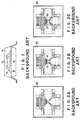
- FIGS. 2A, 2B and 2C show how mounting using such bedless type lead frames are conducted.
- a small pellet 12 is mounted on the central portion of the lead frame 20 shown in FIG. 2A through a small insulating sheet 16.
- a pellet 12′ larger than that in the case of FIG. 2B is mounted on the same portion as the above through a large insulating sheet 16′.
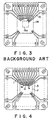
- FIG. 3 is a plan view in which the central portion of the bedless type lead frame shown in FIG. 2A is enlarged. A configuration is provided such that tip portions of respective inner leads 15a are substantially equidistant from the center of the lead frame.
- an object of this invention is to provide a semiconductor device capable of stably supporting an insulating sheet even at the central portion of a bedless lead frame.
- a semiconductor device comprising a plurality of inner leads substantially radially arranged around a pellet mounting portion, an insulating sheet arranged on the pellet mounting portion so as to adhesively fix inner lead tip portions and a semiconductor pellet mounted on the insulating sheet, in which each tip portion of at least every other inner lead is provided with a broader portion which is broader than the width of each of other inner lead tip portion, the tip portion of the broader portion is positioned closer to the central portion of the lead frame than other inner lead tip portions, and an opening or a thin portion is provided within the broader portion.
- the inner lead tip portions of the lead frame are formed broader at least at every other inner lead and since an opening or a thin portion for improving adhesive property of the insulating sheet is provided in each broader portion, the broader portion increases the contact surface to the insulating sheet, and the opening, etc. improves the bonding strength. Accordingly, even when a large number of inner leads are provided, it is possible to stably and firmly support the insulating sheet. In addition, since many kinds of semiconductor devices can be manufactured using the same lead frame in accordance with this invention, economical efficiency is also improved.
- FIG. 4 is an enlarged plan view showing a portion of a lead frame used for a semiconductor device according to an embodiment of this invention.
- inner leads 1 extend up to the portion in the vicinity of the central portion of the semiconductor device, and no bed portion is provided.
- Inner leads 1 under the insulating sheet 3 on which the pellet 2 is mounted as indicated by single-dotted lines are constructed as understood from FIG. 5 which is a plan view having an expansion rate greater than that of FIG. 4 in a manner that, e.g., the tip portion 1a of one inner lead and the tip portion 1b of the adjacent inner lead are different in the width and the position, i.e., the tip portion 1a is broader than the tip portion 1b and is positioned closer to the central portion of the lead frame than the latter.
- a circular opening 1c is provided in the broader tip portion 1a. The cross section of the opening 1c is shown in FIG. 6A.
- the broader portion 1a supports the insulating sheet at a position closer to the center of the lead frame and over a broad area, and bonding material is inserted into the opening 1c in bonding the insulating sheet, thus improving the bonding strength of the insulating sheet.
- thermosetting resin sheet is ordinarily used as the material satisfying these conditions.
- a paper into which thermosetting resin such as epoxy resin is impregnated may be also used.
- half-etching using an etchant may be also implemented onto the surface of the insulating sheet to form a thin portion 1d.
- FIG. 7 is a graph showing the effect obtained with this invention using a flat package of 44 pins wherein curve A shows the friction strength of the insulating sheet in the case of using a conventional lead frame, curve B shows the stripping strength of the insulating sheet in the case of using a lead frame having a tip formed as shown in FIG. 4 and including no opening, and curve C shows the stripping strength in the case of a lead frame having an opening shown in FIG. 6A. From this graph, it is seen that the bonding strength is considerably increased by the implementation of this invention.
- FIG. 6A shows a single opening in FIG. 6A or a single half-etching portion in FIG. 6B in the inner lead in the above-described embodiment, it may be provided in each lead.
- FIG. 6C shows the example where two half-etching portions ld are provided in one lead.
- broader lead tip portions are provided at every other lead in the above-described embodiment, they may be provided at intervals of two leads or more.
- arrangement density of broader lead tip portions may be changed depending upon places within the lead frame.
Landscapes
- Lead Frames For Integrated Circuits (AREA)
Applications Claiming Priority (2)
| Application Number | Priority Date | Filing Date | Title |
|---|---|---|---|
| JP319773/87 | 1987-12-17 | ||
| JP62319773A JPH01161743A (ja) | 1987-12-17 | 1987-12-17 | 半導体装置 |
Publications (3)
| Publication Number | Publication Date |
|---|---|
| EP0320997A2 true EP0320997A2 (de) | 1989-06-21 |
| EP0320997A3 EP0320997A3 (en) | 1989-10-18 |
| EP0320997B1 EP0320997B1 (de) | 1992-08-05 |
Family
ID=18114019
Family Applications (1)
| Application Number | Title | Priority Date | Filing Date |
|---|---|---|---|
| EP88121234A Expired - Lifetime EP0320997B1 (de) | 1987-12-17 | 1988-12-19 | Halbleiteranordnung mit einem Leiterrahmen |
Country Status (5)
| Country | Link |
|---|---|
| US (1) | US4949160A (de) |
| EP (1) | EP0320997B1 (de) |
| JP (1) | JPH01161743A (de) |
| KR (1) | KR910003543B1 (de) |
| DE (1) | DE3873500T2 (de) |
Cited By (3)
| Publication number | Priority date | Publication date | Assignee | Title |
|---|---|---|---|---|
| EP0405330A3 (en) * | 1989-06-29 | 1992-05-06 | Motorola, Inc. | Flagless leadframe, package and method |
| EP0588481A1 (de) * | 1992-08-17 | 1994-03-23 | American Microsystems, Incorporated | Bondflächen-Layout für IC-Halbleiterkörper und deren Herstellungsmethode |
| US5753977A (en) * | 1996-03-22 | 1998-05-19 | Mitsubishi Denki Kabushiki Kaisha | Semiconductor device and lead frame therefor |
Families Citing this family (8)
| Publication number | Priority date | Publication date | Assignee | Title |
|---|---|---|---|---|
| JPH0395661U (de) * | 1990-01-12 | 1991-09-30 | ||
| US5168345A (en) * | 1990-08-15 | 1992-12-01 | Lsi Logic Corporation | Semiconductor device having a universal die size inner lead layout |
| US5140404A (en) * | 1990-10-24 | 1992-08-18 | Micron Technology, Inc. | Semiconductor device manufactured by a method for attaching a semiconductor die to a leadframe using a thermoplastic covered carrier tape |
| US5177032A (en) * | 1990-10-24 | 1993-01-05 | Micron Technology, Inc. | Method for attaching a semiconductor die to a leadframe using a thermoplastic covered carrier tape |
| TW276357B (de) * | 1993-03-22 | 1996-05-21 | Motorola Inc | |
| US5714792A (en) * | 1994-09-30 | 1998-02-03 | Motorola, Inc. | Semiconductor device having a reduced die support area and method for making the same |
| JPH09199549A (ja) * | 1996-01-22 | 1997-07-31 | Denso Corp | ワイヤボンディング方法 |
| US7598599B2 (en) * | 2006-03-09 | 2009-10-06 | Stats Chippac Ltd. | Semiconductor package system with substrate having different bondable heights at lead finger tips |
Family Cites Families (4)
| Publication number | Priority date | Publication date | Assignee | Title |
|---|---|---|---|---|
| JPS5640265A (en) * | 1979-09-11 | 1981-04-16 | Nec Corp | Lead frame for semiconductor device |
| JPS60106158A (ja) * | 1983-11-14 | 1985-06-11 | Toshiba Corp | 半導体装置 |
| US4684975A (en) * | 1985-12-16 | 1987-08-04 | National Semiconductor Corporation | Molded semiconductor package having improved heat dissipation |
| US4721993A (en) * | 1986-01-31 | 1988-01-26 | Olin Corporation | Interconnect tape for use in tape automated bonding |
-
1987
- 1987-12-17 JP JP62319773A patent/JPH01161743A/ja active Granted
-
1988
- 1988-08-31 KR KR1019880011136A patent/KR910003543B1/ko not_active Expired
- 1988-12-16 US US07/285,021 patent/US4949160A/en not_active Expired - Lifetime
- 1988-12-19 DE DE8888121234T patent/DE3873500T2/de not_active Expired - Fee Related
- 1988-12-19 EP EP88121234A patent/EP0320997B1/de not_active Expired - Lifetime
Cited By (4)
| Publication number | Priority date | Publication date | Assignee | Title |
|---|---|---|---|---|
| EP0405330A3 (en) * | 1989-06-29 | 1992-05-06 | Motorola, Inc. | Flagless leadframe, package and method |
| EP0588481A1 (de) * | 1992-08-17 | 1994-03-23 | American Microsystems, Incorporated | Bondflächen-Layout für IC-Halbleiterkörper und deren Herstellungsmethode |
| US5753977A (en) * | 1996-03-22 | 1998-05-19 | Mitsubishi Denki Kabushiki Kaisha | Semiconductor device and lead frame therefor |
| DE19708002B4 (de) * | 1996-03-22 | 2004-09-16 | Mitsubishi Denki K.K. | Anschlußrahmen für Halbleiterbauelement |
Also Published As
| Publication number | Publication date |
|---|---|
| KR890011067A (ko) | 1989-08-12 |
| KR910003543B1 (ko) | 1991-06-04 |
| US4949160A (en) | 1990-08-14 |
| JPH0381308B2 (de) | 1991-12-27 |
| EP0320997B1 (de) | 1992-08-05 |
| DE3873500D1 (de) | 1992-09-10 |
| JPH01161743A (ja) | 1989-06-26 |
| DE3873500T2 (de) | 1993-02-11 |
| EP0320997A3 (en) | 1989-10-18 |
Similar Documents
| Publication | Publication Date | Title |
|---|---|---|
| EP0108502B1 (de) | Plastikverkapselte Halbleiteranordnung und ein Verfahren zu deren Herstellung | |
| US6002167A (en) | Semiconductor device having lead on chip structure | |
| US6229200B1 (en) | Saw-singulated leadless plastic chip carrier | |
| US6303985B1 (en) | Semiconductor lead frame and package with stiffened mounting paddle | |
| US5539251A (en) | Tie bar over chip lead frame design | |
| US6307257B1 (en) | Dual-chip integrated circuit package with a chip-die pad formed from leadframe leads | |
| US5358905A (en) | Semiconductor device having die pad locking to substantially reduce package cracking | |
| US4949160A (en) | Semiconductor device | |
| JPS62259450A (ja) | 集積回路ダイ・リ−ドフレ−ム相互接続組立体及び方法 | |
| US5479050A (en) | Leadframe with pedestal | |
| KR940012549A (ko) | 반도체 펙케지 | |
| US5168345A (en) | Semiconductor device having a universal die size inner lead layout | |
| US5780772A (en) | Solution to mold wire sweep in fine pitch devices | |
| US6376903B1 (en) | Semiconductor chip package with multilevel leads | |
| CN1114948C (zh) | 芯片上引线及标准常规引线的组合结构的半导体芯片封装 | |
| US5391923A (en) | Tape carrier including leads on both sides and resin-encapsulated semiconductor device incorporating the tape carrier | |
| WO2007018473A1 (en) | Leadframe and semiconductor package | |
| US6909179B2 (en) | Lead frame and semiconductor device using the lead frame and method of manufacturing the same | |
| JPS62150868A (ja) | 半導体装置用リ−ドフレ−ムとそれを使用する樹脂封止方法 | |
| US20020121682A1 (en) | Strapless lead frame | |
| JP2692442B2 (ja) | テープオートメイテッドボンディング方式大規模集積回路 | |
| KR0182509B1 (ko) | 연장된 타이 바를 갖는 리드 프레임과 그를 이용한 반도체 칩 패키지 | |
| JPH06140551A (ja) | 半導体装置 | |
| JPH031551A (ja) | 樹脂封止型半導体装置 | |
| KR0129004Y1 (ko) | 리드 프레임 |
Legal Events
| Date | Code | Title | Description |
|---|---|---|---|
| PUAI | Public reference made under article 153(3) epc to a published international application that has entered the european phase |
Free format text: ORIGINAL CODE: 0009012 |
|
| 17P | Request for examination filed |
Effective date: 19881219 |
|
| AK | Designated contracting states |
Kind code of ref document: A2 Designated state(s): DE FR GB IT |
|
| PUAL | Search report despatched |
Free format text: ORIGINAL CODE: 0009013 |
|
| AK | Designated contracting states |
Kind code of ref document: A3 Designated state(s): DE FR GB IT |
|
| 17Q | First examination report despatched |
Effective date: 19910515 |
|
| GRAA | (expected) grant |
Free format text: ORIGINAL CODE: 0009210 |
|
| AK | Designated contracting states |
Kind code of ref document: B1 Designated state(s): DE FR GB IT |
|
| ITF | It: translation for a ep patent filed | ||
| REF | Corresponds to: |
Ref document number: 3873500 Country of ref document: DE Date of ref document: 19920910 |
|
| ET | Fr: translation filed | ||
| PLBE | No opposition filed within time limit |
Free format text: ORIGINAL CODE: 0009261 |
|
| STAA | Information on the status of an ep patent application or granted ep patent |
Free format text: STATUS: NO OPPOSITION FILED WITHIN TIME LIMIT |
|
| 26N | No opposition filed | ||
| PGFP | Annual fee paid to national office [announced via postgrant information from national office to epo] |
Ref country code: GB Payment date: 19971210 Year of fee payment: 10 |
|
| PGFP | Annual fee paid to national office [announced via postgrant information from national office to epo] |
Ref country code: DE Payment date: 19971230 Year of fee payment: 10 |
|
| PG25 | Lapsed in a contracting state [announced via postgrant information from national office to epo] |
Ref country code: GB Free format text: LAPSE BECAUSE OF NON-PAYMENT OF DUE FEES Effective date: 19981219 |
|
| REG | Reference to a national code |
Ref country code: FR Ref legal event code: D6 |
|
| GBPC | Gb: european patent ceased through non-payment of renewal fee |
Effective date: 19981219 |
|
| PG25 | Lapsed in a contracting state [announced via postgrant information from national office to epo] |
Ref country code: DE Free format text: LAPSE BECAUSE OF NON-PAYMENT OF DUE FEES Effective date: 19991001 |
|
| PGFP | Annual fee paid to national office [announced via postgrant information from national office to epo] |
Ref country code: FR Payment date: 20051208 Year of fee payment: 18 |
|
| PG25 | Lapsed in a contracting state [announced via postgrant information from national office to epo] |
Ref country code: IT Free format text: LAPSE BECAUSE OF NON-PAYMENT OF DUE FEES Effective date: 20051219 |
|
| REG | Reference to a national code |
Ref country code: FR Ref legal event code: ST Effective date: 20070831 |
|
| PG25 | Lapsed in a contracting state [announced via postgrant information from national office to epo] |
Ref country code: FR Free format text: LAPSE BECAUSE OF NON-PAYMENT OF DUE FEES Effective date: 20070102 |