EP0321050A2 - Noeud de commutation d'un système de commutation à large bande - Google Patents
Noeud de commutation d'un système de commutation à large bande Download PDFInfo
- Publication number
- EP0321050A2 EP0321050A2 EP88202862A EP88202862A EP0321050A2 EP 0321050 A2 EP0321050 A2 EP 0321050A2 EP 88202862 A EP88202862 A EP 88202862A EP 88202862 A EP88202862 A EP 88202862A EP 0321050 A2 EP0321050 A2 EP 0321050A2
- Authority
- EP
- European Patent Office
- Prior art keywords
- switching
- input
- switching matrix
- blocks
- buffer
- Prior art date
- Legal status (The legal status is an assumption and is not a legal conclusion. Google has not performed a legal analysis and makes no representation as to the accuracy of the status listed.)
- Granted
Links
- 239000000872 buffer Substances 0.000 claims abstract description 109
- 239000011159 matrix material Substances 0.000 claims abstract description 90
- 230000005540 biological transmission Effects 0.000 claims abstract description 32
- 238000000034 method Methods 0.000 claims description 18
- 239000004744 fabric Substances 0.000 claims 1
- 238000013461 design Methods 0.000 abstract description 2
- 238000011161 development Methods 0.000 abstract description 2
- 238000012546 transfer Methods 0.000 description 7
- 230000001360 synchronised effect Effects 0.000 description 6
- 230000003139 buffering effect Effects 0.000 description 4
- 230000008878 coupling Effects 0.000 description 4
- 238000010168 coupling process Methods 0.000 description 4
- 238000005859 coupling reaction Methods 0.000 description 4
- 230000008569 process Effects 0.000 description 4
- 238000005516 engineering process Methods 0.000 description 3
- 230000001934 delay Effects 0.000 description 2
- 238000011835 investigation Methods 0.000 description 2
- 239000004065 semiconductor Substances 0.000 description 2
- 230000008901 benefit Effects 0.000 description 1
- 230000002457 bidirectional effect Effects 0.000 description 1
- 230000008859 change Effects 0.000 description 1
- 238000004891 communication Methods 0.000 description 1
- 230000008094 contradictory effect Effects 0.000 description 1
- 238000010586 diagram Methods 0.000 description 1
- 230000006872 improvement Effects 0.000 description 1
- 238000012432 intermediate storage Methods 0.000 description 1
- 239000012464 large buffer Substances 0.000 description 1
- 230000015654 memory Effects 0.000 description 1
- 230000003287 optical effect Effects 0.000 description 1
- 238000011056 performance test Methods 0.000 description 1
- 238000012545 processing Methods 0.000 description 1
- 230000007704 transition Effects 0.000 description 1
Images


Classifications
-
- H—ELECTRICITY
- H04—ELECTRIC COMMUNICATION TECHNIQUE
- H04L—TRANSMISSION OF DIGITAL INFORMATION, e.g. TELEGRAPHIC COMMUNICATION
- H04L49/00—Packet switching elements
- H04L49/30—Peripheral units, e.g. input or output ports
-
- H—ELECTRICITY
- H04—ELECTRIC COMMUNICATION TECHNIQUE
- H04L—TRANSMISSION OF DIGITAL INFORMATION, e.g. TELEGRAPHIC COMMUNICATION
- H04L49/00—Packet switching elements
- H04L49/15—Interconnection of switching modules
- H04L49/1553—Interconnection of ATM switching modules, e.g. ATM switching fabrics
-
- H—ELECTRICITY
- H04—ELECTRIC COMMUNICATION TECHNIQUE
- H04L—TRANSMISSION OF DIGITAL INFORMATION, e.g. TELEGRAPHIC COMMUNICATION
- H04L49/00—Packet switching elements
- H04L49/30—Peripheral units, e.g. input or output ports
- H04L49/3081—ATM peripheral units, e.g. policing, insertion or extraction
-
- H—ELECTRICITY
- H04—ELECTRIC COMMUNICATION TECHNIQUE
- H04L—TRANSMISSION OF DIGITAL INFORMATION, e.g. TELEGRAPHIC COMMUNICATION
- H04L49/00—Packet switching elements
- H04L49/50—Overload detection or protection within a single switching element
- H04L49/505—Corrective measures
- H04L49/508—Head of Line Blocking Avoidance
-
- H—ELECTRICITY
- H04—ELECTRIC COMMUNICATION TECHNIQUE
- H04L—TRANSMISSION OF DIGITAL INFORMATION, e.g. TELEGRAPHIC COMMUNICATION
- H04L49/00—Packet switching elements
- H04L49/15—Interconnection of switching modules
- H04L49/1515—Non-blocking multistage, e.g. Clos
- H04L49/1523—Parallel switch fabric planes
Definitions
- the invention relates to a switching matrix for a switching node of a broadband switching system according to the preamble of claims 1 to 5.
- Packet switching packet switching
- the (digital) messages are divided into packets, each packet containing additional information in addition to the useful information, which includes Include information about the destination (address).
- messages can be directed to the partner involved in the connection on the basis of their packet addresses, which only requires transmission capacity if a message is actually to be transmitted.
- circuit switching has been known for a long time, which requires transmission capacity for the entire duration of the connection - regardless of whether messages are being transmitted or not.
- bidirectional transmission paths are made available, although in general only one of the two telephone subscribers speaks.
- the use of packet switching for data traffic has resulted in throughput rates of the order of 1 to 1000 packets per second and above.
- throughput rates of the order of 1 to 1000 packets per second and above.
- Services using the packet switching method for example in image communication, are already expected to be thousands of times larger.
- ATM Asynchronous Transfer Mode
- the incoming data packets are processed decentrally by receiving internal address information according to their destination, connecting them through the central switching network and then forwarding them at the exit without the internal address information.
- Embodiments of the "ATM” are "Asynchronous Time Division (ATD)” and “Fast Packet Switching (FPS)".
- Asynchronous transfer mode a specific transmission channel is identified solely by its time interval from a synchronous word.
- Asynchronous Transfer Mode the respective channel is identified by the addresses (headers) of its packets (blocks), in particular the beginning of the blocks can be recognized so that the headers can be evaluated. Flags or an underlying synchronous structure that requires a constant block length are used for this.
- An example of this is "Asynchronous Time Division”, in which synchronous words are repeatedly shown as "empty blocks” in the bit stream.
- broadband networks depends on many factors, including standardization, low-cost optical broadband transmission, VLSI circuits for very high processing speeds, and the demands of users and network operators.
- the conception of such broadband networks is based on the recently created ISDN integrated service network.
- a first possibility for expanding the integrated telecommunications network ISDN is to provide a limited number of broadband channels, with a physical connection being established for each broadband channel.
- the network created by means of circuit switching does not meet all the requirements of the network operator for an adaptable network for the transmission of all possible services, including services with parameters that have not yet been standardized internationally, and for future services.
- a broadband switching system in which the message is broken down into blocks (cells) and transmitted over broadband transmission paths according to an asynchronous time division method.
- the blocks (cells) can have the same or different lengths.
- the blocks consist of user and address information, the address information being accommodated in a so-called message header.
- the number of bits in a block is referred to as its length, with values between 120 and 256 bits being provided for the useful information and 32 or 16 bits for the header in the standardization proposals.
- the time intervals in which blocks are transmitted are called frames draws. A frame can contain a valid block or be empty.
- the switching nodes can be centrally buffered systems (as known for example from the European patent application with the publication number 0 183 592) or decentrally buffered systems.
- centrally buffered systems there is only one buffer, in which each incoming line stores its incoming blocks and from which each outgoing line reads out certain blocks again.
- Systems with decentralized buffering are further differentiated as to whether blocks are buffered exclusively on the input side (an embodiment for this is described, for example, in the unpublished German patent application with the official file number P 37 14 385.9) or whether the buffers are only in front of the outgoing lines (see, for example, IEEE, B 10.2.1, 1987, "The Knockout Switch: A Simple, Modular Architecture for High-Performance Packet Switching by JS Yeh et al) are arranged or whether they are systems with input and output buffering.
- the switching node has the task of establishing connections between the participants in the broadband switching system, which is characterized as follows: - The information must be in digital form, analog data may need to be digitized. - The information in digital form is divided into blocks of equal length. - The blocks are - provided with a message header (header) of length h bits - to a switching node. - Depending on their destination, the latter forwards the blocks to other switching nodes until one of these nodes can deliver the block to the desired end user. - The header of a block may be changed (implemented) by a node. - The blocks are transmitted in a fixed time frame in which there is time for the transmission of a block.
- the length of a block is measured in bits, the duration of a time frame is therefore the cycle time times the total block length.
- the switching nodes must synchronize with the beginning of a time frame. Since a larger network cannot work completely synchronously, the connection line between two nodes - also called the long-distance line - must be synchronized. The switching nodes themselves have to adapt the external clock to their internal clock by buffering.
- waiting buffers must be provided when implementing a switching matrix.
- the waiting buffers can be located on the input side at the crossing points of the coupling matrix or on the output side.
- Such a coupling matrix is the least expensive if the buffers only have to be installed on the input or only on the output side.
- the header must be kept very short, so that a number of e.g. can be handed over to several million participants. For this reason, only two virtual connections are established for each participant: the header is therefore only defined for one connection. It turns out that it is best if a block on each trunk between two nodes always receives a new header. This means that each header must first be converted before the block can be transferred to the trunk line on which it is to be forwarded. Sufficient time must be made available for this implementation and for the determination of the outgoing long-distance line.
- Two blocks conflict with each other if the same circuit parts are to be used for the transmission. As a rule, one of the blocks is then prioritized over the other, and the other block either has to wait or is lost.
- a block B In the case of the disability, a block B must wait for the operation of a block A, but at the same time A is not operated because a conflict between block A and a third block C occurs.
- a normal wait situation in a wait buffer is not a hindrance as long as the first block in the buffer is transmitted in every frame clock. Only when this comes into conflict and is not served, but also at the same time no other block in this wait buffer can be transferred, an obstruction occurs.
- the concept of disability is important for the performance assessment of such systems. Because if a non-empty wait buffer cannot be processed during a frame time, one can imagine that an additional "virtual" block is processed instead. The sum of the virtual and real load then gives the total load on the system. The virtual load can be almost as large as the real load for some switching networks. This applies above all to switching matrixes that use input buffering.
- the invention has for its object to provide a switching matrix for a switching node of a broadband switching system in such a way that the occurrence of service bottlenecks in the switching matrix is largely avoided.
- the switching matrixes according to claims 1 to 5 have the advantage that the transmission rate of the switching matrix is increased in a simple manner, with no major delays in the connection of the blocks in the switching matrix and the occurrence of conflicts is largely avoided.
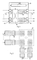
- FIG. 1 shows the basic structure of a switching node VK in a broadband switching system in which the messages are broken down into blocks.
- the blocks are transmitted over broadband transmission paths of the broadband switching system using an asynchronous time division method.
- the blocks received by its input circuits ES connected to input lines EL are temporarily stored in the switching node VK before being forwarded to its output circuit AS.
- 1 shows the intermediate storage of the blocks in output buffers AP connected to a switching matrix KF.
- blocks can be transferred from several input lines EL to several output lines AL switch.
- a coupling device is described, which can establish a connection between an input line EL and any output line AL for the time the transmission of a block.
- the traffic performance of a general switching system is limited by the occurrence of conflicts. This happens when blocks for the same output line AL are offered on two or more of the input lines EL. Since each output line AL can only take up one block, the non-removable blocks on the input line EL are impeded. So that they are not lost, they must be buffered. The memories used for this have only a finite capacity. It was investigated at which load on the input lines EL with blocks such a large backlog occurs that incoming blocks can be lost because the buffer space in the waiting buffer (eg input buffer) is not sufficient for them.
- the boundary conditions resulting from the performance tests are changed so that no major delays and losses of the Blocks can arise.
- This can be done in several ways or combinations thereof: -
- the transmission rate of the switching matrix can be increased by structural changes -
- the switching matrix can be multiplied -
- the input buffers can be reorganized -
- the allocation strategy can be changed.
- the performance of the broadband switching system can be increased in that the switching matrix can switch faster. This can be achieved by using faster technology, which, however, does not yet appear to be possible with current semiconductor technology. Structural measures must therefore be taken to achieve faster switching of the switching matrix.
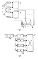
- FIG. 2 shows a switching matrix KF in which the transmission of the blocks in the switching matrix KF takes place bit-parallel, whereby the transition time of the blocks in the switching matrix KF is reduced and the probability of conflicts occurring is reduced.
- bit-parallel transmission instead of one, several lines are switched through in each crossing point of the switching device and the blocks are broken down into sub-blocks corresponding to a large number of bits.
- more than one block can arrive at an output circuit AS during the time in which a block can be placed on a trunk line. It follows that these blocks have to be buffered additionally.
- integrated waiting buffers e.g. input buffer EP or output buffer AP
- input buffer EP or output buffer AP usually have a clock rate that is significantly lower than that of the long-distance lines, it would also make sense here to buffer the blocks in parallel. This would reduce the time it takes to clock one block further, depending on the degree of parallelization.
- the switching matrix itself can also be multiplied.
- a switch distributes the incoming blocks evenly over the individual switching matrixes KF, so that their load remains below a critical limit.
- the blocks which are provided for the same output line AL are stored in a common buffer until output.
- a waiting buffer must also be provided at the output, which must additionally have the property of being able to accommodate more than one block at the same time. Since this may be technically difficult, a separate buffer AP1, AP2 was provided for each switching matrix KF and each output circuit AS in the embodiment shown in FIG. The output circuit AS then selects a block from all the buffers AP1, AP2 assigned to it, which can be done using an n: 1 multiplexer. However, this procedure reduces the otherwise usable bundling gain of the waiting buffers. It is also one Combination of both methods with several short input buffers and a longer shared wait buffer is conceivable.
- FIGS. 5a and 5b show that increasing the buffer access depth to 2 blocks increases the system's load capacity by approximately 14%. Therefore, this measure brings about a significant improvement in the performance of the system, without causing problems in the switching matrixes according to FIG. 2 or FIG. 3 with the output buffers AP or blocks which overtake each other.
- the waiting buffer is used to increase the buffer access depth in the input buffer EP and intermediate buffer ZSP broken down, which should only be regarded as logically separated from the input buffer EP; they can be part of this buffer.
- a block in buffer A is placed on the switching matrix KF when it can remove the block. If it cannot take it over, the block is instead put into the intermediate buffer B. In both cases, the next block X is clocked from the input buffer EP into the intermediate buffer A. This happens as long as there is a free intermediate buffer ZSP. Then the input buffer control EPST waits until a block could be issued. Since it can now offer four blocks to the system, the probability of this is very high. This relationship is shown in the table below for a buffer access depth of 4.
- a decision logic ensures that all blocks in the intermediate buffers ZSP of an input circuit ES are passed on to the switching matrix KF in the correct order.
- the decision logic comprises so-called partial switching matrix controllers KFST and input buffer controllers EPST.
- the partial switching matrix controller KFST has a selection cycle circuit ASZ, which is connected via a line with the control signal S or S 'to the previous and subsequent partial switching matrix controller KFST.
- the selection cycle circuit ASZ is connected to the output of an OR gate O and an input of an AND gate U.
- the two inputs of the OR gate O and the second input of the AND gate U are connected to the input buffer control EPST with an increased buffer access depth.
- the partial switching matrix controller KFST stores the information as to which input buffer EP was last connected to the output buffer AP assigned to this partial switching matrix controller KFST. In the event that a plurality of input buffers EP are to be connected to the output buffer AP assigned to the partial switching matrix controller KFST, the partial switching matrix controller KFST selects that input buffer EP which is in a fixed selection cycle between all input buffers EP behind the last read input buffer EP.
- the selection cycle is determined, for example, by the spatial arrangement of the input buffers EP.
- the decision logic therefore chooses from all input circuits ES, which want to send to the same output circuits AS, an input circuit ES. This happens cyclically.
- 7 shows an embodiment for a switching matrix control.
- the partial switching matrix controller KFST contains a D flip-flop DF, in which the information about which input buffer EP was last connected to the output buffer AP assigned to this partial switching matrix controller KFST is stored.
- the input buffer EP is connected to a first input of a first AND gate U1, a first input of a first OR gate O1 and the input of an inverter I.
- the output of the inverter I is present at a first input of a second AND gate U2.
- the preceding sub-switching matrix controller KFST is connected to the second input of the second AND gate U2 and the first input of a third AND gate U3 in order to supply a control signal S.
- the second output of the third AND gate U3 is connected to the output of the first OR gate O1 and the output of the third AND gate U3 is connected to the D input of the D flip-flop DF.
- the Q output of the D flip-flop DF is connected to the first input of a second OR gate O2, to the second input of the first OR gate O1 and to the second input of the first AND gate U1.
- the output of the second AND gate U2 is connected to the second input of the third OR gate O3.
- the output of the first AND gate U1 is connected to the input buffer EP and the subsequent sub-switching control unit KFST is connected to the output of the third OR gate O3.
- the D flip-flop DF stores which input circuit ES last sent. This now has the lowest priority.
- the decision logic selects the next coming input circuit ES in the cycle, which wants to send a block to this output circuit AS. Its D flip-flop DF is set, the old one is deleted, and by sending the read signal A, this input circuit ES is informed that it can send a block.
- a signal is formed in the input buffer control EPST for all intermediate buffers ZSP, which signals the decision logic that one of the intermediate buffers ZSP of this input circuit ES wants to send to this output circuit AS. As soon as this line is released (by sending the read signal A), the first block (furthest forward in the buffer) is selected. This can then be placed on this output circuit AS.
- the number of input lines of the switching matrix KF is increased (fourfold). It is also possible to increase the number of output lines of the switching matrix KF and to assign several lines in the switching matrix KF to each outgoing trunk line. Again, it is necessary here that waiting buffers must also be provided in the output circuit AS, since the access rate of blocks can briefly exceed the maximum transmission rate. The performance of such a switching matrix hardly differs from that of a switching matrix according to FIG. 4, which however does not require an output buffer AP.
- This switching matrix control (decision logic) can also be applied to the subject of P 37 14 385.9.
- Each input circuit ES should have a different priority through different output circuits AS, for example in the following form with 16 input and output circuits: exit Falling priority of input circuits -1 : 1 2nd 3rd 4th 5 6 7 8th 9 10th 11 12 13 14 15 16 -2: 2nd 3rd 4th 5 6 7 8th 9 10th 11 12 13 14 15 16 1 -3: 3rd 4th 5 6 7 8th 9 10th 11 12 13 14 15 16 1 2nd ; ... ... ... ... ... ... ... ... ... ... ... ... ... ... ... -16: 16 1 2nd 3rd 4th 5 6 7 8th 9 10th 11 12 13 14 15
Landscapes
- Engineering & Computer Science (AREA)
- Computer Networks & Wireless Communication (AREA)
- Signal Processing (AREA)
- Data Exchanges In Wide-Area Networks (AREA)
Applications Claiming Priority (2)
| Application Number | Priority Date | Filing Date | Title |
|---|---|---|---|
| DE19873742748 DE3742748A1 (de) | 1987-12-17 | 1987-12-17 | Koppelfeld und koppelfeldsteuerung fuer einen vermittlungsknoten eines breitband-vermittlungssystems |
| DE3742748 | 1987-12-17 |
Publications (3)
| Publication Number | Publication Date |
|---|---|
| EP0321050A2 true EP0321050A2 (fr) | 1989-06-21 |
| EP0321050A3 EP0321050A3 (fr) | 1992-07-01 |
| EP0321050B1 EP0321050B1 (fr) | 1995-03-22 |
Family
ID=6342800
Family Applications (1)
| Application Number | Title | Priority Date | Filing Date |
|---|---|---|---|
| EP88202862A Expired - Lifetime EP0321050B1 (fr) | 1987-12-17 | 1988-12-13 | Noeud de commutation d'un système de commutation à large bande |
Country Status (3)
| Country | Link |
|---|---|
| EP (1) | EP0321050B1 (fr) |
| JP (1) | JP2752116B2 (fr) |
| DE (2) | DE3742748A1 (fr) |
Cited By (5)
| Publication number | Priority date | Publication date | Assignee | Title |
|---|---|---|---|---|
| EP0453606A1 (fr) * | 1990-04-27 | 1991-10-30 | Siemens Aktiengesellschaft | Méthode et dispositif pour réduire la perte de paquets d'information, transmis par un commutateur de paquets |
| EP0453607A1 (fr) * | 1990-04-27 | 1991-10-30 | Siemens Aktiengesellschaft | Méthode et dispositif pour réduire la perte de paquets d'information, transmis par un commutateur de paquets |
| EP0410139A3 (en) * | 1989-06-22 | 1992-06-03 | Fujitsu Limited | Atm switching system having dual atm switch structure |
| EP0455827A4 (en) * | 1989-11-29 | 1992-10-21 | Fujitsu Limited | Changing over method for doubled atm switch system |
| EP0641107A3 (fr) * | 1993-07-30 | 1996-11-06 | Nec Corp | Système de commutation de cellules ATM. |
Families Citing this family (1)
| Publication number | Priority date | Publication date | Assignee | Title |
|---|---|---|---|---|
| SE515177C2 (sv) * | 1992-06-01 | 2001-06-25 | Ericsson Telefon Ab L M | Kvadratisk väljararkitektur |
Family Cites Families (5)
| Publication number | Priority date | Publication date | Assignee | Title |
|---|---|---|---|---|
| FR2538976A1 (fr) * | 1982-12-29 | 1984-07-06 | Servel Michel | Systeme de commutation de paquets synchrones de longueur fixe |
| FR2538984A1 (fr) * | 1982-12-30 | 1984-07-06 | Devault Michel | Commutateur pour reseau numerique multidebit a commutation temporelle asynchrone adapte aux videocommutations |
| FR2572871B1 (fr) * | 1984-11-08 | 1987-01-23 | Labo Cent Telecommunicat | Commutateur de paquets asynchrone |
| JPS61216545A (ja) * | 1985-02-14 | 1986-09-26 | Fujitsu Ltd | 高速パケツト交換方式 |
| US4914652A (en) * | 1988-08-01 | 1990-04-03 | Advanced Micro Devices, Inc. | Method for transfer of data between a media access controller and buffer memory in a token ring network |
-
1987
- 1987-12-17 DE DE19873742748 patent/DE3742748A1/de not_active Withdrawn
-
1988
- 1988-12-13 DE DE3853412T patent/DE3853412D1/de not_active Expired - Fee Related
- 1988-12-13 EP EP88202862A patent/EP0321050B1/fr not_active Expired - Lifetime
- 1988-12-16 JP JP31656088A patent/JP2752116B2/ja not_active Expired - Fee Related
Cited By (8)
| Publication number | Priority date | Publication date | Assignee | Title |
|---|---|---|---|---|
| EP0410139A3 (en) * | 1989-06-22 | 1992-06-03 | Fujitsu Limited | Atm switching system having dual atm switch structure |
| EP0455827A4 (en) * | 1989-11-29 | 1992-10-21 | Fujitsu Limited | Changing over method for doubled atm switch system |
| US5274633A (en) * | 1989-11-29 | 1993-12-28 | Fujitsu Limited | Switching system for ATM dual switch system |
| EP0453606A1 (fr) * | 1990-04-27 | 1991-10-30 | Siemens Aktiengesellschaft | Méthode et dispositif pour réduire la perte de paquets d'information, transmis par un commutateur de paquets |
| EP0453607A1 (fr) * | 1990-04-27 | 1991-10-30 | Siemens Aktiengesellschaft | Méthode et dispositif pour réduire la perte de paquets d'information, transmis par un commutateur de paquets |
| US5200950A (en) * | 1990-04-27 | 1993-04-06 | Siemens Aktiengesellschaft | Method and circuit arrangement for reducing the loss of message packets that are transmitted via a packet switching equipment |
| US5222063A (en) * | 1990-04-27 | 1993-06-22 | Siemens Aktiengesellschaft | Method and circuit arrangement for reducing the loss of message packets that are transmitted via a packet switching equipment |
| EP0641107A3 (fr) * | 1993-07-30 | 1996-11-06 | Nec Corp | Système de commutation de cellules ATM. |
Also Published As
| Publication number | Publication date |
|---|---|
| JPH022766A (ja) | 1990-01-08 |
| EP0321050B1 (fr) | 1995-03-22 |
| DE3742748A1 (de) | 1989-07-06 |
| EP0321050A3 (fr) | 1992-07-01 |
| DE3853412D1 (de) | 1995-04-27 |
| JP2752116B2 (ja) | 1998-05-18 |
Similar Documents
| Publication | Publication Date | Title |
|---|---|---|
| DE3751046T2 (de) | Vermittlungssystem. | |
| EP0276776B1 (fr) | Réseau numérique de commutation pour la commutation en circuit et en paquet, et matrice de couplage correspondante | |
| DE69003950T2 (de) | Schaltknoten für ein kommunikationsschaltnetz. | |
| DE69520229T2 (de) | ATM-VERMITTLUNGSSTELLE mit höher Kapazität | |
| DE69900492T2 (de) | Grosse kombinierte Breitband und Schmalband Vermittlungsstelle | |
| DE69124645T2 (de) | Verfahren und Schaltung zur Verkehrsformung | |
| DE60119866T2 (de) | Vermittlungseinrichtung und verfahren mit getrennten Ausgangspuffern | |
| DE3856469T2 (de) | Selbstsuchendes vermittlungssystem | |
| DE69033231T2 (de) | Erweitbare Paketvermittlungsarchitektur | |
| DE69020578T2 (de) | Grundelement für ein verbindungsnetzwerk eines knotens zur schnellen paketvermittlung. | |
| DE3788605T2 (de) | Paketvermittlung. | |
| DE3788606T2 (de) | Anordnung zur Überwachung von Steuerinformation für ein Vermittlungssystem mit verteilter Steuerung. | |
| DE69033213T2 (de) | Verbindungsstruktur zur Verbindung zwischen einem Eingang und willkürlichen Ausgängen aus einer Gruppe von Ausgängen | |
| DE19531749A1 (de) | Verkehrsgestaltungseinrichtung und Paket-Kommunikationsgerät | |
| DE3788911T2 (de) | Verteiltes Paketvermittlungssystem. | |
| EP0289087B1 (fr) | Système de commutation par paquets | |
| EP0351014B1 (fr) | Réseau de commutation pour système de commutation | |
| DE69219390T2 (de) | ATM-Zellenvermittlungssystem | |
| EP0453607A1 (fr) | Méthode et dispositif pour réduire la perte de paquets d'information, transmis par un commutateur de paquets | |
| EP0321050B1 (fr) | Noeud de commutation d'un système de commutation à large bande | |
| DE69216355T2 (de) | Vermittlungsverfahren und Koppelfeldeinrichtung mit einem gemeinsamen Pufferspeicher | |
| EP0322075B1 (fr) | Réseau de commutation et dispositif de commande pour un système de commutation | |
| DE69521029T2 (de) | Vermittlungsvorrichtung | |
| EP0557849A2 (fr) | Méthode de transmission des données en paquets sur le canal D dans un central privé RNIS | |
| EP0443672B1 (fr) | Système à mode de transfert asynchrone |
Legal Events
| Date | Code | Title | Description |
|---|---|---|---|
| PUAI | Public reference made under article 153(3) epc to a published international application that has entered the european phase |
Free format text: ORIGINAL CODE: 0009012 |
|
| AK | Designated contracting states |
Kind code of ref document: A2 Designated state(s): DE FR GB IT SE |
|
| PUAL | Search report despatched |
Free format text: ORIGINAL CODE: 0009013 |
|
| AK | Designated contracting states |
Kind code of ref document: A3 Designated state(s): DE FR GB IT SE |
|
| 17P | Request for examination filed |
Effective date: 19921221 |
|
| 17Q | First examination report despatched |
Effective date: 19931207 |
|
| RHK1 | Main classification (correction) |
Ipc: H04L 12/42 |
|
| RHK1 | Main classification (correction) |
Ipc: H04L 12/42 |
|
| GRAA | (expected) grant |
Free format text: ORIGINAL CODE: 0009210 |
|
| AK | Designated contracting states |
Kind code of ref document: B1 Designated state(s): DE FR GB IT SE |
|
| PG25 | Lapsed in a contracting state [announced via postgrant information from national office to epo] |
Ref country code: IT Free format text: LAPSE BECAUSE OF FAILURE TO SUBMIT A TRANSLATION OF THE DESCRIPTION OR TO PAY THE FEE WITHIN THE PRE;WARNING: LAPSES OF ITALIAN PATENTS WITH EFFECTIVE DATE BEFORE 2007 MAY HAVE OCCURRED AT ANY TIME BEFORE 2007. THE CORRECT EFFECTIVE DATE MAY BE DIFFERENT FROM THE ONE RECORDED.SCRIBED TIME-LIMIT Effective date: 19950322 |
|
| REF | Corresponds to: |
Ref document number: 3853412 Country of ref document: DE Date of ref document: 19950427 |
|
| ET | Fr: translation filed | ||
| GBT | Gb: translation of ep patent filed (gb section 77(6)(a)/1977) |
Effective date: 19950626 |
|
| PLBE | No opposition filed within time limit |
Free format text: ORIGINAL CODE: 0009261 |
|
| STAA | Information on the status of an ep patent application or granted ep patent |
Free format text: STATUS: NO OPPOSITION FILED WITHIN TIME LIMIT |
|
| 26N | No opposition filed | ||
| REG | Reference to a national code |
Ref country code: FR Ref legal event code: CD |
|
| REG | Reference to a national code |
Ref country code: GB Ref legal event code: IF02 |
|
| REG | Reference to a national code |
Ref country code: GB Ref legal event code: 746 Effective date: 20020918 |
|
| REG | Reference to a national code |
Ref country code: FR Ref legal event code: D6 |
|
| PGFP | Annual fee paid to national office [announced via postgrant information from national office to epo] |
Ref country code: FR Payment date: 20021223 Year of fee payment: 15 |
|
| PGFP | Annual fee paid to national office [announced via postgrant information from national office to epo] |
Ref country code: GB Payment date: 20021224 Year of fee payment: 15 |
|
| PGFP | Annual fee paid to national office [announced via postgrant information from national office to epo] |
Ref country code: SE Payment date: 20021227 Year of fee payment: 15 |
|
| PGFP | Annual fee paid to national office [announced via postgrant information from national office to epo] |
Ref country code: DE Payment date: 20030217 Year of fee payment: 15 |
|
| PG25 | Lapsed in a contracting state [announced via postgrant information from national office to epo] |
Ref country code: GB Free format text: LAPSE BECAUSE OF NON-PAYMENT OF DUE FEES Effective date: 20031213 |
|
| PG25 | Lapsed in a contracting state [announced via postgrant information from national office to epo] |
Ref country code: SE Free format text: LAPSE BECAUSE OF NON-PAYMENT OF DUE FEES Effective date: 20031214 |
|
| PG25 | Lapsed in a contracting state [announced via postgrant information from national office to epo] |
Ref country code: DE Free format text: LAPSE BECAUSE OF NON-PAYMENT OF DUE FEES Effective date: 20040701 |
|
| EUG | Se: european patent has lapsed | ||
| GBPC | Gb: european patent ceased through non-payment of renewal fee |
Effective date: 20031213 |
|
| PG25 | Lapsed in a contracting state [announced via postgrant information from national office to epo] |
Ref country code: FR Free format text: LAPSE BECAUSE OF NON-PAYMENT OF DUE FEES Effective date: 20040831 |
|
| REG | Reference to a national code |
Ref country code: FR Ref legal event code: ST |