EP0321250A2 - Dispositif de mémoire magnéto-optique - Google Patents
Dispositif de mémoire magnéto-optique Download PDFInfo
- Publication number
- EP0321250A2 EP0321250A2 EP88311888A EP88311888A EP0321250A2 EP 0321250 A2 EP0321250 A2 EP 0321250A2 EP 88311888 A EP88311888 A EP 88311888A EP 88311888 A EP88311888 A EP 88311888A EP 0321250 A2 EP0321250 A2 EP 0321250A2
- Authority
- EP
- European Patent Office
- Prior art keywords
- film
- substrate
- magneto
- optic
- alloy
- Prior art date
- Legal status (The legal status is an assumption and is not a legal conclusion. Google has not performed a legal analysis and makes no representation as to the accuracy of the status listed.)
- Granted
Links
Images
Classifications
-
- G—PHYSICS
- G11—INFORMATION STORAGE
- G11B—INFORMATION STORAGE BASED ON RELATIVE MOVEMENT BETWEEN RECORD CARRIER AND TRANSDUCER
- G11B11/00—Recording on or reproducing from the same record carrier wherein for these two operations the methods are covered by different main groups of groups G11B3/00 - G11B7/00 or by different subgroups of group G11B9/00; Record carriers therefor
- G11B11/10—Recording on or reproducing from the same record carrier wherein for these two operations the methods are covered by different main groups of groups G11B3/00 - G11B7/00 or by different subgroups of group G11B9/00; Record carriers therefor using recording by magnetic means or other means for magnetisation or demagnetisation of a record carrier, e.g. light induced spin magnetisation; Demagnetisation by thermal or stress means in the presence or not of an orienting magnetic field
- G11B11/105—Recording on or reproducing from the same record carrier wherein for these two operations the methods are covered by different main groups of groups G11B3/00 - G11B7/00 or by different subgroups of group G11B9/00; Record carriers therefor using recording by magnetic means or other means for magnetisation or demagnetisation of a record carrier, e.g. light induced spin magnetisation; Demagnetisation by thermal or stress means in the presence or not of an orienting magnetic field using a beam of light or a magnetic field for recording by change of magnetisation and a beam of light for reproducing, i.e. magneto-optical, e.g. light-induced thermomagnetic recording, spin magnetisation recording, Kerr or Faraday effect reproducing
- G11B11/10582—Record carriers characterised by the selection of the material or by the structure or form
- G11B11/10586—Record carriers characterised by the selection of the material or by the structure or form characterised by the selection of the material
- G11B11/10589—Details
- G11B11/10593—Details for improving read-out properties, e.g. polarisation of light
-
- G—PHYSICS
- G11—INFORMATION STORAGE
- G11B—INFORMATION STORAGE BASED ON RELATIVE MOVEMENT BETWEEN RECORD CARRIER AND TRANSDUCER
- G11B11/00—Recording on or reproducing from the same record carrier wherein for these two operations the methods are covered by different main groups of groups G11B3/00 - G11B7/00 or by different subgroups of group G11B9/00; Record carriers therefor
- G11B11/10—Recording on or reproducing from the same record carrier wherein for these two operations the methods are covered by different main groups of groups G11B3/00 - G11B7/00 or by different subgroups of group G11B9/00; Record carriers therefor using recording by magnetic means or other means for magnetisation or demagnetisation of a record carrier, e.g. light induced spin magnetisation; Demagnetisation by thermal or stress means in the presence or not of an orienting magnetic field
- G11B11/105—Recording on or reproducing from the same record carrier wherein for these two operations the methods are covered by different main groups of groups G11B3/00 - G11B7/00 or by different subgroups of group G11B9/00; Record carriers therefor using recording by magnetic means or other means for magnetisation or demagnetisation of a record carrier, e.g. light induced spin magnetisation; Demagnetisation by thermal or stress means in the presence or not of an orienting magnetic field using a beam of light or a magnetic field for recording by change of magnetisation and a beam of light for reproducing, i.e. magneto-optical, e.g. light-induced thermomagnetic recording, spin magnetisation recording, Kerr or Faraday effect reproducing
- G11B11/10582—Record carriers characterised by the selection of the material or by the structure or form
Definitions
- the present invention relates to magneto-optic memory devices, and more particularly to magneto-optic memory devices, such as magneto-optic discs and magneto-optic cards, which are adapted to record data thereon and reproduce or erase the data therefrom when exposed, for example, to a laser beam.
- magneto-optic memory devices as optical memory devices adapted for recording, reproducing and erasing data.
- a rare earth-transition metal alloy thin film is used as the memory medium because the recording bits are free of the influence of the grain boundary and further because the film serving as the memory medium can be formed over a large area relatively easily.
- the magneto-optic memory devices incorporating the rare earth-transition metal alloy thin film as the memory medium generally fail to exhibit satisfactory magneto optic effects (Kerr effect and Faraday effect) and therefore still remain to be improved in the S/N ratio of reproduction signals.
- the so-called reflective film structure is employed for magneto-optic memory devices as already disclosed, for example, in Unexamined Japanese Patent Publication SHO 57-12428 and Applied Optics, Vol. 28, No. 22, p. 3927.
- Fig. 3 is a view partly in vertical section and showing a conventional magneto-optic memory device of reflective film structure.
- indicated at a is a transparent substrate of glass, polycarbonate resin, epoxy resin or the like, at b a transparent dielectric film having a higher refractive index than the substrate a , at c a rare earth-transition metal alloy thin film, at d a transparent dielectric film, and at e a light reflecting film of metal.
- the rare earth-transition metal alloy film c is so thin that the light incident on the film c partly passes through the film. Consequently, reproduction light exhibits the Kerr effect due to the reflection at the surface of the film c and, in combination therewith, the Faraday effect which is produced by the portion of the light passing through the film c , reflected at the reflecting film e and passing through the film c again. This results in a Kerr rotation angle which is apparently several times as great as the angle afforded by the Kerr effect only. For example, the device shown in Fig.
- the device exhibits an increased apparent Kerr rotation angle of 1.6 degrees (although a single GdTbFe film is about 0.3 degree in this angle) when the device comprises a glass substrate as the transparent substrate a , AlN film as the transparent dielectric film b , GdTbFe fi)m as the rare earth-transition metal alloy film c, AlN film as the transparent dielectric film d and Al film as the light reflecting film e .
- the rare earth-transition metal alloy thin film is very susceptible to oxidation in the presence of moisture and loses the inherent magneto-optic characteristics thereof on oxidation.
- the film is more prone to the influence of oxidation because the film must have a considerably decreased thickness and also because the film is left exposed at its end. In other words, the device has the problem of being poor in long term reliability.
- the device of reflective film structure described above is used usually with another substrate laminated to the reflecting film with an adhesive layer.
- the adhesive layer is used for covering the entire magneto-optic memory layer comprising the dielectric film b , alloy film c , dielectric film d and light reflecting film e and also for adhering the other substrate.
- the magneto-optic memory layer including the alloy film will be held out of direct contact with the atmosphere, with the alloy film protected against oxidation, so as to assure the device of reliability.
- the object of the present invention is to overcome the foregoing problem and to provide a magneto-optic memory device of reflective film structure which exhibits outstanding magneto-optic characteristics over a prolonged period of time.
- the present invention provides a magneto-optic memory device comprising:
- the magneto-optic memory device of the present invention is remarkably improved in moistureproofness and consequently greatly improved in reliability without impairing the inherent magneto-optic characteristics thereof.
- the other subsrate opposed to the transparent substrate may be one formed with the same metal nitride film as above over the surface thereof opposed to the transparent substrate.
- the use of this substrate further improves the memory device in moistureproofness and reliability.
- the invention therefore also provides a magneto-optic memory device wherein such a substrate is used as the other substrate.
- a pair of substrates are used, at least one of which is a transparent substrate.
- the transparent substrate can be prepared from glass, polycarbonate resin, acrylic resin, epoxy resin or like plastics.
- other substrate which may be a similar transparent substrate, can be a nontransparent substrate, for example, of aluminum or ceramics.
- Examples of useful dielectric films for forming the magneto-optic memory layer are transparent metal nitride film, metal oxide films, metal sulfide films and the like, such as silicon nitride, aluminum nitride, silicon oxide, aluminum oxide and zinc sulfide films.
- the dielectric film may be doped with a hetero element such as yttrium, oxygen, carbon or the like and thereby given a higher dielectric constant.
- the dielectric film can be formed by a known process such as CVD, sputtering or the like.
- the dielectric film is formed on the transparent substrate and also on a rare earth-transition metal alloy thin film. To be suitable, the dielectric film on the transparent substrate has a thickness of 50 to 100 nm, and the one on the alloy thin film is 10 to 100 nm in thickness.
- the rare earth-transition metal alloy thin film for use in the invention can be made of an alloy used in the art, such as GdTbFeCo, TbFeCo, TbCo, TbFe or like alloy.
- a thin film of a rare earth-transition metal alloy of the composition (Gd x Tb 1-x ) y Fe 1-y wherein most preferably, x is 0.58 to 0.62, and y is 0.27 to 0.33.
- Use of the alloy of the composition wherein x and y are in these ranges affords magneto-optic memory devices giving data reproduction signals of a high quality, especially a high C/N ratio (carrier to noise ratio) in excess of 50 dB.
- Such an alloy film can be formed on the dielectric film by CVD, sputtering or like known process. It is suitable that the film be 5 nm to 100 nm in thickness. To inhibit the possible corrosion due to moisture, the alloy film may be doped with a small quantity of corrosion-resistant metal atoms such as Cr, Ti, Al, Ta, Ni or like atoms.
- the light reflecting film to be used in the invention is a metal film capable of reflecting light efficiently and having high corrosion resistance.
- metals useful for the reflecting film are aluminum, nickel, titanium, gold, silver, tantalum, stainless steel and the like. Also usable are alloys of such metals including, for example, aluminum-nickel alloy and aluminum-titanium alloy. It is especially desirable to use aluminum or aluminum alloy.
- the reflecting film can be formed by a known process such as CVD or sputtering and is suitably 10 to 300 nm in thickness.
- the magneto-optic memory layer composed of the films described above is formed usually on a portion of the transparent substrate.
- the adhesive for covering the memory layer and bonding the other substrate can be one of various adhesives known in the art and including those curable at room temperature, by heating or with ultraviolet radiation or electron rays. Of these, it is suitable to use one having high moisture resistance. More specific examples of such adhesives are cyano-acrylate adhesives [Aron Alpha (Toagosei Chemical Industry Co., Ltd., Japan), Cyanobond (Sumitomo Chemical Co., Ltd., Japan)], ultaviolet-curable adhesives [Three Bond 3000 series (Three Bond Co., Ltd., Japan), Photobond (Meisei Churchill Co., Ltd., Japan)], aerophobic adhesives [Loctite (Japan Loctite Co., Ltd., Japan), Three Bond 1300 series], epoxy adhesives [Araldite (CIBA), Sumikadine (Sumitomo Chemical Co., Ltd.), Cemedine (Cemedine Co., Ltd., Japan)], two
- a metal nitride film is formed on the magneto-optic memory layer, i.e. on the light reflecting film, before the other substrate is bonded to the memory layer with the adhesive.
- suitable metal nitride films are silicon nitride, aluminum nitride, silicon-aluminum nitride films and the like, among which aluminum nitride film is preferable to use.
- the metal nitride film can be formed by CVD, sputtering or like process. The thickness of this film is suitably 5 to 1000 nm, more suitably 10 to 500 nm.
- the other substrate is bonded to the film by applying and curing the adhesive, whereby a magneto-optic memory device of the invention can be obtained.
- the other substrate is preferably one formed with the same metal nitride film as above on the surface thereof opposed to the transparent substrate.
- the nitride film be formed at least over the area opposed to and covering the memory layer.
- the configuration of the memory device thus obtained is not limited specifically.
- the device is in the form of a disk (magneto-optic disc) or rectangular (magneto-optic card).
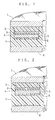
- Fig. 1 is a view partly in vertical section and showing the structure of a magneto-optic disc as an example of memory device of the invention.
- a transparent glass substrate 1.2 mm in thickness and 13 cm in diameter.
- a first transparent dielectric film 2 having a thickness of 80 nm and made of transparent aluminum nitride (AlN) is formed on the transparent substrate 1.
- a thin film (recording medium) 3 having a thickness of 20 nm and made of a rare earthtransition metal alloy of the composition (Gd x Tb 1-x ) y Fe 1-y wherein x is 0.58 to 0.62, and y is 0.27 to 0.33.
- the magneto-optic memory layer comprising these films is covered in its entirety with a layer 7 of acrylate adhesive cured with ultraviolet radiation.
- a transparent glass substrate 8 having the same size as the substrate 1 and spaced therefrom by a distance of about 30 ⁇ m is bonded to the memory layer.
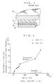
- the reliability of magneto-optic memory devices is evaluated by checking the devices for moistureproofness.
- the moistureproofness is determined usually by subjecting the device to a so-called accelerated test wherein the device is allowed to stand at a high temperature and high humidity, and observing the resulting pinholes with the unaided eye or microscopically to evaluate the moistureproofness in terms of the susceptibility of the device to pinholes.
- the term "pinhole” as used herein refers to local oxidation of the thin film forming the device to a transparent oxide, which appears like a pinhole as distinguished from the neighboring nonoxidized portion.
- the moistureproofness was evaluated by the above method.
- the accelerated test was conducted under the conditions of the so-called pressure cooker test, i.e. at 120° C/100% RH at 2 atm.
- the test samples were the following two kinds of devices.
- the samples were checked for pinholes at an interval of 2 hours after the start of testing.
- the device of the invention was at least 30 times as high as the conventional one in moistureproofness. This appears to indicate that the adhesive exhibits higher adhesion to the metal nitride film 6 than to the light reflecting film 5, inhibiting penetration of moisture or water into the memory layer.
- a magneto-optic disc of the invention was prepared which had the same construction as the device of Example 1 except that the transparent glass substrate 8 used in Example 1 was replaced by a similar substrate 8 formed with a metal nitride film 9 (5 nm in thickness) on its surface, as seen in Fig. 2.
- This disc (3) and a magneto-optic disc (4) having the same construction as the disc (3) except that the metal nitride film 6 was absent were subjected to the same pressure cooker test as in Example 1 for the evaluation of moistureproofness.
- the disc (3) was at least 10 times as high as the disc (4) in moistureproofness.
- metal is normally taken to include certain elements, sometimes called metalloids, which exhibit some of the properties of true metals, silicon being an example thereof; the term metal is so used herein.
Applications Claiming Priority (4)
| Application Number | Priority Date | Filing Date | Title |
|---|---|---|---|
| JP317759/87 | 1987-12-15 | ||
| JP62317757A JP2589332B2 (ja) | 1987-12-15 | 1987-12-15 | 磁気光学記憶素子 |
| JP317757/87 | 1987-12-15 | ||
| JP62317759A JP2589333B2 (ja) | 1987-12-15 | 1987-12-15 | 磁気光学記憶素子 |
Publications (3)
| Publication Number | Publication Date |
|---|---|
| EP0321250A2 true EP0321250A2 (fr) | 1989-06-21 |
| EP0321250A3 EP0321250A3 (en) | 1990-05-16 |
| EP0321250B1 EP0321250B1 (fr) | 1993-10-13 |
Family
ID=26569136
Family Applications (1)
| Application Number | Title | Priority Date | Filing Date |
|---|---|---|---|
| EP88311888A Expired - Lifetime EP0321250B1 (fr) | 1987-12-15 | 1988-12-15 | Dispositif de mémoire magnéto-optique |
Country Status (3)
| Country | Link |
|---|---|
| EP (1) | EP0321250B1 (fr) |
| CA (1) | CA1315983C (fr) |
| DE (1) | DE3884923T2 (fr) |
Family Cites Families (4)
| Publication number | Priority date | Publication date | Assignee | Title |
|---|---|---|---|---|
| US4414650A (en) * | 1980-06-23 | 1983-11-08 | Sharp Kabushiki Kaisha | Magneto-optic memory element |
| CA1224270A (fr) * | 1983-09-16 | 1987-07-14 | Junji Hirokane | Element-memoire magneto-optique |
| JPS6129437A (ja) * | 1984-07-20 | 1986-02-10 | Canon Inc | 光磁気記録媒体 |
| EP0239390A3 (fr) * | 1986-03-27 | 1989-04-26 | Canon Kabushiki Kaisha | Moyen d'enregistrement optomagnétique |
-
1988
- 1988-12-14 CA CA000585837A patent/CA1315983C/fr not_active Expired - Fee Related
- 1988-12-15 EP EP88311888A patent/EP0321250B1/fr not_active Expired - Lifetime
- 1988-12-15 DE DE88311888T patent/DE3884923T2/de not_active Expired - Fee Related
Also Published As
| Publication number | Publication date |
|---|---|
| DE3884923T2 (de) | 1994-05-05 |
| CA1315983C (fr) | 1993-04-13 |
| DE3884923D1 (de) | 1993-11-18 |
| EP0321250A3 (en) | 1990-05-16 |
| EP0321250B1 (fr) | 1993-10-13 |
Similar Documents
| Publication | Publication Date | Title |
|---|---|---|
| CA2017284C (fr) | Support d'enregistrement optique | |
| US4610912A (en) | Magneto-optic memory element | |
| US4579777A (en) | Opto-magnetic recording medium | |
| US4414650A (en) | Magneto-optic memory element | |
| EP0297689B1 (fr) | Elément de mémoire magnéto-optique | |
| CA1209698A (fr) | Memoire magneto-optique | |
| US5492773A (en) | Magneto-optical recording medium | |
| US4786559A (en) | Magnetooptical storage element | |
| US4711821A (en) | Opto-magnetic recording medium | |
| US5914198A (en) | Magneto-optical recording medium having dielectric layers with different indices of refraction | |
| US5305254A (en) | Magneto-optic memory device | |
| EP0321250B1 (fr) | Dispositif de mémoire magnéto-optique | |
| EP0762413A1 (fr) | Milieux magnétooptiques | |
| EP0419295B1 (fr) | Dispositif de mémorisation optique | |
| US5643650A (en) | Magneto-optical recording medium | |
| US5340647A (en) | Optomagnetic recording medium | |
| JPH06223420A (ja) | 光磁気記録媒体 | |
| US4977019A (en) | Magnetooptical recording medium bonded with a flexible foam adhesive | |
| JP2589332B2 (ja) | 磁気光学記憶素子 | |
| JP2589333B2 (ja) | 磁気光学記憶素子 | |
| JPS6369048A (ja) | 光記録媒体 | |
| JPS60219654A (ja) | 光メモリ素子 | |
| JP2882656B2 (ja) | 光ディスク | |
| JP2814601B2 (ja) | 光磁気記録媒体 | |
| JP2918628B2 (ja) | 光ディスク |
Legal Events
| Date | Code | Title | Description |
|---|---|---|---|
| PUAI | Public reference made under article 153(3) epc to a published international application that has entered the european phase |
Free format text: ORIGINAL CODE: 0009012 |
|
| AK | Designated contracting states |
Kind code of ref document: A2 Designated state(s): DE FR GB IT NL |
|
| PUAL | Search report despatched |
Free format text: ORIGINAL CODE: 0009013 |
|
| AK | Designated contracting states |
Kind code of ref document: A3 Designated state(s): DE FR GB IT NL |
|
| 17P | Request for examination filed |
Effective date: 19900711 |
|
| 17Q | First examination report despatched |
Effective date: 19920317 |
|
| GRAA | (expected) grant |
Free format text: ORIGINAL CODE: 0009210 |
|
| AK | Designated contracting states |
Kind code of ref document: B1 Designated state(s): DE FR GB IT NL |
|
| REF | Corresponds to: |
Ref document number: 3884923 Country of ref document: DE Date of ref document: 19931118 |
|
| ET | Fr: translation filed | ||
| ITF | It: translation for a ep patent filed | ||
| PLBE | No opposition filed within time limit |
Free format text: ORIGINAL CODE: 0009261 |
|
| STAA | Information on the status of an ep patent application or granted ep patent |
Free format text: STATUS: NO OPPOSITION FILED WITHIN TIME LIMIT |
|
| 26N | No opposition filed | ||
| PGFP | Annual fee paid to national office [announced via postgrant information from national office to epo] |
Ref country code: GB Payment date: 19971208 Year of fee payment: 10 |
|
| PGFP | Annual fee paid to national office [announced via postgrant information from national office to epo] |
Ref country code: FR Payment date: 19971209 Year of fee payment: 10 |
|
| PGFP | Annual fee paid to national office [announced via postgrant information from national office to epo] |
Ref country code: NL Payment date: 19971223 Year of fee payment: 10 |
|
| PG25 | Lapsed in a contracting state [announced via postgrant information from national office to epo] |
Ref country code: GB Free format text: LAPSE BECAUSE OF NON-PAYMENT OF DUE FEES Effective date: 19981215 |
|
| PG25 | Lapsed in a contracting state [announced via postgrant information from national office to epo] |
Ref country code: NL Free format text: LAPSE BECAUSE OF NON-PAYMENT OF DUE FEES Effective date: 19990701 |
|
| GBPC | Gb: european patent ceased through non-payment of renewal fee |
Effective date: 19981215 |
|
| PG25 | Lapsed in a contracting state [announced via postgrant information from national office to epo] |
Ref country code: FR Free format text: LAPSE BECAUSE OF NON-PAYMENT OF DUE FEES Effective date: 19990831 |
|
| NLV4 | Nl: lapsed or anulled due to non-payment of the annual fee |
Effective date: 19990701 |
|
| REG | Reference to a national code |
Ref country code: FR Ref legal event code: ST |
|
| PGFP | Annual fee paid to national office [announced via postgrant information from national office to epo] |
Ref country code: DE Payment date: 20041209 Year of fee payment: 17 |
|
| PG25 | Lapsed in a contracting state [announced via postgrant information from national office to epo] |
Ref country code: IT Free format text: LAPSE BECAUSE OF NON-PAYMENT OF DUE FEES;WARNING: LAPSES OF ITALIAN PATENTS WITH EFFECTIVE DATE BEFORE 2007 MAY HAVE OCCURRED AT ANY TIME BEFORE 2007. THE CORRECT EFFECTIVE DATE MAY BE DIFFERENT FROM THE ONE RECORDED. Effective date: 20051215 |
|
| PG25 | Lapsed in a contracting state [announced via postgrant information from national office to epo] |
Ref country code: DE Free format text: LAPSE BECAUSE OF NON-PAYMENT OF DUE FEES Effective date: 20060701 |