EP0321250B1 - Magneto-optisches Speichergerät - Google Patents
Magneto-optisches Speichergerät Download PDFInfo
- Publication number
- EP0321250B1 EP0321250B1 EP88311888A EP88311888A EP0321250B1 EP 0321250 B1 EP0321250 B1 EP 0321250B1 EP 88311888 A EP88311888 A EP 88311888A EP 88311888 A EP88311888 A EP 88311888A EP 0321250 B1 EP0321250 B1 EP 0321250B1
- Authority
- EP
- European Patent Office
- Prior art keywords
- film
- magneto
- memory device
- substrate
- optic memory
- Prior art date
- Legal status (The legal status is an assumption and is not a legal conclusion. Google has not performed a legal analysis and makes no representation as to the accuracy of the status listed.)
- Expired - Lifetime
Links
- 239000000758 substrate Substances 0.000 claims description 45
- 229910052751 metal Inorganic materials 0.000 claims description 30
- 239000002184 metal Substances 0.000 claims description 30
- 229910045601 alloy Inorganic materials 0.000 claims description 28
- 239000000956 alloy Substances 0.000 claims description 28
- 150000004767 nitrides Chemical class 0.000 claims description 22
- 229910052723 transition metal Inorganic materials 0.000 claims description 13
- 239000012790 adhesive layer Substances 0.000 claims description 8
- 239000011521 glass Substances 0.000 claims description 8
- 229910052782 aluminium Inorganic materials 0.000 claims description 7
- XAGFODPZIPBFFR-UHFFFAOYSA-N aluminium Chemical compound [Al] XAGFODPZIPBFFR-UHFFFAOYSA-N 0.000 claims description 6
- PIGFYZPCRLYGLF-UHFFFAOYSA-N Aluminum nitride Chemical compound [Al]#N PIGFYZPCRLYGLF-UHFFFAOYSA-N 0.000 claims description 4
- PXHVJJICTQNCMI-UHFFFAOYSA-N Nickel Chemical compound [Ni] PXHVJJICTQNCMI-UHFFFAOYSA-N 0.000 claims description 4
- 239000004411 aluminium Substances 0.000 claims description 4
- 239000003822 epoxy resin Substances 0.000 claims description 4
- 239000000203 mixture Substances 0.000 claims description 4
- 229920005668 polycarbonate resin Polymers 0.000 claims description 4
- 239000004431 polycarbonate resin Substances 0.000 claims description 4
- 229920000647 polyepoxide Polymers 0.000 claims description 4
- 239000004925 Acrylic resin Substances 0.000 claims description 3
- 229920000178 Acrylic resin Polymers 0.000 claims description 3
- 229910017083 AlN Inorganic materials 0.000 claims description 3
- 229910052581 Si3N4 Inorganic materials 0.000 claims description 3
- HQVNEWCFYHHQES-UHFFFAOYSA-N silicon nitride Chemical compound N12[Si]34N5[Si]62N3[Si]51N64 HQVNEWCFYHHQES-UHFFFAOYSA-N 0.000 claims description 3
- 239000010936 titanium Substances 0.000 claims description 3
- 229910052719 titanium Inorganic materials 0.000 claims description 3
- NPXOKRUENSOPAO-UHFFFAOYSA-N Raney nickel Chemical compound [Al].[Ni] NPXOKRUENSOPAO-UHFFFAOYSA-N 0.000 claims description 2
- BQCADISMDOOEFD-UHFFFAOYSA-N Silver Chemical compound [Ag] BQCADISMDOOEFD-UHFFFAOYSA-N 0.000 claims description 2
- 229910001069 Ti alloy Inorganic materials 0.000 claims description 2
- RTAQQCXQSZGOHL-UHFFFAOYSA-N Titanium Chemical compound [Ti] RTAQQCXQSZGOHL-UHFFFAOYSA-N 0.000 claims description 2
- UQZIWOQVLUASCR-UHFFFAOYSA-N alumane;titanium Chemical compound [AlH3].[Ti] UQZIWOQVLUASCR-UHFFFAOYSA-N 0.000 claims description 2
- 239000000919 ceramic Substances 0.000 claims description 2
- PCHJSUWPFVWCPO-UHFFFAOYSA-N gold Chemical compound [Au] PCHJSUWPFVWCPO-UHFFFAOYSA-N 0.000 claims description 2
- 229910052737 gold Inorganic materials 0.000 claims description 2
- 239000010931 gold Substances 0.000 claims description 2
- 229910044991 metal oxide Inorganic materials 0.000 claims description 2
- 150000004706 metal oxides Chemical class 0.000 claims description 2
- 229910052976 metal sulfide Inorganic materials 0.000 claims description 2
- 229910052759 nickel Inorganic materials 0.000 claims description 2
- 229910052709 silver Inorganic materials 0.000 claims description 2
- 239000004332 silver Substances 0.000 claims description 2
- 229910052715 tantalum Inorganic materials 0.000 claims description 2
- GUVRBAGPIYLISA-UHFFFAOYSA-N tantalum atom Chemical compound [Ta] GUVRBAGPIYLISA-UHFFFAOYSA-N 0.000 claims description 2
- 230000001419 dependent effect Effects 0.000 claims 2
- 229910000990 Ni alloy Inorganic materials 0.000 claims 1
- KMWBBMXGHHLDKL-UHFFFAOYSA-N [AlH3].[Si] Chemical compound [AlH3].[Si] KMWBBMXGHHLDKL-UHFFFAOYSA-N 0.000 claims 1
- 239000010408 film Substances 0.000 description 92
- 239000010410 layer Substances 0.000 description 13
- 238000012360 testing method Methods 0.000 description 11
- 239000000853 adhesive Substances 0.000 description 10
- 230000001070 adhesive effect Effects 0.000 description 10
- 239000010409 thin film Substances 0.000 description 10
- PMHQVHHXPFUNSP-UHFFFAOYSA-M copper(1+);methylsulfanylmethane;bromide Chemical compound Br[Cu].CSC PMHQVHHXPFUNSP-UHFFFAOYSA-M 0.000 description 5
- 238000000034 method Methods 0.000 description 5
- 230000003647 oxidation Effects 0.000 description 5
- 238000007254 oxidation reaction Methods 0.000 description 5
- 238000010276 construction Methods 0.000 description 4
- 238000005260 corrosion Methods 0.000 description 4
- 230000007797 corrosion Effects 0.000 description 4
- 238000004544 sputter deposition Methods 0.000 description 4
- PNEYBMLMFCGWSK-UHFFFAOYSA-N Alumina Chemical compound [O-2].[O-2].[O-2].[Al+3].[Al+3] PNEYBMLMFCGWSK-UHFFFAOYSA-N 0.000 description 3
- 230000005374 Kerr effect Effects 0.000 description 3
- 230000000694 effects Effects 0.000 description 3
- 238000002474 experimental method Methods 0.000 description 3
- 150000002739 metals Chemical class 0.000 description 3
- 238000011160 research Methods 0.000 description 3
- 125000004429 atom Chemical group 0.000 description 2
- 230000015556 catabolic process Effects 0.000 description 2
- 230000000052 comparative effect Effects 0.000 description 2
- 238000006731 degradation reaction Methods 0.000 description 2
- 230000007774 longterm Effects 0.000 description 2
- 230000005855 radiation Effects 0.000 description 2
- 239000000126 substance Substances 0.000 description 2
- NIXOWILDQLNWCW-UHFFFAOYSA-M Acrylate Chemical compound [O-]C(=O)C=C NIXOWILDQLNWCW-UHFFFAOYSA-M 0.000 description 1
- 229910000838 Al alloy Inorganic materials 0.000 description 1
- 229920003319 Araldite® Polymers 0.000 description 1
- OKTJSMMVPCPJKN-UHFFFAOYSA-N Carbon Chemical compound [C] OKTJSMMVPCPJKN-UHFFFAOYSA-N 0.000 description 1
- 239000004831 Hot glue Substances 0.000 description 1
- VYPSYNLAJGMNEJ-UHFFFAOYSA-N Silicium dioxide Chemical compound O=[Si]=O VYPSYNLAJGMNEJ-UHFFFAOYSA-N 0.000 description 1
- 239000004830 Super Glue Substances 0.000 description 1
- 239000005083 Zinc sulfide Substances 0.000 description 1
- NIXOWILDQLNWCW-UHFFFAOYSA-N acrylic acid group Chemical group C(C=C)(=O)O NIXOWILDQLNWCW-UHFFFAOYSA-N 0.000 description 1
- 239000003522 acrylic cement Substances 0.000 description 1
- CSDREXVUYHZDNP-UHFFFAOYSA-N alumanylidynesilicon Chemical compound [Al].[Si] CSDREXVUYHZDNP-UHFFFAOYSA-N 0.000 description 1
- QVGXLLKOCUKJST-UHFFFAOYSA-N atomic oxygen Chemical compound [O] QVGXLLKOCUKJST-UHFFFAOYSA-N 0.000 description 1
- 229910052799 carbon Inorganic materials 0.000 description 1
- 229910052804 chromium Inorganic materials 0.000 description 1
- 230000003247 decreasing effect Effects 0.000 description 1
- 238000011161 development Methods 0.000 description 1
- 229920006332 epoxy adhesive Polymers 0.000 description 1
- 238000011156 evaluation Methods 0.000 description 1
- -1 for example Chemical class 0.000 description 1
- 229920000159 gelatin Polymers 0.000 description 1
- 238000010438 heat treatment Methods 0.000 description 1
- 125000005842 heteroatom Chemical group 0.000 description 1
- 230000001771 impaired effect Effects 0.000 description 1
- 230000002401 inhibitory effect Effects 0.000 description 1
- 229910052752 metalloid Inorganic materials 0.000 description 1
- 150000002738 metalloids Chemical class 0.000 description 1
- 230000003287 optical effect Effects 0.000 description 1
- 229910052760 oxygen Inorganic materials 0.000 description 1
- 239000001301 oxygen Substances 0.000 description 1
- 230000035515 penetration Effects 0.000 description 1
- 239000004033 plastic Substances 0.000 description 1
- 229920003023 plastic Polymers 0.000 description 1
- 230000000750 progressive effect Effects 0.000 description 1
- 230000002035 prolonged effect Effects 0.000 description 1
- 238000007789 sealing Methods 0.000 description 1
- 229910052710 silicon Inorganic materials 0.000 description 1
- 239000010703 silicon Substances 0.000 description 1
- 229910052814 silicon oxide Inorganic materials 0.000 description 1
- 229910001220 stainless steel Inorganic materials 0.000 description 1
- 239000010935 stainless steel Substances 0.000 description 1
- XLYOFNOQVPJJNP-UHFFFAOYSA-N water Substances O XLYOFNOQVPJJNP-UHFFFAOYSA-N 0.000 description 1
- 229910052727 yttrium Inorganic materials 0.000 description 1
- VWQVUPCCIRVNHF-UHFFFAOYSA-N yttrium atom Chemical compound [Y] VWQVUPCCIRVNHF-UHFFFAOYSA-N 0.000 description 1
- 229910052984 zinc sulfide Inorganic materials 0.000 description 1
- DRDVZXDWVBGGMH-UHFFFAOYSA-N zinc;sulfide Chemical compound [S-2].[Zn+2] DRDVZXDWVBGGMH-UHFFFAOYSA-N 0.000 description 1
Images

Classifications
-
- G—PHYSICS
- G11—INFORMATION STORAGE
- G11B—INFORMATION STORAGE BASED ON RELATIVE MOVEMENT BETWEEN RECORD CARRIER AND TRANSDUCER
- G11B11/00—Recording on or reproducing from the same record carrier wherein for these two operations the methods are covered by different main groups of groups G11B3/00 - G11B7/00 or by different subgroups of group G11B9/00; Record carriers therefor
- G11B11/10—Recording on or reproducing from the same record carrier wherein for these two operations the methods are covered by different main groups of groups G11B3/00 - G11B7/00 or by different subgroups of group G11B9/00; Record carriers therefor using recording by magnetic means or other means for magnetisation or demagnetisation of a record carrier, e.g. light induced spin magnetisation; Demagnetisation by thermal or stress means in the presence or not of an orienting magnetic field
- G11B11/105—Recording on or reproducing from the same record carrier wherein for these two operations the methods are covered by different main groups of groups G11B3/00 - G11B7/00 or by different subgroups of group G11B9/00; Record carriers therefor using recording by magnetic means or other means for magnetisation or demagnetisation of a record carrier, e.g. light induced spin magnetisation; Demagnetisation by thermal or stress means in the presence or not of an orienting magnetic field using a beam of light or a magnetic field for recording by change of magnetisation and a beam of light for reproducing, i.e. magneto-optical, e.g. light-induced thermomagnetic recording, spin magnetisation recording, Kerr or Faraday effect reproducing
- G11B11/10582—Record carriers characterised by the selection of the material or by the structure or form
- G11B11/10586—Record carriers characterised by the selection of the material or by the structure or form characterised by the selection of the material
- G11B11/10589—Details
- G11B11/10593—Details for improving read-out properties, e.g. polarisation of light
-
- G—PHYSICS
- G11—INFORMATION STORAGE
- G11B—INFORMATION STORAGE BASED ON RELATIVE MOVEMENT BETWEEN RECORD CARRIER AND TRANSDUCER
- G11B11/00—Recording on or reproducing from the same record carrier wherein for these two operations the methods are covered by different main groups of groups G11B3/00 - G11B7/00 or by different subgroups of group G11B9/00; Record carriers therefor
- G11B11/10—Recording on or reproducing from the same record carrier wherein for these two operations the methods are covered by different main groups of groups G11B3/00 - G11B7/00 or by different subgroups of group G11B9/00; Record carriers therefor using recording by magnetic means or other means for magnetisation or demagnetisation of a record carrier, e.g. light induced spin magnetisation; Demagnetisation by thermal or stress means in the presence or not of an orienting magnetic field
- G11B11/105—Recording on or reproducing from the same record carrier wherein for these two operations the methods are covered by different main groups of groups G11B3/00 - G11B7/00 or by different subgroups of group G11B9/00; Record carriers therefor using recording by magnetic means or other means for magnetisation or demagnetisation of a record carrier, e.g. light induced spin magnetisation; Demagnetisation by thermal or stress means in the presence or not of an orienting magnetic field using a beam of light or a magnetic field for recording by change of magnetisation and a beam of light for reproducing, i.e. magneto-optical, e.g. light-induced thermomagnetic recording, spin magnetisation recording, Kerr or Faraday effect reproducing
- G11B11/10582—Record carriers characterised by the selection of the material or by the structure or form
Definitions
- the present invention relates to magneto-optic memory devices, and more particularly to magneto-optic memory devices, such as magneto-optic discs and magneto-optic cards, which are adapted to record data thereon and reproduce or erase the data therefrom when exposed, for example, to a laser beam.
- magneto-optic memory devices as optical memory devices adapted for recording, reproducing and erasing data.
- a rare earth-transition metal alloy thin film is used as the memory medium because the recording bits are free of the influence of the grain boundary and further because the film serving as the memory medium can be formed over a large area relatively easily.
- the magneto-optic memory devices incorporating the rare earth-transition metal alloy thin film as the memory medium generally fail to exhibit satisfactory magneto optic effects (Kerr effect and Faraday effect) and therefore still remain to be improved in the S/N ratio of reproduction signals.
- the so-called reflective film structure is employed for magneto-optic memory devices as already disclosed, for example, in Unexamined Japanese Patent Publication SHO 57-12428 and Applied Optics, Vol. 23, No. 22, p. 3972.
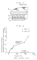
- Fig. 3 is a view partly in vertical section and showing a conventional magneto-optic memory device of reflective film structure.
- indicated at a is a transparent substrate of glass, polycarbonate resin, epoxy resin or the like, at b a transparent dielectric film having a higher refractive index than the substrate a , at c a rare earth-transition metal alloy thin film, at d a transparent dielectric film, and at e a light reflecting film of metal.
- the rare earth-transition metal alloy film c is so thin that the light incident on the film c partly passes through the film. Consequently, reproduction light exhibits the Kerr effect due to the reflection at the surface of the film c and, in combination therewith, the Faraday effect which is produced by the portion of the light passing through the film c , reflected at the reflecting film e and passing through the film c again. This results in a Kerr rotation angle which is apparently several times as great as the angle afforded by the Kerr effect only.
- the device exhibits an increased apparent Kerr rotation angle of 1.6 degrees (although a single GdTbFe film is about 0.3 degree in this angle) when the device comprises a glass substrate as the transparent substrate a , AlN film as the transparent dielectric film b , GdTbFe fi)m as the rare earth-transition metal alloy film c , AlN film as the transparent dielectric film d and Al film as the light reflecting film e .
- the rare earth-transition metal alloy thin film is very susceptible to oxidation in the presence of moisture and loses the inherent magneto-optic characteristics thereof on oxidation.
- the film is more prone to the influence of oxidation because the film must have a considerably decreased thickness and also because the film is left exposed at its end. In other words, the device has the problem of being poor in long term reliability.
- the device of reflective film structure described above is used usually with another substrate laminated to the reflecting film with an adhesive layer.
- the adhesive layer is used for covering the entire magneto-optic memory layer comprising the dielectric film b , alloy film c , dielectric film d and light reflecting film e and also for adhering the other substrate.
- the magneto-optic memory layer including the alloy film will be held out of direct contact with the atmosphere, with the alloy film protected against oxidation, so as to assure the device of reliability.
- the object of the present invention is to overcome the foregoing problem and to provide a magneto-optic memory device of reflective film structure which exhibits outstanding magneto-optic characteristics over a prolonged period of time.
- the present invention provides a magneto-optic memory device comprising a first, transparent substrate on which is mounted a magneto-optic memory film of rare earth-transition metal alloy with a reflecting film disposed to the side of said memory film remote from said first substrate; and a second substrate bonded by an adhesive layer to the first substrate with said memory and reflecting films disposed therebetween, characterised by the provision of a film comprising a metal nitride between the reflecting film and the adhesive layer.
- the magneto-optic memory device of the present invention is remarkably improved in moistureproofness and consequently greatly improved in reliability without impairing the inherent magneto-optic characteristics thereof.
- the second substrate opposed to the first (transparent) substrate may be formed with the same metal nitride film as above over the surface thereof opposed to the transparent substrate.
- the use of this metal nitride film on the second substrate further improves the memory device in moistureproofness and reliability.
- a pair of substrates are used, at least one (the first) of which is a transparent substrate.
- the transparent substrate can be prepared from glass, polycarbonate resin, acrylic resin, epoxy resin or like plastics.
- the other (second) substrate which may be a similar transparent substrate, can be a nontransparent substrate, for example, of aluminium or ceramics.
- Examples of useful dielectric films for forming a magneto-optic memory layer with the memory film are transparent metal nitride film, metal oxide films, metal sulfide films and the like, such as silicon nitride, aluminium nitride, silicon oxide, aluminium oxide and zinc sulfide films.
- the dielectric film may be doped with a hetero element such as yttrium, oxygen, carbon or the like and thereby given a higher dielectric constant.
- the dielectric film can be formed by a known process such as CVD, sputtering or the like.
- a first dielectric film is formed on the transparent substrate and a second on a rare earth-transition metal alloy thin film.
- the dielectric film on the transparent substrate has a thickness of 50 to 100 nm, and the one on the alloy thin film is 10 to 100 nm in thickness.
- the rare earth-transition metal alloy thin memory film can be made of an alloy used in the art, such as GdTbFeCo, TbFeCo, TbCo, TbFe or like alloy. However, it is desirable to use a thin film of a rare earth-transition metal alloy or the composition: (Gd x Tb 1-x ) y Fe 1-y wherein most preferably, x is 0.58 to 0.62, and y is 0.27 to 0.33. Use of the alloy of the composition wherein x and y are in these ranges affords magneto-optic memory devices giving data reproduction signals of a high quality, especially a high C/N ratio (carrier to noise ratio) in excess of 50 dB.
- Such an alloy film can be formed on the dielectric film by CVD, sputtering or the like known process. It is suitable that the film be 5 nm to 100 nm in thickness. To inhibit the possible corrosion due to moisture, the alloy film may be doped with a small quantity of corrosion-resistant metal atoms such as Cr, Ti, Al, Ta, Ni or like atoms.
- the light reflecting film is a metal film capable of reflecting light efficiently and having high corrosion resistance.
- metals useful for the reflecting film are aluminium, nickel, titanium, gold, silver, tantalum, stainless steel and the like. Also usable are alloys of such metals including, for example, aluminum-nickel alloy and aluminum-titanium alloy. It is especially desirable to use aluminum or aluminum alloy.
- the reflecting film can be formed by a known process such as CVD or sputtering and is suitably 10 to 300 nm in thickness.
- the magneto-optic memory layer composed of the films described above is formed usually on a portion of the transparent substrate.
- the adhesive for covering the memory layer and bonding the other substrate can be one of various adhesives known in the art and including those curable at room temperature, by heating or with ultraviolet radiation or electron rays. Of these, it is suitable to use one having high moisture resistance. More specific examples of such adhesives are cyano-acrylate adhesives [Aron Alpha (Toagosei Chemical Industry Co., Ltd., Japan), Cyanobond (Sumitomo Chemical Co., Ltd., Japan)], ultaviolet-curable adhesives [Three Bond 3000 series (Three Bond Co., Ltd., Japan), Photobond (Meisei Churchill Co., Ltd., Japan)], aerophobic adhesives [Loctite (Japan Loctite Co., Ltd., Japan), Three Bond 1300 series], epoxy adhesives [Araldite (CIBA), Sumikadine (Sumitomo Chemical Co., Ltd.), Cemedine (Cemedine Co., Ltd., Japan)], two-com
- a metal nitride film is formed on the magneto-optic memory layer, i.e. on the light reflecting film, before the other substrate is bonded to the memory layer with the adhesive.
- suitable metal nitride films are silicon nitride, aluminum nitride, silicon-aluminum nitride films and the like, among which aluminum nitride film is preferable to use.
- the metal nitride film can be formed by CVD, sputtering or like process. The thickness of this film is suitably 5 to 1000 nm, more suitably 10 to 500 nm.
- the other substrate is bonded to the film by applying and curing the adhesive, whereby a magneto-optic memory device of the invention can be obtained.
- the other substrate is preferably one formed with the same metal nitride film as above on the surface thereof opposed to the transparent substrate.
- the nitride film be formed at least over the area opposed to and covering the memory layer.
- the configuration of the memory device thus obtained is not limited specifically.
- the device is in the form of a disk (magneto-optic disc) or rectangular (magneto-optic card).
- Fig. 1 is a view partly in vertical section and showing the structure of a magneto-optic disc as an example of memory device of the invention.
- a transparent glass substrate 1.2 mm in thickness and 13 cm in diameter.
- a first transparent dielectric film 2 having a thickness of 80 nm and made of transparent aluminum nitride (AlN) is formed on the transparent substrate 1.
- a thin film (recording medium) 3 having a thickness of 20 nm and made of a rare earth-transition metal alloy of the composition (Gd x Tb 1-x ) y Fe 1-y wherein x is 0.58 to 0.62, and y is 0.27 to 0.33.
- the magneto-optic memory layer comprising these films is covered in its entirety with a layer 7 of acrylate adhesive cured with ultraviolet radiation.
- a transparent glass substrate 8 having the same size as the substrate 1 and spaced therefrom by a distance of about 30 ⁇ m is bonded to the memory layer.
- the reliability of magneto-optic memory devices is evaluated by checking the devices for moistureproofness.
- the moistureproofness is determined usually by subjecting the device to a so-called accelerated test wherein the device is allowed to stand at a high temperature and high humidity, and observing the resulting pinholes with the unaided eye or microscopically to evaluate the moistureproofness in terms of the susceptibility of the device to pinholes.
- the term "pinhole” as used herein refers to local oxidation of the thin film forming the device to a transparent oxide, which appears like a pinhole as distinguished from the neighboring nonoxidized portion.
- the moistureproofness was evaluated by the above method.
- the accelerated test was conducted under the conditions of the so-called pressure cooker test, i.e. at 120° C/100% RH at 2 atm.
- the test samples were the following two kinds of devices.
- the samples were checked for pinholes at an interval of 2 hours after the start of testing.
- the device of the invention was at least 30 times as high as the conventional one in moistureproofness. This appears to indicate that the adhesive exhibits higher adhesion to the metal nitride film 6 than to the light reflecting film 5, inhibiting penetration of moisture or water into the memory layer.
- a magneto-optic disc of the invention was prepared which had the same construction as the device of Example 1 except that the transparent glass substrate 8 used in Example 1 was replaced by a similar substrate 8 formed with a metal nitride film 9 (5 nm in thickness) on its surface, as seen in Fig. 2.
- This disc (3) and a magneto-optic disc (4) having the same construction as the disc (3) except that the metal nitride film 6 was absent were subjected to the same pressure cooker test as in Example 1 for the evaluation of moistureproofness.
- the disc (3) was at least 10 times as high as the disc (4) in moistureproofness.
- metal is normally taken to include certain elements, sometimes called metalloids, which exhibit some of the properties of true metals, silicon being an example thereof; the term metal is so used herein.
Claims (17)
- Magneto-optische Speichereinrichtung mit einem ersten, lichtdurchlässigen Substrat (1), auf dem ein magneto-optischer Speicherfilm (3) aus einer Seltenerd/Übergangsmetall-Legierung aufgebracht ist, wobei ein Reflexionsfilm (5) auf der dem ersten Substrat (1) abgewandten Seite dieses Speicherfilms angeordnet ist; und einem zweiten Substrat (8), das durch eine Kleberschicht (5) mit dem ersten Substrat verbunden ist, wobei der Speicher- und der Reflexionsfilm dazwischenliegen, gekennzeichnet durch einen Film (6) mit einem Metallnitrid zwischen dem Reflexionsfilm (5) und der Kleberschicht (7).
- Magneto-optische Speichereinrichtung nach Anspruch 1, die ferner folgendes aufweist:- einen ersten dielektrischen Film (2), der zwischen dem ersten Substrat und dem Speicherfilm angeordnet ist, und einen zweiten dielektrischen Film (4), der zwischen dem Speicherfilm und dem Reflexionsfilm angeordnet ist.
- Magneto-optische Speichereinrichtung nach Anspruch 1 oder Anspruch 2, bei der der Metallnitridfilm (6) aus Siliziumnitrid, Aluminiumnitrid oder Silizium-Aluminium-Nitrid besteht.
- Magneto-optische Speichereinrichtung nach einem der vorstehenden Ansprüche, bei der der Metallnitridfilm eine Dicke von 5 bis 1.000 nm aufweist.
- Magneto-optische Speichereinrichtung nach Anspruch 4, bei der der Metallnitridfilm eine Dicke von 10 bis 500 nm aufweist.
- Magneto-optische Speichereinrichtung nach einem der vorstehenden Ansprüche, bei der der Speicherfilm aus einer GdTbFe-, GdTbFeCo-, TbFeCo-, TbCo- oder TbFe-Legierung besteht.
- Magneto-optische Speichereinrichtung nach Anspruch 6, bei der der Speicherfilm aus einer GdTbFe-Legierung besteht.
- Magneto-optische Speichereinrichtung nach Anspruch 7, bei der die GdTbFe-Legierung die folgende Verbindungsformel aufweist:
(GdxTb1-x)yFe1-y
wobei x 0,58 bis 0,62 und y 0,27 bis 0,33 sind. - Magneto-optische Speichereinrichtung nach einem der vorstehenden Ansprüche, bei der der Speicherfilm eine Dicke von 5 bis 100 nm aufweist.
- Magneto-optische Speichereinrichtung nach Anspruch 2 oder einem von diesem abhängigen Anspruch, bei der der erste und der zweite dielektrische Film jeweils aus einem Metallnitrid, einem Metalloxid oder einem Metallsulfid bestehen.
- Magneto-optische Speichereinrichtung nach Anspruch 2 oder nach einem von diesem abhängigen Anspruch, bei der der erste dielektrische Film eine Dicke von 50 bis 100 nm und der zweite dielektrische Film eine Dicke von 10 bis 100 nm aufweisen.
- Magneto-optische Speichereinrichtung nach einem der vorstehenden Ansprüche, bei der der Lichtreflexionsfilm aus Aluminium, Nickel, Titan, Gold, Silber, Tantal, einer Aluminium-Nickel-Legierung oder einer Aluminium-Titan-Legierung besteht.
- Magneto-optische Speichereinrichtung nach einem der vorstehenden Ansprüche, bei der der Lichtreflexionsfilm eine Dicke von 10 bis 300 nm aufweist.
- Magneto-optische Speichereinrichtung nach einem der vorstehenden Ansprüche, bei der das erste Substrat ein Glas-, Polycarbonatharz-, Acrylharz- oder Epoxidharzsubstrat ist.
- Magneto-optische Speichereinrichtung nach einem der vorstehenden Ansprüche, bei der das zweite Substrat ein Glas-, Polycarbonatharz-, Acrylharz-, Epoxidharz-, Aluminium- oder Keramiksubstrat ist.
- Magneto-optische Speichereinrichtung nach einem der vorstehenden Ansprüche, bei der das zweite Substrat auf seiner dem ersten Substrat gegenüberliegenden Oberfläche einen Metallnitridfilm (9) aufweist.
- Einrichtung nach Anspruch 1, die in Form einer Platte oder eines Rechtecks vorliegt.
Applications Claiming Priority (4)
| Application Number | Priority Date | Filing Date | Title |
|---|---|---|---|
| JP317759/87 | 1987-12-15 | ||
| JP62317757A JP2589332B2 (ja) | 1987-12-15 | 1987-12-15 | 磁気光学記憶素子 |
| JP317757/87 | 1987-12-15 | ||
| JP62317759A JP2589333B2 (ja) | 1987-12-15 | 1987-12-15 | 磁気光学記憶素子 |
Publications (3)
| Publication Number | Publication Date |
|---|---|
| EP0321250A2 EP0321250A2 (de) | 1989-06-21 |
| EP0321250A3 EP0321250A3 (en) | 1990-05-16 |
| EP0321250B1 true EP0321250B1 (de) | 1993-10-13 |
Family
ID=26569136
Family Applications (1)
| Application Number | Title | Priority Date | Filing Date |
|---|---|---|---|
| EP88311888A Expired - Lifetime EP0321250B1 (de) | 1987-12-15 | 1988-12-15 | Magneto-optisches Speichergerät |
Country Status (3)
| Country | Link |
|---|---|
| EP (1) | EP0321250B1 (de) |
| CA (1) | CA1315983C (de) |
| DE (1) | DE3884923T2 (de) |
Family Cites Families (4)
| Publication number | Priority date | Publication date | Assignee | Title |
|---|---|---|---|---|
| US4414650A (en) * | 1980-06-23 | 1983-11-08 | Sharp Kabushiki Kaisha | Magneto-optic memory element |
| CA1224270A (en) * | 1983-09-16 | 1987-07-14 | Junji Hirokane | Magneto-optic memory element |
| JPS6129437A (ja) * | 1984-07-20 | 1986-02-10 | Canon Inc | 光磁気記録媒体 |
| EP0239390A3 (de) * | 1986-03-27 | 1989-04-26 | Canon Kabushiki Kaisha | Optisch-magnetisches Aufzeichnungsmedium |
-
1988
- 1988-12-14 CA CA000585837A patent/CA1315983C/en not_active Expired - Fee Related
- 1988-12-15 EP EP88311888A patent/EP0321250B1/de not_active Expired - Lifetime
- 1988-12-15 DE DE88311888T patent/DE3884923T2/de not_active Expired - Fee Related
Also Published As
| Publication number | Publication date |
|---|---|
| DE3884923T2 (de) | 1994-05-05 |
| CA1315983C (en) | 1993-04-13 |
| DE3884923D1 (de) | 1993-11-18 |
| EP0321250A2 (de) | 1989-06-21 |
| EP0321250A3 (en) | 1990-05-16 |
Similar Documents
| Publication | Publication Date | Title |
|---|---|---|
| CA2017284C (en) | Optical recording medium | |
| US4579777A (en) | Opto-magnetic recording medium | |
| US4610912A (en) | Magneto-optic memory element | |
| EP0297689B1 (de) | Magneto-optisches Speicherelement | |
| US4658388A (en) | Optical recording medium which includes a corrosion resistant film of a mixture of a carbide and a nitride | |
| US4786559A (en) | Magnetooptical storage element | |
| US4695510A (en) | Opto-magnetic recording medium | |
| US4711821A (en) | Opto-magnetic recording medium | |
| US5914198A (en) | Magneto-optical recording medium having dielectric layers with different indices of refraction | |
| EP0239390A2 (de) | Optisch-magnetisches Aufzeichnungsmedium | |
| EP0762413A1 (de) | Magnetooptische Medien | |
| EP0321250B1 (de) | Magneto-optisches Speichergerät | |
| US5305254A (en) | Magneto-optic memory device | |
| EP0419295B1 (de) | Optischer Speicher | |
| US5643650A (en) | Magneto-optical recording medium | |
| US5340647A (en) | Optomagnetic recording medium | |
| EP0233062A2 (de) | Magnetisch-optisches Gedächtnismedium | |
| JPH06223420A (ja) | 光磁気記録媒体 | |
| US4977019A (en) | Magnetooptical recording medium bonded with a flexible foam adhesive | |
| JP2589332B2 (ja) | 磁気光学記憶素子 | |
| JP2589333B2 (ja) | 磁気光学記憶素子 | |
| JPS6369048A (ja) | 光記録媒体 | |
| JP2882656B2 (ja) | 光ディスク | |
| JP2814601B2 (ja) | 光磁気記録媒体 | |
| JPS60219654A (ja) | 光メモリ素子 |
Legal Events
| Date | Code | Title | Description |
|---|---|---|---|
| PUAI | Public reference made under article 153(3) epc to a published international application that has entered the european phase |
Free format text: ORIGINAL CODE: 0009012 |
|
| AK | Designated contracting states |
Kind code of ref document: A2 Designated state(s): DE FR GB IT NL |
|
| PUAL | Search report despatched |
Free format text: ORIGINAL CODE: 0009013 |
|
| AK | Designated contracting states |
Kind code of ref document: A3 Designated state(s): DE FR GB IT NL |
|
| 17P | Request for examination filed |
Effective date: 19900711 |
|
| 17Q | First examination report despatched |
Effective date: 19920317 |
|
| GRAA | (expected) grant |
Free format text: ORIGINAL CODE: 0009210 |
|
| AK | Designated contracting states |
Kind code of ref document: B1 Designated state(s): DE FR GB IT NL |
|
| REF | Corresponds to: |
Ref document number: 3884923 Country of ref document: DE Date of ref document: 19931118 |
|
| ET | Fr: translation filed | ||
| ITF | It: translation for a ep patent filed | ||
| PLBE | No opposition filed within time limit |
Free format text: ORIGINAL CODE: 0009261 |
|
| STAA | Information on the status of an ep patent application or granted ep patent |
Free format text: STATUS: NO OPPOSITION FILED WITHIN TIME LIMIT |
|
| 26N | No opposition filed | ||
| PGFP | Annual fee paid to national office [announced via postgrant information from national office to epo] |
Ref country code: GB Payment date: 19971208 Year of fee payment: 10 |
|
| PGFP | Annual fee paid to national office [announced via postgrant information from national office to epo] |
Ref country code: FR Payment date: 19971209 Year of fee payment: 10 |
|
| PGFP | Annual fee paid to national office [announced via postgrant information from national office to epo] |
Ref country code: NL Payment date: 19971223 Year of fee payment: 10 |
|
| PG25 | Lapsed in a contracting state [announced via postgrant information from national office to epo] |
Ref country code: GB Free format text: LAPSE BECAUSE OF NON-PAYMENT OF DUE FEES Effective date: 19981215 |
|
| PG25 | Lapsed in a contracting state [announced via postgrant information from national office to epo] |
Ref country code: NL Free format text: LAPSE BECAUSE OF NON-PAYMENT OF DUE FEES Effective date: 19990701 |
|
| GBPC | Gb: european patent ceased through non-payment of renewal fee |
Effective date: 19981215 |
|
| PG25 | Lapsed in a contracting state [announced via postgrant information from national office to epo] |
Ref country code: FR Free format text: LAPSE BECAUSE OF NON-PAYMENT OF DUE FEES Effective date: 19990831 |
|
| NLV4 | Nl: lapsed or anulled due to non-payment of the annual fee |
Effective date: 19990701 |
|
| REG | Reference to a national code |
Ref country code: FR Ref legal event code: ST |
|
| PGFP | Annual fee paid to national office [announced via postgrant information from national office to epo] |
Ref country code: DE Payment date: 20041209 Year of fee payment: 17 |
|
| PG25 | Lapsed in a contracting state [announced via postgrant information from national office to epo] |
Ref country code: IT Free format text: LAPSE BECAUSE OF NON-PAYMENT OF DUE FEES;WARNING: LAPSES OF ITALIAN PATENTS WITH EFFECTIVE DATE BEFORE 2007 MAY HAVE OCCURRED AT ANY TIME BEFORE 2007. THE CORRECT EFFECTIVE DATE MAY BE DIFFERENT FROM THE ONE RECORDED. Effective date: 20051215 |
|
| PG25 | Lapsed in a contracting state [announced via postgrant information from national office to epo] |
Ref country code: DE Free format text: LAPSE BECAUSE OF NON-PAYMENT OF DUE FEES Effective date: 20060701 |