EP0321255B1 - Kondensatortantaloberfläche zur Verwendung als Gegenelektrodenanordnung und Verfahren - Google Patents
Kondensatortantaloberfläche zur Verwendung als Gegenelektrodenanordnung und Verfahren Download PDFInfo
- Publication number
- EP0321255B1 EP0321255B1 EP19880311896 EP88311896A EP0321255B1 EP 0321255 B1 EP0321255 B1 EP 0321255B1 EP 19880311896 EP19880311896 EP 19880311896 EP 88311896 A EP88311896 A EP 88311896A EP 0321255 B1 EP0321255 B1 EP 0321255B1
- Authority
- EP
- European Patent Office
- Prior art keywords
- tantalum
- layer
- family metal
- platinum family
- counterelectrode
- Prior art date
- Legal status (The legal status is an assumption and is not a legal conclusion. Google has not performed a legal analysis and makes no representation as to the accuracy of the status listed.)
- Expired - Lifetime
Links
- GUVRBAGPIYLISA-UHFFFAOYSA-N tantalum atom Chemical compound [Ta] GUVRBAGPIYLISA-UHFFFAOYSA-N 0.000 title claims description 97
- 229910052715 tantalum Inorganic materials 0.000 title claims description 92
- 238000000034 method Methods 0.000 title claims description 45
- 239000003990 capacitor Substances 0.000 title claims description 30
- BASFCYQUMIYNBI-UHFFFAOYSA-N platinum Chemical compound [Pt] BASFCYQUMIYNBI-UHFFFAOYSA-N 0.000 claims description 67
- 229910045601 alloy Inorganic materials 0.000 claims description 29
- 239000000956 alloy Substances 0.000 claims description 29
- 229910052751 metal Inorganic materials 0.000 claims description 26
- 239000002184 metal Substances 0.000 claims description 26
- 229910052697 platinum Inorganic materials 0.000 claims description 26
- 238000005275 alloying Methods 0.000 claims description 18
- 238000000151 deposition Methods 0.000 claims description 15
- 238000004544 sputter deposition Methods 0.000 claims description 10
- 238000005253 cladding Methods 0.000 claims description 8
- KRHYYFGTRYWZRS-UHFFFAOYSA-N Fluorane Chemical compound F KRHYYFGTRYWZRS-UHFFFAOYSA-N 0.000 claims description 4
- 238000007772 electroless plating Methods 0.000 claims description 4
- 239000002253 acid Substances 0.000 claims 2
- 239000010410 layer Substances 0.000 description 52
- 230000008021 deposition Effects 0.000 description 13
- 239000000463 material Substances 0.000 description 8
- 239000003792 electrolyte Substances 0.000 description 5
- 238000010438 heat treatment Methods 0.000 description 5
- KDLHZDBZIXYQEI-UHFFFAOYSA-N palladium Substances [Pd] KDLHZDBZIXYQEI-UHFFFAOYSA-N 0.000 description 5
- RYGMFSIKBFXOCR-UHFFFAOYSA-N Copper Chemical compound [Cu] RYGMFSIKBFXOCR-UHFFFAOYSA-N 0.000 description 4
- 229910000990 Ni alloy Inorganic materials 0.000 description 4
- PXHVJJICTQNCMI-UHFFFAOYSA-N Nickel Chemical compound [Ni] PXHVJJICTQNCMI-UHFFFAOYSA-N 0.000 description 4
- 239000010949 copper Substances 0.000 description 4
- OKTJSMMVPCPJKN-UHFFFAOYSA-N Carbon Chemical compound [C] OKTJSMMVPCPJKN-UHFFFAOYSA-N 0.000 description 3
- 230000001464 adherent effect Effects 0.000 description 3
- 229910052802 copper Inorganic materials 0.000 description 3
- 150000002739 metals Chemical class 0.000 description 3
- 229910052763 palladium Inorganic materials 0.000 description 3
- BQCADISMDOOEFD-UHFFFAOYSA-N Silver Chemical compound [Ag] BQCADISMDOOEFD-UHFFFAOYSA-N 0.000 description 2
- 229910001362 Ta alloys Inorganic materials 0.000 description 2
- 239000012190 activator Substances 0.000 description 2
- 230000015572 biosynthetic process Effects 0.000 description 2
- 239000003795 chemical substances by application Substances 0.000 description 2
- 230000002999 depolarising effect Effects 0.000 description 2
- 238000004070 electrodeposition Methods 0.000 description 2
- 229910002804 graphite Inorganic materials 0.000 description 2
- 239000010439 graphite Substances 0.000 description 2
- 229910052741 iridium Inorganic materials 0.000 description 2
- 238000003475 lamination Methods 0.000 description 2
- NFFIWVVINABMKP-UHFFFAOYSA-N methylidynetantalum Chemical compound [Ta]#C NFFIWVVINABMKP-UHFFFAOYSA-N 0.000 description 2
- 229910052759 nickel Inorganic materials 0.000 description 2
- 229910052762 osmium Inorganic materials 0.000 description 2
- 230000001590 oxidative effect Effects 0.000 description 2
- 229910052703 rhodium Inorganic materials 0.000 description 2
- 239000010948 rhodium Substances 0.000 description 2
- 229910052709 silver Inorganic materials 0.000 description 2
- 239000004332 silver Substances 0.000 description 2
- 125000006850 spacer group Chemical group 0.000 description 2
- 239000002344 surface layer Substances 0.000 description 2
- 229910003468 tantalcarbide Inorganic materials 0.000 description 2
- 229910000881 Cu alloy Inorganic materials 0.000 description 1
- LDQWGYPZNIJQIK-UHFFFAOYSA-N [Ta].[Pt] Chemical group [Ta].[Pt] LDQWGYPZNIJQIK-UHFFFAOYSA-N 0.000 description 1
- 230000004913 activation Effects 0.000 description 1
- 229910052799 carbon Inorganic materials 0.000 description 1
- 239000003638 chemical reducing agent Substances 0.000 description 1
- 238000005097 cold rolling Methods 0.000 description 1
- 238000001246 colloidal dispersion Methods 0.000 description 1
- 238000010276 construction Methods 0.000 description 1
- 230000005611 electricity Effects 0.000 description 1
- 238000002848 electrochemical method Methods 0.000 description 1
- 239000002360 explosive Substances 0.000 description 1
- 239000011888 foil Substances 0.000 description 1
- 238000005098 hot rolling Methods 0.000 description 1
- GKOZUEZYRPOHIO-UHFFFAOYSA-N iridium atom Chemical compound [Ir] GKOZUEZYRPOHIO-UHFFFAOYSA-N 0.000 description 1
- 229910000510 noble metal Inorganic materials 0.000 description 1
- 238000010899 nucleation Methods 0.000 description 1
- SYQBFIAQOQZEGI-UHFFFAOYSA-N osmium atom Chemical compound [Os] SYQBFIAQOQZEGI-UHFFFAOYSA-N 0.000 description 1
- 230000003647 oxidation Effects 0.000 description 1
- 238000007254 oxidation reaction Methods 0.000 description 1
- 239000002245 particle Substances 0.000 description 1
- 238000007747 plating Methods 0.000 description 1
- -1 platinum group metals Chemical class 0.000 description 1
- 238000002360 preparation method Methods 0.000 description 1
- 238000002203 pretreatment Methods 0.000 description 1
- MHOVAHRLVXNVSD-UHFFFAOYSA-N rhodium atom Chemical compound [Rh] MHOVAHRLVXNVSD-UHFFFAOYSA-N 0.000 description 1
- 229910052707 ruthenium Inorganic materials 0.000 description 1
- 150000003839 salts Chemical class 0.000 description 1
- 239000010409 thin film Substances 0.000 description 1
- 238000009834 vaporization Methods 0.000 description 1
- 230000008016 vaporization Effects 0.000 description 1
- 238000003466 welding Methods 0.000 description 1
Images
Classifications
-
- H—ELECTRICITY
- H01—ELECTRIC ELEMENTS
- H01G—CAPACITORS; CAPACITORS, RECTIFIERS, DETECTORS, SWITCHING DEVICES, LIGHT-SENSITIVE OR TEMPERATURE-SENSITIVE DEVICES OF THE ELECTROLYTIC TYPE
- H01G9/00—Electrolytic capacitors, rectifiers, detectors, switching devices, light-sensitive or temperature-sensitive devices; Processes of their manufacture
- H01G9/004—Details
- H01G9/04—Electrodes or formation of dielectric layers thereon
- H01G9/042—Electrodes or formation of dielectric layers thereon characterised by the material
- H01G9/0425—Electrodes or formation of dielectric layers thereon characterised by the material specially adapted for cathode
Definitions
- This invention relates to capacitors and in particular to an electrolytic capacitor counterelectrode having a tantalum surface.
- the counterelectrode in a wet-type tantalum capacitor must present a very low impedance to an AC signal if the capacitance of the anode element is to be the determining factor in the capacitance of the finished capacitor. This is generally accomplished by either the use of a porous tantalum sintered body with high specific capacitance, as in the all tantalum types or by deposition of a spongy layer of a member of the platinum group metals, as in the silver case types.
- tantalum to form a thin, adherent, dielectric oxide is the basis for tantalum capacitors but is also the primary problem in using a tantalum surface for a counterelectrode. It is impossible, from a practical standpoint, to keep a tantalum surface oxide free and the specific capacitance of an oxidized surface, either smooth or etched, is far too low to make a satisfactory counterelectrode.
- a solution to this problem has been to find a method of treating the tantalum surface that destroys its ability to form an oxide. Any method, to be considered, must be physically and chemically compatible with all the materials present in the case construction.
- the oxide forming ability of the tantalum surface is destroyed by forming a thin layer of an alloy of tantalum and one of the metals of the platinum family.
- the technique used in producing the alloy layer may be one of the following: 1) the platinum family metal is deposited by electroless plating after a suitable pre-treatment of the tantalum surface to remove the pre-existing oxide; 2) the platinum family metal is deposited in a thin film by a sputtering process; or 3) the platinum family metal is clad or roll bonded to the tantalum.
- the alloy is then formed by a suitable heat treatment.
- the sputtering technique if the oxide on the tantalum surface is removed by glow discharge before the sputter step, the alloy is formed directly and the heat treatment step is then not necessary. Likewise, if the roll bonding is a hot roll bonding technique, it may not be necessary to carry out a subsequent heat treatment. Once the alloy layer is in place, the treated cases, or cases drawn from stock so treated, can then have a spongy layer of a platinum family metal deposited on the counterelectrode surface by conventional electrochemical methods.
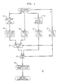
- Fig. 1 there is shown method 10 for preparation of a tantalum surface for use as a counterelectrode in tantalum "wet slug" capacitors.
- Method 10 may proceed by four paths, labelled 10a, 10b, 10c, and 10d.
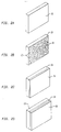
- Figs. 2A-2D show the surface of a portion of tantalum 20 being treated according to method 10 of the present invention.
- Method 10 may be used on stock from which cases are to be drawn. With appropriate fixturing and technique, method 10 may also be applied to the inner surface of already drawn cases or any other tantalum surface.
- the surface of tantalum 20 to be processed is treated with a solution containing a small amount of hydrofluoric acid to remove or destroy the existing air oxide which has formed on the surface of tantalum 20.
- the surface of tantalum 20 is also treated with an activator such as a stannous salt or an organic reducing agent.
- the activator reacts with the surface of tantalum 20, wets and cleans it, and provides seeding for adherence of materials required to destroy the oxidizing ability of the surface of tantalum 20.
- a non-continuous layer of small island-like structures 22 of a member of the platinum group of metals is deposited upon the surface of tantalum 20 using conventional electroless plating solution techniques as shown in Fig. 2B. Discontinuous sections or islands 22 are formed, rather than a continuous layer of the platinum group member, because, even after activation, it is extremely difficult to deposit a platinum group member upon a tantalum surface using electroless plating methods. Coverage of as little as 20% of the surface with islands 22 can be sufficient.
- the members of the platinum group which are believed to be suitable for the capacitor counter-electrode of the present invention include Ru, Rh, Pd, Os, Ir, and Pt. It is also believed that of the members of the platinum group, palladium is preferred because it results in the highest inherent capacitance and thereby provides the most efficient capacitor.
- Deposit 22 is alloyed with the surface of tantalum 20 in block 15 by heat treatment thereby mixing the member of the platinum group with the tantalum at a molecular lever.
- the alloying step of block 15 forms alloy layer 24 as shown in Fig. 2C.
- the heat treatment of block 15 is performed in a vacuum or in an inert atmosphere to prevent oxidation of tantalum 20.
- the temperature required to perform this alloying depends on which member of the platinum group is used.
- the lower temperature limit for each member of the platinum group is that temperature which gives enough alloying to ensure adherence of the deposited platinum group member. This is required to destroy the ability of the tantalum surface to form a dielectric oxide as previously described.
- the upper temperature limit for each member is more difficult to determine than the lower limit. It is believed that bulk alloying is not desirable and that the temperature should not be raised to a level which causes bulk alloying. Furthermore, the temperature should be kept below a level which would cause appreciable loss of material through vaporization.
- a suitable temperature range for alloying palladium with tantalum may be about 825° to about 1400°C
- a suitable temperature range may be about 925° to about 1500°C
- that for alloying rhodium to tantalum a suitable temperature range may be about 975° to about 1650°C.
- osmium and iridium require higher temperatures. It will be understood by those skilled in the art that alloying temperatures may be chosen appropriately for the specific combination of metals selected.
- these temperatures are limited by the type of materials upon which method 10 is performed. For example, if method 10 is performed upon tantalum 20 which is part of a clad of tantalum and some other metal the maximum temperature of alloying must be below approximately 1000°C to prevent damage to the cladding bond.
- alloy layer 24 adhering to the surface of tantalum 20, is formed as previously described.
- the resulting alloy layer 24 may still be discontinuous.
- the alloy surface may be composed of as little as 0.25 atomic percent and still give satisfactory results.
- the surface of alloy layer 24 is suitable for electrodeposition of a member of the platinum group upon alloy layer 24.
- the platinum group member may be sputtered onto the surface of tantalum 20 as shown in blocks 13b and 13c. It is believed that if the original oxide layer from the surface of tantalum 20 is removed, by glow discharge as shown in block 11c of path 10c of method 10, the sputtering of block 13c may result in a mixing of the tantalum and the sputtered material at the molecular level thereby eliminating the alloying step of block 15 to form alloy layer 25 since the material sputtered onto tantalum 20 forms layer 24 if the sputtering energy is high enough.
- the sputtered member of the platinum group forms deposits 22 as previously described and the alloying step of block 15 is required to form alloy layer 24 because the oxide layer remains between the sputtered material and tantalum 20.
- a tantalum-platinum group member alloy may be sputtered directly onto tantalum 20 thereby eliminating the alloying step of block 15.
- the platinum family metal may be clad, as by roll bonding, to the tantalum.
- the cladding forms an alloy of tantalum and the platinum family member and, if the platinum family metal is sufficiently thin, the alloy layer will be discontinuous, as a result of the molecular interpenetration of the two materials.
- the cladding may be conducted by explosive bonding, preferably by roll bonding.
- the tantalum surface may be cleaned first.
- Either hot or cold roll bonding may be employed.
- One or more additional hot or cold rolling steps with intermediate anneals may be carried out to obtain the desired gauge.
- the hot roll bonding technique may be used to form the alloy directly, thus avoiding the need for the separate heat treat/alloy step 15.
- Secondary layer 26 may be any member of the platinum group and need not necessarily be the same platinum group member that was alloyed with tantalum 20 in alloy layer 24. Secondary layer 26 may be formed using conventional electrolytic or electroless techniques since it must adhere to platinum or platinum group member alloy layer 24 rather than to a tantalum surface.
- the deposition of secondary layer 26 shown in block 19 is performed under conditions that produce a spongy physical structure. It is well known in the art how to choose electrical current levels during deposition and how to choose plating solutions in order to provide a spongy surface rather than a smooth surface for layer 26.
- the spongy surface is preferred because it provides more surface area for electrical contact with an electrolyte.
- Layers 24,26 are highly adherent to tantalum 20 and therefore layers 24,26 are highly adherent to a case wall of a capacitor formed using method 10. This eliminates the problem of conductive particles becoming free and mixing in with the electrolyte and maintains the stability of the electrical properties of the counterelectrode.
- tantalum 20 is provided with a surface layer 24 which destroys the oxidizing ability of tantalum 20 wherein surface layer 24 over tantalum 20 has an inherently high effective capacitance. Because of this inherently high effective capacitance, capacitors produced with tantalum 20 treated in accordance with method 10 have a reduced reliance on depolarizing agents.
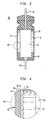
- capacitor 50 which may include a counterelectrode made according to method 10 of the present invention. It will be understood by those skilled in the art that a counterelectrode made in accordance with method 10 may be used in any other type of wet slug capacitor and that capacitor 50 is merely used by way of illustration.
- Capacitor 50 includes porous tantalum anode 38 which is mounted in vibration spacer 40 in the bottom of can 42. The space between gasket 36 and spacer 40 is filled with an electrolyte 37 which impregnates anode 38. Leads 32,34 are electrically coupled to anode 38 and counterelectrode can 42.
- Can 42 includes nickel or nickel alloy layer 44, copper layer 46, and tantalum layer 20 as shown in magnified portion 48. Tantalum layer 20 has been treated in accordance to method 10 of the present invention to provide alloy layer 24 and spongy secondary layer 26.
- method 10 is performed using electroless deposition as shown in path 10a of method 10, by sputtering as shown in paths 10b and 10c, or by cladding as shown in path 10d, all the steps of method 10 may be used either on strip stock before drawing of a capacitor case such as case 42 or on the finished capacitor case itself in which case the step of block 17 is not required.
- the deposition of secondary layer 26 onto the alloyed surface of layer 24 however must be done on finished case 42 to prevent mechanical damage to layer 26.
- paths 10a,b,c, and d are partly determined by cost. It is believed that the sputtering of paths 10b,c is preferred to the deposition of path 10a. However, sputtering equipment involves a much larger initial cost. Avoiding the deposition of path 10a is preferred, for example, when processing strip stock because one side of strip stock must be masked when chemically treating the other side.
- method 10 may be performed upon full tantalum cases as well as those having a laminated or clad structure with tantalum as the inner layer such as case 42 having laminations including nickel layer 44 and copper layer 46. If method 10 is used in making a clad can the layers are first bonded then sputtering or electroless deposition is performed and the alloying is performed but alloying is limited to one thousand degrees, whether on a can or on strip stock, to prevent damage to the laminations. When the alloying is performed the can is drawn as shown in block 17. Method 10 may also be performed upon a counterelectrode foil (not shown) in a foil-type tantalum capacitor (not shown).
- the preferred use for method 10 is in a tri-clad can such as can 42 of capacitor 50 in which a copper layer 46 is disposed between an inner tantalum layer 20 and an outer nickel alloy layer 44.
- a copper layer 46 is disposed between an inner tantalum layer 20 and an outer nickel alloy layer 44.
- the outer nickel alloy layer 44 is an alloy of nickel and copper.
Landscapes
- Engineering & Computer Science (AREA)
- Power Engineering (AREA)
- Chemical & Material Sciences (AREA)
- Materials Engineering (AREA)
- Microelectronics & Electronic Packaging (AREA)
- Fixed Capacitors And Capacitor Manufacturing Machines (AREA)
- Chemically Coating (AREA)
Claims (13)
- Gegenelektrode für einen elektrolytischen Tantal-Kondensator, der eine innere Tantalfläche (20) mit einer hochwirksamen Eigenkapazität hat, dadurch gekennzeichnet, daß über der Tantalfläche (20) eine erste Legierungsschicht (24) aus Tantal und einem Metall der Platinfamilie ausgebildet ist.
- Gegenelektrode nach Anspruch 1, dadurch gekennzeichnet, daß über der ersten Legierungsschicht (24) eine zweite Schicht (26) aus einem Metall der Platinfamilie ausgebildet ist.
- Verfahren zum Herstellen einer hochwirksamen Eigenkapazität-Gegenelektrodenfläche (20) auf Tantal zur Verwendung bei einem elektrolytischen Kondensator, gekennzeichnet. durch:(a) Zerstäubung einer Schicht eines ersten Metalls der Platinfamilie über dem Tantal, um auf dem Tantal Niederschläge (22) des ersten Metalls der Platinfamilie auszubilden; und(b) Hitzebehandlung, um eine erste Legierungsschicht (24) aus Tantal und dem ersten Metall der Platinfamilie auszubilden.
- Verfahren zum Herstellen einer hochwirksamen Eigenkapazität-Gegenelektrodenfläche (20) auf Tantal zur Verwendung bei einem elektrolytischen Kondensator, gekennzeichnet durch:(a) Entfernung eines vorhandenen Oxyds von dem Tantal; und(b) Zerstäubung einer Schicht eines ersten Metalls der Platinfamilie über dem Tantal, um eine erste Legierungsschicht (24) aus Tantal und dem esten Metall der Platinfamilie auszubilden.
- Verfahren zum Herstellen einer hochwirksamen Eigenkapazität-Gegenelektrodenfläche (20) auf Tantal zur Verwendung bei einem elektrolytischen Kondensator, gekennzeichnet durch:
Plattieren einer dünnen Schicht eines Metalls der Platinfamilie auf Tantal, wodurch eine erste Legierungsschicht (24) aus Tantal und dem ersten Metall der Platinfamilie ausgebildet wird. - Verfahren nach Anspruch 5, bei welchem die Stufe des Plattierens Weiterhin gekennzeichnet ist durch eine Warmwalzbindung.
- Verfahren zum Herstellen einer hochwirksamen Eigenkapazität-Gegenelektrodenfläche (20) auf Tantal zur Verwendung bei einem elektrolytischen Kondensator, gekennzeichnet durch:(a) Plattieren einer dünnen Schicht eines Metalls der Platinfamilie auf dem Tantal; und(b) Hitzebehandlung, um eine erste Legierungsschicht (24) aus Tantal und dem ersten Metall der Platinfamilie auszubilden.
- Verfahren nach Anspruch 7, bei welchem die Stufe des Plattierens weiterhin gekennzeichnet ist durch eine Warmwalzbindung.
- Verfahren zum Herstellen einer hochwirksamen Eigenkapazität-Gegenelektrodenfläche (20) auf Tantal zur Verwendung bei einem elektrolytischen Kondensator, gekennzeichnet durch:(a) Entfernung eines vorhandenen Oxyds von dem Tantal;(b) Niederschlag einer unterbrochenen Schicht (22) eines ersten Metalls der Platinfamilie über dem Tantal; und(c) Legieren des niedergeschlagenen ersten Metalls mit dem Tantal, um eine Legierungsschicht (24) auszubilden.
- Verfahren nach Anspruch 9, bei welchem die Stufe (c) weiterhin gekennzeichnet ist durch ein Niederschlagen einer Schicht (26) eines zweiten Metalls der Platinfamilie über der Legierungsschicht (24).
- Verfahren nach Anspruch 9, dadurch gekennzeichnet, daß die Stufe (a) eine Behandlung der Tantalfläche mit einer Säure umfaßt.
- Verfahren nach Anspruch 11, dadurch gekennzeichnet, daß die Säure Fluorwasserstoffsäure ist.
- Verfahren nach Anspruch 9, bei welchem die Stufe (b) gekennzeichnet ist durch ein stromloses Plattieren der Tantalfläche.
Priority Applications (1)
| Application Number | Priority Date | Filing Date | Title |
|---|---|---|---|
| AT88311896T ATE89948T1 (de) | 1987-12-16 | 1988-12-16 | Kondensatortantaloberflaeche zur verwendung als gegenelektrodenanordnung und verfahren. |
Applications Claiming Priority (6)
| Application Number | Priority Date | Filing Date | Title |
|---|---|---|---|
| US133547 | 1987-12-16 | ||
| US07/133,547 US4780797A (en) | 1987-12-16 | 1987-12-16 | Capacitor tantalum surface for use as a counterelectrode device and method |
| US21863588A | 1988-07-13 | 1988-07-13 | |
| US218635 | 1988-07-13 | ||
| US319556 | 1988-12-12 | ||
| US07/319,556 US4942500A (en) | 1988-07-13 | 1988-12-12 | Capacitor tantalum surface for use as a counterelectrode device and method |
Publications (2)
| Publication Number | Publication Date |
|---|---|
| EP0321255A1 EP0321255A1 (de) | 1989-06-21 |
| EP0321255B1 true EP0321255B1 (de) | 1993-05-26 |
Family
ID=27384443
Family Applications (1)
| Application Number | Title | Priority Date | Filing Date |
|---|---|---|---|
| EP19880311896 Expired - Lifetime EP0321255B1 (de) | 1987-12-16 | 1988-12-16 | Kondensatortantaloberfläche zur Verwendung als Gegenelektrodenanordnung und Verfahren |
Country Status (3)
| Country | Link |
|---|---|
| EP (1) | EP0321255B1 (de) |
| JP (1) | JPH04127411A (de) |
| DE (1) | DE3881359T2 (de) |
Families Citing this family (3)
| Publication number | Priority date | Publication date | Assignee | Title |
|---|---|---|---|---|
| FR2685080B1 (fr) * | 1991-12-17 | 1995-09-01 | Thomson Csf | Capteur mecanique comprenant un film de polymere. |
| JP5665730B2 (ja) * | 2008-03-20 | 2015-02-04 | ヴィシェイ スプラーグ インコーポレイテッド | 電解コンデンサとその製造方法 |
| CN110957138B (zh) * | 2019-11-18 | 2024-04-16 | 湖南华冉科技有限公司 | 钽电容器外壳的内壁处理方法 |
Family Cites Families (4)
| Publication number | Priority date | Publication date | Assignee | Title |
|---|---|---|---|---|
| US3616445A (en) * | 1967-12-14 | 1971-10-26 | Electronor Corp | Titanium or tantalum base electrodes with applied titanium or tantalum oxide face activated with noble metals or noble metal oxides |
| US4020401A (en) * | 1975-12-19 | 1977-04-26 | General Electric Company | Electrolytic capacitor having a silver plated nickel case |
| US4523255A (en) * | 1983-09-19 | 1985-06-11 | Sprague Electric Company | Cathode for an electrolytic capacitor |
| US4780797A (en) * | 1987-12-16 | 1988-10-25 | Tansitor Electronic, Inc. | Capacitor tantalum surface for use as a counterelectrode device and method |
-
1988
- 1988-12-16 JP JP31654988A patent/JPH04127411A/ja active Pending
- 1988-12-16 EP EP19880311896 patent/EP0321255B1/de not_active Expired - Lifetime
- 1988-12-16 DE DE19883881359 patent/DE3881359T2/de not_active Expired - Lifetime
Also Published As
| Publication number | Publication date |
|---|---|
| JPH04127411A (ja) | 1992-04-28 |
| DE3881359D1 (de) | 1993-07-01 |
| DE3881359T2 (de) | 1994-01-20 |
| EP0321255A1 (de) | 1989-06-21 |
Similar Documents
| Publication | Publication Date | Title |
|---|---|---|
| US4780797A (en) | Capacitor tantalum surface for use as a counterelectrode device and method | |
| US4942500A (en) | Capacitor tantalum surface for use as a counterelectrode device and method | |
| EP0940828B1 (de) | Verfahren zum Herstellen von Folien-Elektroden | |
| US6391773B2 (en) | Method and materials for through-mask electroplating and selective base removal | |
| KR100975757B1 (ko) | 적층형 전자부품 및 그 제조방법 | |
| US4523255A (en) | Cathode for an electrolytic capacitor | |
| JPS62133738A (ja) | 集積回路 | |
| EP0168828A2 (de) | Verfahren zum Herstellen einer Halbleiteranordnung mit Leiterschichten | |
| US20070260282A1 (en) | Feedthrough apparatus with noble metal-coated leads | |
| JP5493328B2 (ja) | 積層型電子部品の製造方法 | |
| US6096391A (en) | Method for improving electrical conductivity of metals, metal alloys and metal oxides | |
| US4910638A (en) | Ceramic multilayer capacitor | |
| US5926360A (en) | Metallized oxide structure and fabrication | |
| EP0321255A1 (de) | Kondensatortantaloberfläche zur Verwendung als Gegenelektrodenanordnung und Verfahren | |
| JP3439064B2 (ja) | 固体電解コンデンサ | |
| US4615908A (en) | Method for the manufacture of plasma-polymer multilayer capacitors | |
| KR20060032210A (ko) | 적층형 세라믹 전자부품 및 그 제조방법 | |
| US20030070920A1 (en) | Electrode for use in a capacitor | |
| JP5217609B2 (ja) | 積層セラミック電子部品およびその製造方法 | |
| JP2004524686A (ja) | 電解コンデンサーおよびその作製方法 | |
| JPH0241885B2 (de) | ||
| JP3016353B2 (ja) | 薄膜回路素子およびその製造方法 | |
| JPH09186054A (ja) | 電解コンデンサ用アルミニウム陰極箔 | |
| JP2008252019A (ja) | 薄膜キャパシタの製造方法 | |
| JP3524298B2 (ja) | 積層セラミックコンデンサの外部電極の形成方法 |
Legal Events
| Date | Code | Title | Description |
|---|---|---|---|
| PUAI | Public reference made under article 153(3) epc to a published international application that has entered the european phase |
Free format text: ORIGINAL CODE: 0009012 |
|
| AK | Designated contracting states |
Kind code of ref document: A1 Designated state(s): AT BE CH DE ES FR GB GR IT LI LU NL SE |
|
| 17P | Request for examination filed |
Effective date: 19891215 |
|
| 17Q | First examination report despatched |
Effective date: 19920203 |
|
| GRAA | (expected) grant |
Free format text: ORIGINAL CODE: 0009210 |
|
| AK | Designated contracting states |
Kind code of ref document: B1 Designated state(s): AT BE CH DE ES FR GB GR IT LI LU NL SE |
|
| PG25 | Lapsed in a contracting state [announced via postgrant information from national office to epo] |
Ref country code: IT Free format text: LAPSE BECAUSE OF FAILURE TO SUBMIT A TRANSLATION OF THE DESCRIPTION OR TO PAY THE FEE WITHIN THE PRE;WARNING: LAPSES OF ITALIAN PATENTS WITH EFFECTIVE DATE BEFORE 2007 MAY HAVE OCCURRED AT ANY TIME BEFORE 2007. THE CORRECT EFFECTIVE DATE MAY BE DIFFERENT FROM THE ONE RECORDED.SCRIBED TIME-LIMIT Effective date: 19930526 Ref country code: BE Effective date: 19930526 Ref country code: CH Effective date: 19930526 Ref country code: ES Free format text: THE PATENT HAS BEEN ANNULLED BY A DECISION OF A NATIONAL AUTHORITY Effective date: 19930526 Ref country code: AT Effective date: 19930526 Ref country code: LI Effective date: 19930526 Ref country code: GR Free format text: LAPSE BECAUSE OF FAILURE TO SUBMIT A TRANSLATION OF THE DESCRIPTION OR TO PAY THE FEE WITHIN THE PRESCRIBED TIME-LIMIT Effective date: 19930526 Ref country code: SE Effective date: 19930526 Ref country code: NL Effective date: 19930526 |
|
| REF | Corresponds to: |
Ref document number: 89948 Country of ref document: AT Date of ref document: 19930615 Kind code of ref document: T |
|
| REF | Corresponds to: |
Ref document number: 3881359 Country of ref document: DE Date of ref document: 19930701 |
|
| REG | Reference to a national code |
Ref country code: CH Ref legal event code: PL |
|
| ET | Fr: translation filed | ||
| NLV1 | Nl: lapsed or annulled due to failure to fulfill the requirements of art. 29p and 29m of the patents act | ||
| PGFP | Annual fee paid to national office [announced via postgrant information from national office to epo] |
Ref country code: LU Payment date: 19931231 Year of fee payment: 6 |
|
| PLBE | No opposition filed within time limit |
Free format text: ORIGINAL CODE: 0009261 |
|
| STAA | Information on the status of an ep patent application or granted ep patent |
Free format text: STATUS: NO OPPOSITION FILED WITHIN TIME LIMIT |
|
| 26N | No opposition filed | ||
| PG25 | Lapsed in a contracting state [announced via postgrant information from national office to epo] |
Ref country code: LU Free format text: LAPSE BECAUSE OF NON-PAYMENT OF DUE FEES Effective date: 19941216 |
|
| REG | Reference to a national code |
Ref country code: GB Ref legal event code: IF02 |
|
| PGFP | Annual fee paid to national office [announced via postgrant information from national office to epo] |
Ref country code: GB Payment date: 20071106 Year of fee payment: 20 |
|
| PGFP | Annual fee paid to national office [announced via postgrant information from national office to epo] |
Ref country code: DE Payment date: 20071228 Year of fee payment: 20 |
|
| PGFP | Annual fee paid to national office [announced via postgrant information from national office to epo] |
Ref country code: FR Payment date: 20071204 Year of fee payment: 20 |
|
| REG | Reference to a national code |
Ref country code: GB Ref legal event code: PE20 Expiry date: 20081215 |
|
| PG25 | Lapsed in a contracting state [announced via postgrant information from national office to epo] |
Ref country code: GB Free format text: LAPSE BECAUSE OF EXPIRATION OF PROTECTION Effective date: 20081215 |