EP0321327A1 - Verfahren zum Plazieren einer elektronischen Komponente und seiner elektronsichen Verbindungen auf einer Unterlage - Google Patents
Verfahren zum Plazieren einer elektronischen Komponente und seiner elektronsichen Verbindungen auf einer Unterlage Download PDFInfo
- Publication number
- EP0321327A1 EP0321327A1 EP88403140A EP88403140A EP0321327A1 EP 0321327 A1 EP0321327 A1 EP 0321327A1 EP 88403140 A EP88403140 A EP 88403140A EP 88403140 A EP88403140 A EP 88403140A EP 0321327 A1 EP0321327 A1 EP 0321327A1
- Authority
- EP
- European Patent Office
- Prior art keywords
- electronic component
- metal
- layer
- support
- polyimide
- Prior art date
- Legal status (The legal status is an assumption and is not a legal conclusion. Google has not performed a legal analysis and makes no representation as to the accuracy of the status listed.)
- Granted
Links
Images
Classifications
-
- G—PHYSICS
- G06—COMPUTING OR CALCULATING; COUNTING
- G06K—GRAPHICAL DATA READING; PRESENTATION OF DATA; RECORD CARRIERS; HANDLING RECORD CARRIERS
- G06K19/00—Record carriers for use with machines and with at least a part designed to carry digital markings
- G06K19/06—Record carriers for use with machines and with at least a part designed to carry digital markings characterised by the kind of the digital marking, e.g. shape, nature, code
- G06K19/067—Record carriers with conductive marks, printed circuits or semiconductor circuit elements, e.g. credit or identity cards also with resonating or responding marks without active components
- G06K19/07—Record carriers with conductive marks, printed circuits or semiconductor circuit elements, e.g. credit or identity cards also with resonating or responding marks without active components with integrated circuit chips
- G06K19/077—Constructional details, e.g. mounting of circuits in the carrier
- G06K19/07745—Mounting details of integrated circuit chips
-
- H—ELECTRICITY
- H10—SEMICONDUCTOR DEVICES; ELECTRIC SOLID-STATE DEVICES NOT OTHERWISE PROVIDED FOR
- H10W—GENERIC PACKAGES, INTERCONNECTIONS, CONNECTORS OR OTHER CONSTRUCTIONAL DETAILS OF DEVICES COVERED BY CLASS H10
- H10W70/00—Package substrates; Interposers; Redistribution layers [RDL]
- H10W70/60—Insulating or insulated package substrates; Interposers; Redistribution layers
- H10W70/699—Insulating or insulated package substrates; Interposers; Redistribution layers for flat cards, e.g. credit cards
-
- H—ELECTRICITY
- H10—SEMICONDUCTOR DEVICES; ELECTRIC SOLID-STATE DEVICES NOT OTHERWISE PROVIDED FOR
- H10W—GENERIC PACKAGES, INTERCONNECTIONS, CONNECTORS OR OTHER CONSTRUCTIONAL DETAILS OF DEVICES COVERED BY CLASS H10
- H10W72/00—Interconnections or connectors in packages
- H10W72/50—Bond wires
-
- H—ELECTRICITY
- H10—SEMICONDUCTOR DEVICES; ELECTRIC SOLID-STATE DEVICES NOT OTHERWISE PROVIDED FOR
- H10W—GENERIC PACKAGES, INTERCONNECTIONS, CONNECTORS OR OTHER CONSTRUCTIONAL DETAILS OF DEVICES COVERED BY CLASS H10
- H10W72/00—Interconnections or connectors in packages
- H10W72/071—Connecting or disconnecting
- H10W72/075—Connecting or disconnecting of bond wires
-
- H—ELECTRICITY
- H10—SEMICONDUCTOR DEVICES; ELECTRIC SOLID-STATE DEVICES NOT OTHERWISE PROVIDED FOR
- H10W—GENERIC PACKAGES, INTERCONNECTIONS, CONNECTORS OR OTHER CONSTRUCTIONAL DETAILS OF DEVICES COVERED BY CLASS H10
- H10W72/00—Interconnections or connectors in packages
- H10W72/50—Bond wires
- H10W72/541—Dispositions of bond wires
- H10W72/5449—Dispositions of bond wires not being orthogonal to a side surface of the chip, e.g. fan-out arrangements
-
- H—ELECTRICITY
- H10—SEMICONDUCTOR DEVICES; ELECTRIC SOLID-STATE DEVICES NOT OTHERWISE PROVIDED FOR
- H10W—GENERIC PACKAGES, INTERCONNECTIONS, CONNECTORS OR OTHER CONSTRUCTIONAL DETAILS OF DEVICES COVERED BY CLASS H10
- H10W72/00—Interconnections or connectors in packages
- H10W72/90—Bond pads, in general
- H10W72/931—Shapes of bond pads
- H10W72/932—Plan-view shape, i.e. in top view
-
- H—ELECTRICITY
- H10—SEMICONDUCTOR DEVICES; ELECTRIC SOLID-STATE DEVICES NOT OTHERWISE PROVIDED FOR
- H10W—GENERIC PACKAGES, INTERCONNECTIONS, CONNECTORS OR OTHER CONSTRUCTIONAL DETAILS OF DEVICES COVERED BY CLASS H10
- H10W90/00—Package configurations
- H10W90/701—Package configurations characterised by the relative positions of pads or connectors relative to package parts
- H10W90/751—Package configurations characterised by the relative positions of pads or connectors relative to package parts of bond wires
- H10W90/754—Package configurations characterised by the relative positions of pads or connectors relative to package parts of bond wires between a chip and a stacked insulating package substrate, interposer or RDL
-
- Y—GENERAL TAGGING OF NEW TECHNOLOGICAL DEVELOPMENTS; GENERAL TAGGING OF CROSS-SECTIONAL TECHNOLOGIES SPANNING OVER SEVERAL SECTIONS OF THE IPC; TECHNICAL SUBJECTS COVERED BY FORMER USPC CROSS-REFERENCE ART COLLECTIONS [XRACs] AND DIGESTS
- Y10—TECHNICAL SUBJECTS COVERED BY FORMER USPC
- Y10T—TECHNICAL SUBJECTS COVERED BY FORMER US CLASSIFICATION
- Y10T29/00—Metal working
- Y10T29/49—Method of mechanical manufacture
- Y10T29/49002—Electrical device making
- Y10T29/49117—Conductor or circuit manufacturing
- Y10T29/49124—On flat or curved insulated base, e.g., printed circuit, etc.
- Y10T29/4913—Assembling to base an electrical component, e.g., capacitor, etc.
- Y10T29/49144—Assembling to base an electrical component, e.g., capacitor, etc. by metal fusion
Definitions
- the invention relates to a method of placing an electronic component and its electrical connections on a support such as an identification card or a bank card; it also relates to the product obtained by implementing this process.
- the card comprises an active electronic component which can consist of an electronic memory associated or not with a microprocessor, which makes it possible to use it in particular for banking type applications.
- the prior art cards which include an electronic component are produced in various ways.
- a cavity is arranged in the thickness of the card to receive the electronic component.
- thin layers of plastic are laminated: polyepoxy, polyethylene, polyvinyl chloride, etc. around the component.
- various operations are in in addition carried out to ensure the electrical connection of the terminals of the electronic component to metallizations which are arranged on the surface on the card.
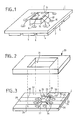
- One of the methods for placing the electronic component in the cavity provided in the card and for placing the metallizations on the card as well as for making the connections between the terminals of the card and the metallizations consists, as shown in FIG. 1 , to use a non-conductive film 1, for example made of polyepoxy, which carries, on the one hand, the electronic component in the form of a chip referenced 2 and, on the other side, metallized surfaces such as those referenced 3, 4 and 5 and separated from each other by spaces 6 and 7 without metallization.
- These metallized surfaces 3, 4 and 5 communicate with the other side of the film 1 through holes 8, 9 and 10 by means of which the ends of conductive wires 11, 12 and 13 are connected to the corresponding metallized surfaces by any means. known such as a conductive adhesive.
- the other end of each conductive wire is connected to an output terminal 14, 15 or 16 of chip 2.
- the object of the present invention is therefore to remedy the aforementioned drawbacks by implementing a method of placing an electronic component and its electrical connections on a support which allows a higher baking temperature of the coating resin. , hence a shorter cooking time and therefore a lower cost.
- the invention also relates to a product obtained by implementing the method which comprises a support card provided with a cavity and an electronic component disposed in said cavity, characterized in that said electronic component is disposed directly on a metal layer, which is stuck on the card, and that this metal layer is divided into zones each corresponding to a contact.
- the product obtained has an electronic component which is fixed to the metallitic layer by means of a polyimide layer.
- Figure 1 corresponds to the prior art and has been described in the preamble.
- a memory card 20 which has in its middle a cavity 21 in which must be housed an electronic component, for example the chip 2 in FIG. 1.
- an electronic component for example the chip 2 in FIG. 1.
- the support film 1 is replaced by a layer of metal 22, for example copper or nickel, having a thickness of a few tens of microns, for example eighty microns.
- This metal layer 22, deposited on a work support (not shown), is cut along the line which is indicated by the segments 23 to 30 connected to the center by a circular cut 31.
- This cutting can be carried out by any known means and in particular by a chemical process such as etching or a mechanical process using a laser device.
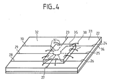
- These different segments 23 to 31 delimit metal zones such as those referenced 32 and 33, which are electrically separated so as to act as contacts. So that these different zones do not separate from each other, a layer 34 of polyimide or silicone is deposited over their entire surface. This deposition is carried out in the liquid phase on the metal and adheres naturally to the latter without modifying the structure of the metal and of the metal zones.
- polyimide or silicone epoxy resin can be used which is deposited at very high temperature. The thickness of this polyimide layer is approximately a few microns, for example three microns. In Figure 3, this polyimide layer is assumed to be transparent.
- the following operation consists in placing and gluing an electronic component 35 on the metal layer 22.
- two solutions are possible: one is to turn the assembly of FIG. 3 so that the polyimide layer 34 is in contact with the working support (FIG. 4), the other is to remove the polyimide layer where the component 35 must be bonded by any known method, for example by chemical attack with mask.
- the mask is provided for removing the polyimide layer, not only at the location of the component 35, but also at the locations 36 where the electrical connections between the component and the metal areas must be made.
- the component 35 is bonded to said area using an adhesive which resists high temperatures.
- This bonding operation of the component 35 is followed by an electrical connection operation of each of the output terminals 37 of the chip 35 to a metal area 32 by means of a conductive wire 38.
- the connection of the ends of each wire conductive can be carried out by any known means, for example by bonding using a conductive adhesive.
- the assembly - polyimide layer 34 and metal layer 22 carrying the electronic component 35 and the electrical connections 38 - is ready to carry out the operation of encapsulation of the electronic component 35 and the electrical connections by any process known, in particular molding in a resin and then heating the assembly to harden the resin and obtain a compact block (not shown). Due to the absence of a support film for the metal layer and of a retaining adhesive between this metal layer and the support film, elements which do not withstand temperatures above 150 ° C, the assembly of each of Figures 3 and 4 can be heated to temperatures in the region of 300 ° C, which considerably accelerates the hardening process of the encapsulation resin. The result is a simpler automatic production line, saving time and money.
- the metal component-layer assembly is put in place on the card 20 (FIG. 2) so that the compact block containing the component 35 and its electrical connections fits into the cavity 21 and that the metal zones come to rest on the edges of the cavity where they are fixed by any known method, in particular by gluing. It will be noted that these metal zones rest directly on the edges of the cavity 21 in the case of FIG. 4 but through the polyimide layer 34 in the case of FIG. 3.
- this layer must be removed to expose the metal areas so that they play their role of electrical contacts .
- This removal can be carried out by any known method, for example by chemical attack without mask, or again by a mechanical method such as polishing.
- This cleaning operation can be carried out before or after the installation of the component-metal layer assembly on the menu. In this cleaning, the underlying polyimide layer 34 should not be damaged.
- the polyimide occupying the spaces between the metal areas is also removed, so that said areas appear in relief on the center of the support 20 and that 'there may be communication holes between the cavity 21 and the environment external to the card.
- the polyimide layer 34 remains in place in the final device. According to a variant of the method, it can be removed before the assembly of the assembly on the card but, in this case, it must be taken into account that the mechanical strength of the metal areas is less good. To remedy this problem, it is proposed to leave the polyimide seals in place between said zones and to replace the polyimide layer with a layer of adhesive which serves to fix the assembly on the card.
Landscapes
- Engineering & Computer Science (AREA)
- Computer Hardware Design (AREA)
- Microelectronics & Electronic Packaging (AREA)
- Physics & Mathematics (AREA)
- General Physics & Mathematics (AREA)
- Theoretical Computer Science (AREA)
- Credit Cards Or The Like (AREA)
- Wire Bonding (AREA)
- Encapsulation Of And Coatings For Semiconductor Or Solid State Devices (AREA)
Applications Claiming Priority (2)
| Application Number | Priority Date | Filing Date | Title |
|---|---|---|---|
| FR8717386 | 1987-12-14 | ||
| FR8717386A FR2624651B1 (fr) | 1987-12-14 | 1987-12-14 | Procede de mise en place d'un composant electronique et de ses connexions electriques sur un support et produit ainsi obtenu |
Publications (2)
| Publication Number | Publication Date |
|---|---|
| EP0321327A1 true EP0321327A1 (de) | 1989-06-21 |
| EP0321327B1 EP0321327B1 (de) | 1996-04-10 |
Family
ID=9357823
Family Applications (1)
| Application Number | Title | Priority Date | Filing Date |
|---|---|---|---|
| EP88403140A Expired - Lifetime EP0321327B1 (de) | 1987-12-14 | 1988-12-09 | Verfahren zum Plazieren einer elektronischen Komponente und seiner elektronsichen Verbindungen auf einer Unterlage |
Country Status (6)
| Country | Link |
|---|---|
| US (1) | US4908937A (de) |
| EP (1) | EP0321327B1 (de) |
| JP (1) | JP2761501B2 (de) |
| KR (1) | KR890010748A (de) |
| DE (1) | DE3855197T2 (de) |
| FR (1) | FR2624651B1 (de) |
Cited By (2)
| Publication number | Priority date | Publication date | Assignee | Title |
|---|---|---|---|---|
| DE4224103A1 (de) * | 1992-07-22 | 1994-01-27 | Manfred Dr Ing Michalk | Miniaturgehäuse mit elektronischen Bauelementen |
| WO1997044823A1 (de) * | 1996-05-17 | 1997-11-27 | Siemens Aktiengesellschaft | Trägerelement für einen halbleiterchip |
Families Citing this family (10)
| Publication number | Priority date | Publication date | Assignee | Title |
|---|---|---|---|---|
| FR2664721B1 (fr) * | 1990-07-10 | 1992-09-25 | Gemplus Card Int | Carte a puce renforcee. |
| FR2695234B1 (fr) * | 1992-08-26 | 1994-11-04 | Gemplus Card Int | Procédé de marquage d'une carte à puce. |
| US5581445A (en) * | 1994-02-14 | 1996-12-03 | Us3, Inc. | Plastic integrated circuit card with reinforcement structure for protecting integrated circuit module |
| FR2724477B1 (fr) * | 1994-09-13 | 1997-01-10 | Gemplus Card Int | Procede de fabrication de cartes sans contact |
| FR2777675B1 (fr) | 1998-04-15 | 2001-12-07 | Rue Cartes Et Systemes De | Procede de fabrication d'une carte a microcircuit et carte a microcircuit obtenue par mise en oeuvre de ce procede |
| JP4749656B2 (ja) | 2001-02-09 | 2011-08-17 | 台湾積體電路製造股▲ふん▼有限公司 | 半導体デバイスの製造方法及びこの方法により得られる半導体デバイス |
| DE10217262A1 (de) * | 2002-04-18 | 2003-11-06 | Pall Corp | Filtermodul und Verfahren zur Herstellung eines gefüllten Filtermoduls |
| WO2005017421A1 (ja) | 2003-08-01 | 2005-02-24 | Asahi Glass Company, Limited | 太陽熱利用発電システム用被覆資材及びそれを展張した太陽熱利用発電システム |
| US20060175711A1 (en) * | 2005-02-08 | 2006-08-10 | Hannstar Display Corporation | Structure and method for bonding an IC chip |
| DE102007019795B4 (de) * | 2007-04-26 | 2012-10-04 | Infineon Technologies Ag | Chipmodul und Verfahren zum Herstellen dieses Chipmoduls |
Citations (1)
| Publication number | Priority date | Publication date | Assignee | Title |
|---|---|---|---|---|
| EP0128822A1 (de) * | 1983-06-09 | 1984-12-19 | Flonic S.A. | Verfahren zur Herstellung von Speicherkarten und hierdurch hergestellte Karten |
Family Cites Families (5)
| Publication number | Priority date | Publication date | Assignee | Title |
|---|---|---|---|---|
| DE3248385A1 (de) * | 1982-12-28 | 1984-06-28 | GAO Gesellschaft für Automation und Organisation mbH, 8000 München | Ausweiskarte mit integriertem schaltkreis |
| US4567643A (en) * | 1983-10-24 | 1986-02-04 | Sintra-Alcatel | Method of replacing an electronic component connected to conducting tracks on a support substrate |
| JPS6095941A (ja) * | 1983-10-31 | 1985-05-29 | Toshiba Corp | 半導体装置 |
| JPS6115289A (ja) * | 1984-06-29 | 1986-01-23 | Mitsubishi Plastics Ind Ltd | メモリ−カ−ド |
| US4801765A (en) * | 1986-01-06 | 1989-01-31 | American Telephone And Telegraph Company, At&T Bell Laboratories | Electronic component package using multi-level lead frames |
-
1987
- 1987-12-14 FR FR8717386A patent/FR2624651B1/fr not_active Expired - Lifetime
-
1988
- 1988-12-09 EP EP88403140A patent/EP0321327B1/de not_active Expired - Lifetime
- 1988-12-09 DE DE3855197T patent/DE3855197T2/de not_active Expired - Fee Related
- 1988-12-12 KR KR1019880016607A patent/KR890010748A/ko not_active Withdrawn
- 1988-12-12 US US07/283,214 patent/US4908937A/en not_active Ceased
- 1988-12-14 JP JP63316074A patent/JP2761501B2/ja not_active Expired - Lifetime
Patent Citations (1)
| Publication number | Priority date | Publication date | Assignee | Title |
|---|---|---|---|---|
| EP0128822A1 (de) * | 1983-06-09 | 1984-12-19 | Flonic S.A. | Verfahren zur Herstellung von Speicherkarten und hierdurch hergestellte Karten |
Non-Patent Citations (1)
| Title |
|---|
| PATENT ABSTRACTS OF JAPAN * |
Cited By (2)
| Publication number | Priority date | Publication date | Assignee | Title |
|---|---|---|---|---|
| DE4224103A1 (de) * | 1992-07-22 | 1994-01-27 | Manfred Dr Ing Michalk | Miniaturgehäuse mit elektronischen Bauelementen |
| WO1997044823A1 (de) * | 1996-05-17 | 1997-11-27 | Siemens Aktiengesellschaft | Trägerelement für einen halbleiterchip |
Also Published As
| Publication number | Publication date |
|---|---|
| JPH021399A (ja) | 1990-01-05 |
| DE3855197D1 (de) | 1996-05-15 |
| JP2761501B2 (ja) | 1998-06-04 |
| DE3855197T2 (de) | 1996-10-02 |
| FR2624651A1 (fr) | 1989-06-16 |
| FR2624651B1 (fr) | 1991-09-06 |
| US4908937A (en) | 1990-03-20 |
| EP0321327B1 (de) | 1996-04-10 |
| KR890010748A (ko) | 1989-08-10 |
Similar Documents
| Publication | Publication Date | Title |
|---|---|---|
| EP0391790B1 (de) | Herstellungsverfähren für elektronische Module | |
| EP0128822B1 (de) | Verfahren zur Herstellung von Speicherkarten und hierdurch hergestellte Karten | |
| EP0321340B1 (de) | Halter für elektronische Komponenten, insbesondere für Speicherkarten und auf solche Weise hergestelltes Produkt | |
| EP0297991B1 (de) | Verfahren zum Herstellen einer elektronischen Mikroschaltungskarte | |
| EP0197438B1 (de) | Verfahren zur Herstellung von elektronischen Modulen für Karten mit Mikroschaltungen und derartig hergestellte Module | |
| EP0207853B1 (de) | Verfahren zum Montieren einer integrierten Schaltung auf einem Träger, resultierende Anordnung und ihre Anwendung bei einer elektronischen Mikroschaltungskarte | |
| FR2488446A1 (fr) | Element support pour un module de circuits integres | |
| EP0321327B1 (de) | Verfahren zum Plazieren einer elektronischen Komponente und seiner elektronsichen Verbindungen auf einer Unterlage | |
| EP0490739A1 (de) | Verfahren und Anordnung zum Verbinden integrierter Schaltungen in drei Dimensionen | |
| FR2857157A1 (fr) | Procede d'interconnexion de composants actif et passif et composant heterogene a faible epaisseur en resultant | |
| FR2769441A1 (fr) | Carte electronique sans contact et son procede de fabrication | |
| EP0321326B1 (de) | Verfahren zum Anbringen eines elektronischen Bauelementes auf einem Substrat | |
| FR2784210A1 (fr) | Carte a puce sans contact comportant des moyens d'inhibition | |
| EP0226480A1 (de) | Verfahren zur Herstellung eines Mikrogehäuses mit Kontaktflecken und dessen Anwendung für Karten mit elektronischen Bauelementen | |
| FR2618254A1 (fr) | Procede et structure de prise de contact sur des plots de circuit integre. | |
| EP0323295B1 (de) | Verfahren zum Befestigen eines elektronischen Bausteins und seiner Kontakte auf einen Träger | |
| FR2547440A1 (fr) | Procede de fabrication de cartes a memoire et cartes obtenues suivant ce procede | |
| WO2000031686A1 (fr) | Procede de fabrication de carte a puce a contact affleurant utilisant une etape de gravure au laser et carte a puce obtenue par le procede | |
| WO2000077731A1 (fr) | Dispositif et procede de fabrication de dispositifs comprenant au moins une puce montee sur un support | |
| WO2004100063A1 (fr) | Procede de fabrication d'un inlet prelamine | |
| FR2817656A1 (fr) | Isolation electrique de microcircuits regroupes avant collage unitaire | |
| EP1709574A1 (de) | Verfahren zur herstellung eines elektronischen schlüssels mit usb-verbinder und erhaltener elektronischer schlüssel | |
| WO2000077727A1 (fr) | Module comportant au moins une puce et son interface de communication, objet comportant un module et procede de realisation desdits modules | |
| WO2000079478A1 (fr) | Procede pour la fabrication d'un module pour cartes a puces et module obtenu |
Legal Events
| Date | Code | Title | Description |
|---|---|---|---|
| PUAI | Public reference made under article 153(3) epc to a published international application that has entered the european phase |
Free format text: ORIGINAL CODE: 0009012 |
|
| AK | Designated contracting states |
Kind code of ref document: A1 Designated state(s): DE ES GB IT NL |
|
| 17P | Request for examination filed |
Effective date: 19890725 |
|
| 17Q | First examination report despatched |
Effective date: 19920331 |
|
| GRAA | (expected) grant |
Free format text: ORIGINAL CODE: 0009210 |
|
| AK | Designated contracting states |
Kind code of ref document: B1 Designated state(s): DE ES GB IT NL |
|
| PG25 | Lapsed in a contracting state [announced via postgrant information from national office to epo] |
Ref country code: NL Free format text: LAPSE BECAUSE OF FAILURE TO SUBMIT A TRANSLATION OF THE DESCRIPTION OR TO PAY THE FEE WITHIN THE PRESCRIBED TIME-LIMIT Effective date: 19960410 |
|
| REF | Corresponds to: |
Ref document number: 3855197 Country of ref document: DE Date of ref document: 19960515 |
|
| ITF | It: translation for a ep patent filed | ||
| GBT | Gb: translation of ep patent filed (gb section 77(6)(a)/1977) |
Effective date: 19960507 |
|
| PG25 | Lapsed in a contracting state [announced via postgrant information from national office to epo] |
Ref country code: ES Free format text: LAPSE BECAUSE OF FAILURE TO SUBMIT A TRANSLATION OF THE DESCRIPTION OR TO PAY THE FEE WITHIN THE PRESCRIBED TIME-LIMIT Effective date: 19960721 |
|
| NLV1 | Nl: lapsed or annulled due to failure to fulfill the requirements of art. 29p and 29m of the patents act | ||
| PGFP | Annual fee paid to national office [announced via postgrant information from national office to epo] |
Ref country code: ES Payment date: 19961228 Year of fee payment: 9 |
|
| PLBE | No opposition filed within time limit |
Free format text: ORIGINAL CODE: 0009261 |
|
| STAA | Information on the status of an ep patent application or granted ep patent |
Free format text: STATUS: NO OPPOSITION FILED WITHIN TIME LIMIT |
|
| 26N | No opposition filed | ||
| REG | Reference to a national code |
Ref country code: GB Ref legal event code: IF02 |
|
| PGFP | Annual fee paid to national office [announced via postgrant information from national office to epo] |
Ref country code: GB Payment date: 20021204 Year of fee payment: 15 |
|
| PGFP | Annual fee paid to national office [announced via postgrant information from national office to epo] |
Ref country code: DE Payment date: 20021212 Year of fee payment: 15 |
|
| PG25 | Lapsed in a contracting state [announced via postgrant information from national office to epo] |
Ref country code: GB Free format text: LAPSE BECAUSE OF NON-PAYMENT OF DUE FEES Effective date: 20031209 |
|
| PG25 | Lapsed in a contracting state [announced via postgrant information from national office to epo] |
Ref country code: DE Free format text: LAPSE BECAUSE OF NON-PAYMENT OF DUE FEES Effective date: 20040701 |
|
| GBPC | Gb: european patent ceased through non-payment of renewal fee |
Effective date: 20031209 |
|
| PG25 | Lapsed in a contracting state [announced via postgrant information from national office to epo] |
Ref country code: IT Free format text: LAPSE BECAUSE OF NON-PAYMENT OF DUE FEES;WARNING: LAPSES OF ITALIAN PATENTS WITH EFFECTIVE DATE BEFORE 2007 MAY HAVE OCCURRED AT ANY TIME BEFORE 2007. THE CORRECT EFFECTIVE DATE MAY BE DIFFERENT FROM THE ONE RECORDED. Effective date: 20051209 |