EP0321860A2 - Verfahren zum Herstellen integrierter Kondensatoren in MOS-Technik - Google Patents
Verfahren zum Herstellen integrierter Kondensatoren in MOS-Technik Download PDFInfo
- Publication number
- EP0321860A2 EP0321860A2 EP88120975A EP88120975A EP0321860A2 EP 0321860 A2 EP0321860 A2 EP 0321860A2 EP 88120975 A EP88120975 A EP 88120975A EP 88120975 A EP88120975 A EP 88120975A EP 0321860 A2 EP0321860 A2 EP 0321860A2
- Authority
- EP
- European Patent Office
- Prior art keywords
- layer
- capacitors
- polycrystalline silicon
- depositing
- regions
- Prior art date
- Legal status (The legal status is an assumption and is not a legal conclusion. Google has not performed a legal analysis and makes no representation as to the accuracy of the status listed.)
- Ceased
Links
Images
Classifications
-
- H—ELECTRICITY
- H10—SEMICONDUCTOR DEVICES; ELECTRIC SOLID-STATE DEVICES NOT OTHERWISE PROVIDED FOR
- H10D—INORGANIC ELECTRIC SEMICONDUCTOR DEVICES
- H10D1/00—Resistors, capacitors or inductors
- H10D1/60—Capacitors
- H10D1/68—Capacitors having no potential barriers
-
- H—ELECTRICITY
- H10—SEMICONDUCTOR DEVICES; ELECTRIC SOLID-STATE DEVICES NOT OTHERWISE PROVIDED FOR
- H10D—INORGANIC ELECTRIC SEMICONDUCTOR DEVICES
- H10D84/00—Integrated devices formed in or on semiconductor substrates that comprise only semiconducting layers, e.g. on Si wafers or on GaAs-on-Si wafers
- H10D84/01—Manufacture or treatment
- H10D84/0123—Integrating together multiple components covered by H10D12/00 or H10D30/00, e.g. integrating multiple IGBTs
- H10D84/0126—Integrating together multiple components covered by H10D12/00 or H10D30/00, e.g. integrating multiple IGBTs the components including insulated gates, e.g. IGFETs
- H10D84/0165—Integrating together multiple components covered by H10D12/00 or H10D30/00, e.g. integrating multiple IGBTs the components including insulated gates, e.g. IGFETs the components including complementary IGFETs, e.g. CMOS devices
-
- H—ELECTRICITY
- H10—SEMICONDUCTOR DEVICES; ELECTRIC SOLID-STATE DEVICES NOT OTHERWISE PROVIDED FOR
- H10D—INORGANIC ELECTRIC SEMICONDUCTOR DEVICES
- H10D84/00—Integrated devices formed in or on semiconductor substrates that comprise only semiconducting layers, e.g. on Si wafers or on GaAs-on-Si wafers
- H10D84/01—Manufacture or treatment
- H10D84/02—Manufacture or treatment characterised by using material-based technologies
- H10D84/03—Manufacture or treatment characterised by using material-based technologies using Group IV technology, e.g. silicon technology or silicon-carbide [SiC] technology
- H10D84/038—Manufacture or treatment characterised by using material-based technologies using Group IV technology, e.g. silicon technology or silicon-carbide [SiC] technology using silicon technology, e.g. SiGe
-
- H—ELECTRICITY
- H10—SEMICONDUCTOR DEVICES; ELECTRIC SOLID-STATE DEVICES NOT OTHERWISE PROVIDED FOR
- H10D—INORGANIC ELECTRIC SEMICONDUCTOR DEVICES
- H10D88/00—Three-dimensional [3D] integrated devices
-
- H—ELECTRICITY
- H10—SEMICONDUCTOR DEVICES; ELECTRIC SOLID-STATE DEVICES NOT OTHERWISE PROVIDED FOR
- H10D—INORGANIC ELECTRIC SEMICONDUCTOR DEVICES
- H10D84/00—Integrated devices formed in or on semiconductor substrates that comprise only semiconducting layers, e.g. on Si wafers or on GaAs-on-Si wafers
- H10D84/80—Integrated devices formed in or on semiconductor substrates that comprise only semiconducting layers, e.g. on Si wafers or on GaAs-on-Si wafers characterised by the integration of at least one component covered by groups H10D12/00 or H10D30/00, e.g. integration of IGFETs
- H10D84/82—Integrated devices formed in or on semiconductor substrates that comprise only semiconducting layers, e.g. on Si wafers or on GaAs-on-Si wafers characterised by the integration of at least one component covered by groups H10D12/00 or H10D30/00, e.g. integration of IGFETs of only field-effect components
- H10D84/83—Integrated devices formed in or on semiconductor substrates that comprise only semiconducting layers, e.g. on Si wafers or on GaAs-on-Si wafers characterised by the integration of at least one component covered by groups H10D12/00 or H10D30/00, e.g. integration of IGFETs of only field-effect components of only insulated-gate FETs [IGFET]
- H10D84/85—Complementary IGFETs, e.g. CMOS
Definitions
- the present invention relates to a process for manufacturing integrated capacitors in MOS technology, in particular in CMOS technology.
- CMOS-SILICON GATE polycrystalline silicon gates
- the capacitor One of the components for which considerable precision is required is the capacitor; its main requirements are: small size, precise capacity value, low current loss and most important low voltage coefficient (i.e. low percentual capacity variation according to the voltage applied to the electrodes). In many designs the maximum value required for this last parameter is approximately 20 ppm/volt.
- capacitors must furthermore meet the following requirements: it must be implementable within a process currently in production without causing modifications to the other integrated components (transistors, resistors, etc.), it must not cause limitations in the degree of integration in more advanced processes currently being developed (i.e. it must have no effect on design tolerances); and it must entail the smallest possible cost increase.
- Capacitors which can be integrated in a CMOS-type silicon-gate circuit are currently manufactured according to one of the following three processes.
- MOS-type capacitors are obtained as a secondary product in the CMOS manufacturing process.
- one electrode of the capacitor is formed by the silicon substrate and the other is formed by a layer of polycrystalline silicon which is also used to produce the gate regions of the CMOS devices.
- the dielectric is here formed by the gate oxide layer.
- a second process produces capacitors similarly to the previous one, with the difference that the lower electrode is formed by a heavily doped region inside the substrate.
- This second solution requires an additional mask with respect to the known CMOS process, but has no other effect on the process.
- the production cost of such a capacitor is furthermore modest; however, the voltage coefficient is not always adequate for the levels required by analog applications, as values above 300 ppm/volt are obtained. Consequently it is not always applicable.
- the third possibility is to produce capacitors the electrodes whereof are formed by two layers of polycrystalline silicon separated by a layer of oxide obtained by thermal oxidation and forming the dielectric.
- This type of capacitor which is in widespread use, meets the necessary requirements in terms of precision, voltage coefficient, relative simplicity and low production cost, but it is not free from disadvantages.
- all the thermal treatments are appropriately dimensionally defined, and any addition of steps at temperatures capable of diffusing doping species can cause alterations in the produced structures which may compromise the operation of the produced devices.
- the oxidation temperature of the polycrystalline silicon must be higher than 1000°C (and typically than 1100°C) in order to obtain low-defect oxides.
- This thermal treatment actuates a displacement of the doping ion species contained in the insulation regions, facilitating their diffusion in the areas where the transistors are manufactured, as a consequence of the moment in which it is performed (i.e. after the active areas of the transistors are formed).
- the aim of the present invention is to provide a process for manufacturing capacitors which solves the shortcomings of the known art and in particular allows to manufacture capacitors having electric characteristics which comply with the specifications, in particular with those relative to the voltage coefficient, and which at the same time do not affect other components of the devices in which they are integrated and do not set lower limits to the minimum obtainable dimensions.
- a particular object of the present invention is to provide a process which produces capacitors with thoroughly controllable electric characteristics complying with the set requirements.
- Not least object of the present invention is to provide a process which comprises per se well-known and tested process steps to allow the use of machines commonly used in the electronics industry, with controllable results and with a cost comparable to that of the known art.
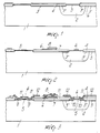
- the process according to the invention initially comprises conventional process steps to manufacture, in a body or substrate 1 of semiconductor material having a first type of conductivity, at least one well 2 with the opposite type of conductivity, by means of an appropriate masking, doping and diffusion step. Said diffusion is normally performed at high temperature (typically 1200°C) in order to manufacture wells with a considerable junction depth able of accommodating transistors.
- a layer of inert material typically silicon nitride
- the nitride is shaped so as to cover only the active regions in which the transistors are to be provided, leaving free the regions in which the insulations and the field oxide are to be provided.
- Doping ions adapted to provide a conductivity equal to that of the regions in which they are implanted are subsequently implanted by means of two masking steps in succession, in order to increase their concentration and form insulation regions (channel stoppers).
- the implantations are performed at appropriate energy levels so that, the various areas covered by the inert material which delimits the active areas are shielded.
- Field oxidation is then performed, leading to the forming of a silicon oxide layer indicated by the reference numeral 4 in figure 1 only in the regions free from the inert material, simultaneously diffusing all the doping ion species present in the structure, forming the insulation regions 3′ in the substrate and 3 ⁇ in the well.
- This oxidation is normally performed at temperatures of approximately 1000°C, the effect of displacing the doping species being especially effective in the insulation regions; these doping agents, contrary to those forming the well, have not yet undergone thermal treatments.
- the process steps leading to the production of the gate electrodes and of the capacitors would entail a masking step to define the gate regions of the transistors and of the lower electrodes of the capacitors, a step of surface thermal oxidation of the polysilicon to form the dielectric of the capacitors, a further deposition of polycrystalline silicon and its doping and shaping in order to delimit the upper plates or the electrodes of the capacitors.
- the thermal oxidation step can lead to a displacement of the doping ion species, producing the already mentioned negative effects.
- a silicon oxide layer is formed at low temperature, specifically by depositing at a temperature such as not to cause a significant displacement of the doping species.
- the silicon oxide is deposited by oxidation in O2 of tetraethylorthosilicate at 700°C. Due to the relatively low temperature of this process it is thus possible to obtain a film or thin layer of silicon oxide, indicated by 7 in figure 2, conveniently acting is dielectric of the capacitors, its manufacturing causing no alterations in the underlying structure.
- the process can thus continue conventionally with a subsequent deposition of a layer of polycrystalline silicon and related doping, so as to form a layer 8 similar to the layer 6, obtaining a "sandwich" formed by two layers of polycrystalline silicon separated by a film or thin layer of silicon oxide.
- a masking step is then conventionally performed on the last layer 8 of the polycrystalline silicon and on the deposited oxide film 7, thus obtaining one of the plates of the capacitors and thus uncovering the surface of the first polysilicon layer 6.
- a subsequent masking of the first polycrystalline silicon layer 6 defines the gate electrodes of the transistors and simultaneously the second plate of the capacitors. The structure illustrated in figure 2 is thus obtained.
- the following process steps comprise two successive masking steps to implant ions in the active areas not covered by polycrystalline silicon to form the source and drain junctions of the transistors.
- the oxide interposed between the two plates of the capacitors is obtained by means of a low-temperature process which causes no displacement of the doping species and therefore does not alter the other structures.
- the process of therefore manufacturing integrated capacitors with low voltage coefficient without altering any of the other structures of the device is extremely advantageous, particularly in view of the development of more advanced processes in which a higher level of integration is required.
- the invention thus conceived is susceptible to numerous modification and variations, all of which are within the scope of the inventive concept.
- the described embodiment merely constitutes one possible manner of implementing the invention in a silicon-gate CMOS process, but other sequences of operations can be performed to obtain the resulting structure.
- the invention is furthermore applicable to capacitors the plates whereof are doped with different methods (such as e.g. by vapors composed of the doping agents for ion implantation or even with other less conventional methods).
- the invention furthermore comprises the variation in which the plates of the capacitors are not both provided by means of an appropriately doped polycrystalline silicon layer but are manufactured e.g. one by means of a polycrystalline silicon layer and the other by the metallic layer (typically aluminum) used for the connections.
- this solution entails a sequence of operations which is thoroughly different from the one described in the example, but is still based on forming by deposition of silicon oxides at low temperature in order to manufacture the dielectric layer of the capacitors. It is obvious that in this case the above mentioned characteristic is even more important, since the dielectric is manufactured at a more advanced stage of the production process, so that the altering influence of said process is higher on the already manufactured structures.
Landscapes
- Semiconductor Integrated Circuits (AREA)
- Metal-Oxide And Bipolar Metal-Oxide Semiconductor Integrated Circuits (AREA)
Applications Claiming Priority (2)
| Application Number | Priority Date | Filing Date | Title |
|---|---|---|---|
| IT8723200A IT1224656B (it) | 1987-12-23 | 1987-12-23 | Procedimento per la fabbricazione di condensatori integrati in tecnologia mos. |
| IT2320087 | 1987-12-23 |
Publications (2)
| Publication Number | Publication Date |
|---|---|
| EP0321860A2 true EP0321860A2 (de) | 1989-06-28 |
| EP0321860A3 EP0321860A3 (de) | 1990-03-07 |
Family
ID=11204822
Family Applications (1)
| Application Number | Title | Priority Date | Filing Date |
|---|---|---|---|
| EP88120975A Ceased EP0321860A3 (de) | 1987-12-23 | 1988-12-15 | Verfahren zum Herstellen integrierter Kondensatoren in MOS-Technik |
Country Status (3)
| Country | Link |
|---|---|
| EP (1) | EP0321860A3 (de) |
| JP (2) | JP2766492B2 (de) |
| IT (1) | IT1224656B (de) |
Cited By (4)
| Publication number | Priority date | Publication date | Assignee | Title |
|---|---|---|---|---|
| EP0443958A1 (de) * | 1990-02-23 | 1991-08-28 | France Telecom | Verfahren zum Herstellen einer analogen integrierten Hochgeschwindigkeitsschaltung unter Verwendung von lokalen Leitungsverbindungen aus Silizid |
| EP0435534A3 (en) * | 1989-12-14 | 1991-11-06 | Sgs-Thomson Microelectronics S.R.L. | Method of manufacturing integrated circuit and integrated circuit made thereby |
| US5851871A (en) * | 1987-12-23 | 1998-12-22 | Sgs-Thomson Microelectronics, S.R.L. | Process for manufacturing integrated capacitors in MOS technology |
| CN115241131A (zh) * | 2022-08-05 | 2022-10-25 | 重庆中科渝芯电子有限公司 | 多层栅模拟cmos工艺边缘应力优化集成方法和低电压系数多晶电容器 |
Families Citing this family (1)
| Publication number | Priority date | Publication date | Assignee | Title |
|---|---|---|---|---|
| KR0167274B1 (ko) * | 1995-12-07 | 1998-12-15 | 문정환 | 씨모스 아날로그 반도체장치와 그 제조방법 |
Family Cites Families (6)
| Publication number | Priority date | Publication date | Assignee | Title |
|---|---|---|---|---|
| US4261772A (en) * | 1979-07-06 | 1981-04-14 | American Microsystems, Inc. | Method for forming voltage-invariant capacitors for MOS type integrated circuit device utilizing oxidation and reflow techniques |
| US4577390A (en) * | 1983-02-23 | 1986-03-25 | Texas Instruments Incorporated | Fabrication of polysilicon to polysilicon capacitors with a composite dielectric layer |
| JPS60113960A (ja) * | 1983-11-25 | 1985-06-20 | Nec Corp | 半導体容量装置 |
| US4639274A (en) * | 1984-11-28 | 1987-01-27 | Fairchild Semiconductor Corporation | Method of making precision high-value MOS capacitors |
| DE3679596D1 (de) * | 1985-05-22 | 1991-07-11 | Siemens Ag | Verfahren zum herstellen von mit bor und phosphor dotierten siliziumoxid-schichten fuer integrierte halbleiterschaltungen. |
| JPS6218042A (ja) * | 1985-06-24 | 1987-01-27 | サ−ムコ・システムス・インコ−ポレ−テツド | 気化された液体反応体からの二酸化ケイ素の低圧化学蒸着法 |
-
1987
- 1987-12-23 IT IT8723200A patent/IT1224656B/it active
-
1988
- 1988-12-15 EP EP88120975A patent/EP0321860A3/de not_active Ceased
- 1988-12-21 JP JP63324719A patent/JP2766492B2/ja not_active Expired - Lifetime
-
1997
- 1997-07-29 JP JP9203590A patent/JPH10144871A/ja active Pending
Cited By (5)
| Publication number | Priority date | Publication date | Assignee | Title |
|---|---|---|---|---|
| US5851871A (en) * | 1987-12-23 | 1998-12-22 | Sgs-Thomson Microelectronics, S.R.L. | Process for manufacturing integrated capacitors in MOS technology |
| EP0435534A3 (en) * | 1989-12-14 | 1991-11-06 | Sgs-Thomson Microelectronics S.R.L. | Method of manufacturing integrated circuit and integrated circuit made thereby |
| EP0443958A1 (de) * | 1990-02-23 | 1991-08-28 | France Telecom | Verfahren zum Herstellen einer analogen integrierten Hochgeschwindigkeitsschaltung unter Verwendung von lokalen Leitungsverbindungen aus Silizid |
| FR2658951A1 (fr) * | 1990-02-23 | 1991-08-30 | Bonis Maurice | Procede de fabrication d'un circuit integre pour filiere analogique rapide utilisant des lignes d'interconnexions locales en siliciure. |
| CN115241131A (zh) * | 2022-08-05 | 2022-10-25 | 重庆中科渝芯电子有限公司 | 多层栅模拟cmos工艺边缘应力优化集成方法和低电压系数多晶电容器 |
Also Published As
| Publication number | Publication date |
|---|---|
| JPH10144871A (ja) | 1998-05-29 |
| IT8723200A0 (it) | 1987-12-23 |
| JP2766492B2 (ja) | 1998-06-18 |
| IT1224656B (it) | 1990-10-18 |
| JPH02138769A (ja) | 1990-05-28 |
| EP0321860A3 (de) | 1990-03-07 |
Similar Documents
| Publication | Publication Date | Title |
|---|---|---|
| US4422885A (en) | Polysilicon-doped-first CMOS process | |
| US4319395A (en) | Method of making self-aligned device | |
| US4199773A (en) | Insulated gate field effect silicon-on-sapphire transistor and method of making same | |
| US6043157A (en) | Semiconductor device having dual gate electrode material and process of fabrication thereof | |
| US4183040A (en) | MOS RAM with implant forming peripheral depletion MOSFET channels and capacitor bottom electrodes | |
| KR100304678B1 (ko) | 배선을형성한후에수소이온으로문턱전압을변경시키는것이가능한전계효과트랜지스터를구비한반도체장치제조방법 | |
| US5397715A (en) | MOS transistor having increased gate-drain capacitance | |
| US4045250A (en) | Method of making a semiconductor device | |
| KR100420870B1 (ko) | Eeprom-반도체구조물의제조방법 | |
| US4639274A (en) | Method of making precision high-value MOS capacitors | |
| EP0135243B1 (de) | Verfahren zum Herstellen einer Halbleiterstruktur auf einem Substrat und danach hergestellte Halbleiteranordnung | |
| US3463974A (en) | Mos transistor and method of manufacture | |
| KR0179360B1 (ko) | 유전물질에 의해 분리되어 있는 전극쌍이 포함된 다양한 소자를 구비한 집적회로의 제조방법 | |
| US5494843A (en) | Method for forming MOSFET devices | |
| CA1237537A (en) | Method of making mosfets using silicate glass layer as gate edge masking for ion implantation | |
| US5153146A (en) | Maufacturing method of semiconductor devices | |
| US4081896A (en) | Method of making a substrate contact for an integrated circuit | |
| US6117739A (en) | Semiconductor device with layered doped regions and methods of manufacture | |
| EP0337481B1 (de) | Halbleitervorrichtung | |
| KR100367740B1 (ko) | 반도체 소자의 게이트 산화막 제조방법 | |
| JP4872395B2 (ja) | シリコン酸化膜形成法、容量素子の製法及び半導体装置の製法 | |
| EP0321860A2 (de) | Verfahren zum Herstellen integrierter Kondensatoren in MOS-Technik | |
| US4826779A (en) | Integrated capacitor and method of fabricating same | |
| US4218267A (en) | Microelectronic fabrication method minimizing threshold voltage variation | |
| KR20020047230A (ko) | 반사-방지 코팅으로 반도체 메모리 디바이스를 제조하는방법 |
Legal Events
| Date | Code | Title | Description |
|---|---|---|---|
| PUAI | Public reference made under article 153(3) epc to a published international application that has entered the european phase |
Free format text: ORIGINAL CODE: 0009012 |
|
| AK | Designated contracting states |
Kind code of ref document: A2 Designated state(s): DE FR GB NL SE |
|
| PUAL | Search report despatched |
Free format text: ORIGINAL CODE: 0009013 |
|
| AK | Designated contracting states |
Kind code of ref document: A3 Designated state(s): DE FR GB NL SE |
|
| 17P | Request for examination filed |
Effective date: 19900322 |
|
| 17Q | First examination report despatched |
Effective date: 19920529 |
|
| APAB | Appeal dossier modified |
Free format text: ORIGINAL CODE: EPIDOS NOAPE |
|
| STAA | Information on the status of an ep patent application or granted ep patent |
Free format text: STATUS: THE APPLICATION HAS BEEN REFUSED |
|
| 18R | Application refused |
Effective date: 19970314 |
|
| APAF | Appeal reference modified |
Free format text: ORIGINAL CODE: EPIDOSCREFNE |