EP0322577A2 - Signal delay circuit - Google Patents
Signal delay circuit Download PDFInfo
- Publication number
- EP0322577A2 EP0322577A2 EP88119927A EP88119927A EP0322577A2 EP 0322577 A2 EP0322577 A2 EP 0322577A2 EP 88119927 A EP88119927 A EP 88119927A EP 88119927 A EP88119927 A EP 88119927A EP 0322577 A2 EP0322577 A2 EP 0322577A2
- Authority
- EP
- European Patent Office
- Prior art keywords
- transistors
- circuit
- delay circuit
- inverter
- input
- Prior art date
- Legal status (The legal status is an assumption and is not a legal conclusion. Google has not performed a legal analysis and makes no representation as to the accuracy of the status listed.)
- Granted
Links
Images
Classifications
-
- H—ELECTRICITY
- H03—ELECTRONIC CIRCUITRY
- H03K—PULSE TECHNIQUE
- H03K5/00—Manipulating of pulses not covered by one of the other main groups of this subclass
- H03K5/13—Arrangements having a single output and transforming input signals into pulses delivered at desired time intervals
- H03K5/133—Arrangements having a single output and transforming input signals into pulses delivered at desired time intervals using a chain of active delay devices
-
- H—ELECTRICITY
- H10—SEMICONDUCTOR DEVICES; ELECTRIC SOLID-STATE DEVICES NOT OTHERWISE PROVIDED FOR
- H10D—INORGANIC ELECTRIC SEMICONDUCTOR DEVICES
- H10D84/00—Integrated devices formed in or on semiconductor substrates that comprise only semiconducting layers, e.g. on Si wafers or on GaAs-on-Si wafers
- H10D84/80—Integrated devices formed in or on semiconductor substrates that comprise only semiconducting layers, e.g. on Si wafers or on GaAs-on-Si wafers characterised by the integration of at least one component covered by groups H10D12/00 or H10D30/00, e.g. integration of IGFETs
- H10D84/82—Integrated devices formed in or on semiconductor substrates that comprise only semiconducting layers, e.g. on Si wafers or on GaAs-on-Si wafers characterised by the integration of at least one component covered by groups H10D12/00 or H10D30/00, e.g. integration of IGFETs of only field-effect components
- H10D84/83—Integrated devices formed in or on semiconductor substrates that comprise only semiconducting layers, e.g. on Si wafers or on GaAs-on-Si wafers characterised by the integration of at least one component covered by groups H10D12/00 or H10D30/00, e.g. integration of IGFETs of only field-effect components of only insulated-gate FETs [IGFET]
- H10D84/85—Complementary IGFETs, e.g. CMOS
-
- H—ELECTRICITY
- H03—ELECTRONIC CIRCUITRY
- H03K—PULSE TECHNIQUE
- H03K5/00—Manipulating of pulses not covered by one of the other main groups of this subclass
- H03K2005/00013—Delay, i.e. output pulse is delayed after input pulse and pulse length of output pulse is dependent on pulse length of input pulse
- H03K2005/0015—Layout of the delay element
- H03K2005/00195—Layout of the delay element using FET's
-
- H—ELECTRICITY
- H03—ELECTRONIC CIRCUITRY
- H03K—PULSE TECHNIQUE
- H03K5/00—Manipulating of pulses not covered by one of the other main groups of this subclass
- H03K2005/00013—Delay, i.e. output pulse is delayed after input pulse and pulse length of output pulse is dependent on pulse length of input pulse
- H03K2005/0015—Layout of the delay element
- H03K2005/00195—Layout of the delay element using FET's
- H03K2005/00215—Layout of the delay element using FET's where the conduction path of multiple FET's is in parallel or in series, all having the same gate control
Definitions
- This invention relates to a signal delay circuit and, more particularly, to a complementary metal oxide semiconductor (CMOS) field effect transistor FET delay circuit of the integrated circuit type which may be formed in a semiconductor substrate, such as silicon.
- CMOS complementary metal oxide semiconductor
- circuits for producing signal delay are well known in the prior art.
- One known type of signal delay circuit is the basic resistor-capacitor or RC circuit. This type of delay circuit is disclosed in, e.g., U.S. Patent 4,430,587, filed January 13, 1982, entitled “MOS FIXED DELAY CIRCUIT", and U.S. Patent 4,516,312, filed February 10, 1982, entitled “METHOD FOR CONSTRUCTING DELAY CIRCUITS IN A MASTER SLICE IC”.
- Another known type of delay circuit is implemented by an inverter or a series of inverters as disclosed in, e.g., U.S.
- Patent 4,476,401 filed January 31, 1983, entitled “WRITE STROBE GENERATOR FOR CLOCK SYNCHRONIZED MEMORY”
- U.S. Patent 4,700,089 filed August 20, 1985, entitled “DELAY CIRCUIT FOR GATE-ARRAY LSI”.
- a further known type of delay circuit is disclosed in U.S. Patent 4,388,538, filed September 29, 1980, entitled “DELAY SIGNAL GENERATING CIRCUIT”, which is implemented in N-channel field effect transistor or NMOS technology and which uses a bootstrap operation and depletion devices.
- Patent 4,511,814 filed November 29, 1982, entitled “SEMICONDUCTOR ANALOG SWITCH CIRCUIT WITH COMPENSATION MEANS TO MINIMIZE OFFSET OF CIRCUIT VOLTAGE", discloses a circuit having a pass gate or, more particularly, parallelly connected CMOS transistors, through which signals pass from an input terminal to an output terminal.
- the invention as claimed solves the problem of providing an improved signal delay circuit which uses minimal surface area on a semiconductor substrate or chip and minimal power, yet which is expandable for selectable and various amounts of time delays, while reducing testability concerns.
- a delay circuit which includes first and second circuits connected in parallel with each other.
- the first circuit includes serially connected first and second transistors of a first conductivity type
- the second circuit includes serially connected third and fourth transistors of a conductivity type opposite to the first one.
- a fifth transistor of the first conductivity type and a sixth one of the opposite conductivity type are connected in parallel from the common point provided between the first and second transistors to the common point between the third and fourth transistors.
- a signal to be delayed is applied to one end of the parallely arranged first and second circuits, and a complementary signal to the control electrodes of the transistors.
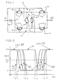
- FIG. 1 of the drawings there is shown a circuit diagram of a preferred embodiment of the CMOS FET delay circuit of the present invention.
- the circuit being made in the CMOS technology, has its P-channel field effect transistors indicated by a rectangle with a diagonal line formed therein and a gate electrode arranged adjacent thereto and its N-channel field effect transistors indicated by a rectangle without a diagonal line and a gate electrode arranged adjacent thereto.
- the CMOS FET delay circuit of the present invention illustrated in FIG. 1 includes a first series circuit 10 having first and second field effect transistors 12 and 14, respectively, of the P-channel type connected between a first node A and an output terminal OUT and a second series circuit 16 having third and fourth field effect transistors 18 and 20, respectively, of the N-channel type connected between the first node A and the output terminal OUT.
- a second node B is located at the common point between the third and fourth N-channel transistors 18 and 20 and a third node C is located at the common point between the first and second transistors 12 and 14.
- a fifth field effect transistor 22 of the P-channel type is connected between node B and node C, and a sixth field effect transistor 24 of the N-channel type is also connected between node B and node C.
- P-type diffusions are indicated by P for the source/drain regions of the P-channel transistors 12, 14 and 22, and N-type diffusions, preferably N+, are indicated by N for the source/drain regions of the N-channel transistors 18, 20 and 24, which will be discussed in more detail hereinbelow.
- An input terminal IN is provided for receiving an input signal such as a binary logic signal which is connected to each of the control electrodes of the transistors 12, 14, 18, 20, 22 and 24.
- An inverter 26 of preferably any known CMOS type is connected between the input terminal IN and the first node A.
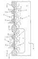
- FIG. 2 of the drawings there is illustrated a cross-sectional view of the P-channel transistors 12 and 14 and the N-channel transistors 18 and 20 shown in FIG. 1 taken through a silicon substrate 28 having a P-type conductivity. Elements in FIG. 2 which are similar to corresponding elements in FIG. 1 are provided with the same reference characters.
- the substrate 28 includes an N-well 30 with a thin layer of silicon dioxide 32 formed on the surface thereof. Recessed oxide regions ROX are disposed at the edges of the N-well to electrically isolate the N-well from the remainder of the substrate, as is well known.
- the first and second P-channel transistors 12 and 14 are formed in the N-well 30.
- Transistor 12 includes the P-type diffusions P of the source/drain regions forming capacitive or P-N junctions with the N-type conductivity N-well 30 identified as capacitors C1 and C2, and transistor 14 includes the P-type diffusions P of the source/drain regions forming capacitive or P-N junctions with the N-type conductivity N-well 30 identified as capacitor C3 and the capacitor C2, which is common to both transistors 12 and 14.
- Control or gate electrodes for the transistors 12 and 14 are indicated at G.
- the impurity used for the P-type diffusions may be boron.
- the N-channel transistors 18 and 20 are formed at the surface of the substrate 28 outside of the N-well 30.
- the transistor 18 includes the N-type diffusions N ' of the source/drain regions forming capacitive or P-N junctions with the P-type conductivity silicon substrate 28 identified as capacitors C4 and C5, and transistor 20 includes the N-type diffusions N of the source/drain regions forming capacitive or P-N junctions with the P-type conductivity silicon substrate 28 identified as capacitor C6 and the capacitor C5, which is common to both transistors 18 and 20.
- Control or gate electrodes for the transistors 18 and 20 are indicated at G.
- the impurity used for the N-type diffusions may be arsenic or phosphorous.
- the region below the gate electrodes at the surface of the semiconductor substrate between the source/drain regions of the transistors 12, 14, 18 and 20 is the channel region which when inverted permits electrical conduction between the node A and the terminal OUT ⁇ .
- the voltage at the output of the inverter 26 i.e., at node A
- the voltage at node B also begins to fall due to the turn on of the transistor 18.
- the N-channel transistors 20 and 24 turn on to drop the voltage at the output terminal OOT and at node C, as indicated in FIG. 3.
- the voltage at the output terminal OUT falls to Vdd/2, with the delay in the signal from the input terminal IN to the output terminal OUT being equal to time t 2 minus time ti.
- the voltage at the output terminal OUT thereafter falls to 0 volts at time t a , with the voltage at the input terminal IN being at Vdd volts.
- the voltage at the input terminal IN is lowered toward 0 volts, with the input voltage being at Vdd/2 at time ts.
- the voltage at node A begins to rise due to the charge received from the inverter 26.
- the P-channel transistor 12 With the rise of the voltage at node A and the fall of the voltage at the input terminal IN, the P-channel transistor 12 turns on to begin charging up node C.
- P-channel transistors 14 and 22 turn on to begin charging the output terminal OUT and the node B.
- the voltage at the output terminal reaches a value of Vdd/2 and at time t 7 the output voltage is the full power supply voltage of Vdd volts.
- the voltage at node B could rise sooner or later than that of the output terminal OUT, or simultaneously therewith.
- the voltage at node C could fall sooner or later than that of the output terminal OUT between the times t, and t a .
- the fall delay and the rise delay of the output voltage may, if desired, be made unequal by merely altering the characteristics of the transistors in the two different paths, i.e., the RC time constant produced by resistive path R1 and capacitors C1, C2 and C3 in the series circuit which includes P-channel transistors 12 and 14 may be made different from the RC time constant produced by resistive path R2 and capacitors C4, C5 and C6 in the series circuit which includes N-channel transistors 18 and 20.
- the addition of the P-channel transistor 22 and the N-channel transistor 24 significantly increases the capacitance of the two paths between the node A and the output terminal OUT by adding the capacitance at node B and node C, respectively.
- node C and node B are reset to insure maximum delay at the next transition of the signal.
- the capacitance values of the capacitors of the circuit such as capacitors C1, C2, C3, C4, C5 and C6, and the resistance values of resistors R1 and R2 may be altered by using various impurities as well as different concentrations thereof in the substrate, especially in the source / drain regions, or by . altering the sizes of the various elements in the circuit, e.g., using different beta ratios, i.e., transistor channel width to length ratios.
- the rising delay of the signal, or voltage at the output terminal may be made longer or shorter than that of the falling delay, or they may be made equal to each other, i.e., the rising delay, time t 6 minus time ts, may be equal to the falling delay, time t 2 minus time ti, taken at the voltage level VddI2, the effective switch point of the transistors, as indicated in FIG. 3 of the drawings.
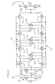
- the signal delay circuit of FIG. 4 includes a first series circuit having the P-channel transistors 12 and 14 and added P-channel transistors 12 and 14 connected between the node A and the output terminal OUT and a second series circuit having the N-channel transistors 18 and 20 and added N-channel transistors 18 and 20 also connected between the node A and the output terminal OUT.
- Node B' is located at the common point between the N-channel transistors 20 and 18 and node B" is located at the common point between N-channel transistors 18 and 20'.
- Node C' is located at the common point between P-channel transistors 14 and 12 and node C is located at the common point between transistors 12 and 14.
- a P-channel transistor 22 is connected between nodes B' and C and an N-channel transistor 24 is also connected between nodes B and C'.
- a P-channel transistor 22 is connected between nodes B and C and an N-channel transistor 24 is also connected between nodes B and C".
- the signal delay circuit of FIG. 4 also includes a second inverter 26 having an input connected to the node A and an output connected to a terminal IN which is connected to the control or gate electrodes of each of the transistors connected between the node A and the output terminal OUT. A higher driving voltage is provided by connecting these control electrodes to the output of the second inverter 26 than to the input terminal IN.
- a third inverter 26 having an input connected to the output terminal OUT and an output connected to an output terminal OUT is provided to produce a non-inverted output signal. It should be understood that additional stages of delay in accordance with the teaching of this invention may be inserted between the node A and the output terminal OUT if even longer delay times are required.
- the circuit of FIG. 4 operates in the same manner as that of FIG. 1 except that additional stages have been provided to increase the RC time constant of the circuit.
- the signal delay circuit of the present invention provides an output voltage which swings between full supply voltage Vdd and ground in view of the use of the P-channel transistors for charging the output terminal OUT and the use of the N-channel transistors for discharging the output terminal OUT.
- a signal delay circuit which requires only one inverter and, therefore, uses minimal switching power, up to 50% less power per unit delay, and which can be made within a very small surface area of the semiconductor substrate per nanosecond of delay due to the arrangement of the CMOS transistors in the circuit, up to two times more delay pre unit area.
- the delay circuit which is very useful in an automated design environment, is readily . expandable to provide desired delay periods, while reducing testability concerns since only one path, i.e., the N-channel device path or the P-channel device path, conducts in a cycle to more readily detect fault mechanisms.
- this delay circuit provides flexible implementation of asymmetric delay between the rise delay and fall delay of the input signal.
Landscapes
- Physics & Mathematics (AREA)
- Nonlinear Science (AREA)
- Pulse Circuits (AREA)
- Metal-Oxide And Bipolar Metal-Oxide Semiconductor Integrated Circuits (AREA)
- Networks Using Active Elements (AREA)
Abstract
Description
- This invention relates to a signal delay circuit and, more particularly, to a complementary metal oxide semiconductor (CMOS) field effect transistor FET delay circuit of the integrated circuit type which may be formed in a semiconductor substrate, such as silicon.
- At times it is desired to delay signals, such as binary logic signals, for timing considerations, such as race conditions caused by high speed circuits or paths, skewing of off-chip driver switching to reduce power bus noise, or other such reasons.
- Circuits for producing signal delay are well known in the prior art. One known type of signal delay circuit is the basic resistor-capacitor or RC circuit. This type of delay circuit is disclosed in, e.g., U.S. Patent 4,430,587, filed January 13, 1982, entitled "MOS FIXED DELAY CIRCUIT", and U.S. Patent 4,516,312, filed February 10, 1982, entitled "METHOD FOR CONSTRUCTING DELAY CIRCUITS IN A MASTER SLICE IC". Another known type of delay circuit is implemented by an inverter or a series of inverters as disclosed in, e.g., U.S. Patent 4,476,401, filed January 31, 1983, entitled "WRITE STROBE GENERATOR FOR CLOCK SYNCHRONIZED MEMORY", and U.S. Patent 4,700,089, filed August 20, 1985, entitled "DELAY CIRCUIT FOR GATE-ARRAY LSI". A further known type of delay circuit is disclosed in U.S. Patent 4,388,538, filed September 29, 1980, entitled "DELAY SIGNAL GENERATING CIRCUIT", which is implemented in N-channel field effect transistor or NMOS technology and which uses a bootstrap operation and depletion devices. Although not designed as a signal delay circuit, U.S. Patent 4,511,814, filed November 29, 1982, entitled "SEMICONDUCTOR ANALOG SWITCH CIRCUIT WITH COMPENSATION MEANS TO MINIMIZE OFFSET OF CIRCUIT VOLTAGE", discloses a circuit having a pass gate or, more particularly, parallelly connected CMOS transistors, through which signals pass from an input terminal to an output terminal.
- The invention as claimed solves the problem of providing an improved signal delay circuit which uses minimal surface area on a semiconductor substrate or chip and minimal power, yet which is expandable for selectable and various amounts of time delays, while reducing testability concerns.
- The advantages offered by the invention are achieved by a delay circuit which includes first and second circuits connected in parallel with each other. The first circuit includes serially connected first and second transistors of a first conductivity type, and the second circuit includes serially connected third and fourth transistors of a conductivity type opposite to the first one. A fifth transistor of the first conductivity type and a sixth one of the opposite conductivity type are connected in parallel from the common point provided between the first and second transistors to the common point between the third and fourth transistors. A signal to be delayed is applied to one end of the parallely arranged first and second circuits, and a complementary signal to the control electrodes of the transistors.
- The invention is described in detail below with reference to the drawings in which:
- FIG. 1 is a circuit diagram of a preferred embodiment of the present invention,
- FIG. 2 illustrates a cross-sectional view taken through a silicon substrate of a first series circuit of P-channel transistors and of a second series circuit of N-channel transistors used in the circuit of FIG. 1,
- FIG. 3 is a pulse program of the voltages at various points or nodes in the circuit of FIG. 1 plotted against time, and
- FIG. 4 is a circuit diagram similar to that of FIG. 1 but with additional buffers and stages which provides an expanded non-inverted output signal delay.
- Referring to FIG. 1 of the drawings in more detail, there is shown a circuit diagram of a preferred embodiment of the CMOS FET delay circuit of the present invention. The circuit, being made in the CMOS technology, has its P-channel field effect transistors indicated by a rectangle with a diagonal line formed therein and a gate electrode arranged adjacent thereto and its N-channel field effect transistors indicated by a rectangle without a diagonal line and a gate electrode arranged adjacent thereto.
- The CMOS FET delay circuit of the present invention illustrated in FIG. 1 includes a
first series circuit 10 having first and secondfield effect transistors second series circuit 16 having third and fourthfield effect transistors channel transistors second transistors field effect transistor 22 of the P-channel type is connected between node B and node C, and a sixthfield effect transistor 24 of the N-channel type is also connected between node B and node C. - P-type diffusions, preferably P+, are indicated by P for the source/drain regions of the P-
channel transistors channel transistors - An input terminal IN is provided for receiving an input signal such as a binary logic signal which is connected to each of the control electrodes of the
transistors inverter 26 of preferably any known CMOS type is connected between the input terminal IN and the first node A. - In FIG. 2 of the drawings there is illustrated a cross-sectional view of the P-
channel transistors channel transistors silicon substrate 28 having a P-type conductivity. Elements in FIG. 2 which are similar to corresponding elements in FIG. 1 are provided with the same reference characters. As shown in FIG. 2 thesubstrate 28 includes an N-well 30 with a thin layer ofsilicon dioxide 32 formed on the surface thereof. Recessed oxide regions ROX are disposed at the edges of the N-well to electrically isolate the N-well from the remainder of the substrate, as is well known. As can be seen in FIG. 2, the first and second P-channel transistors Transistor 12 includes the P-type diffusions P of the source/drain regions forming capacitive or P-N junctions with the N-type conductivity N-well 30 identified as capacitors C1 and C2, andtransistor 14 includes the P-type diffusions P of the source/drain regions forming capacitive or P-N junctions with the N-type conductivity N-well 30 identified as capacitor C3 and the capacitor C2, which is common to bothtransistors transistors - The N-
channel transistors substrate 28 outside of the N-well 30. Thetransistor 18 includes the N-type diffusions N 'of the source/drain regions forming capacitive or P-N junctions with the P-typeconductivity silicon substrate 28 identified as capacitors C4 and C5, andtransistor 20 includes the N-type diffusions N of the source/drain regions forming capacitive or P-N junctions with the P-typeconductivity silicon substrate 28 identified as capacitor C6 and the capacitor C5, which is common to bothtransistors transistors - As is also known, the region below the gate electrodes at the surface of the semiconductor substrate between the source/drain regions of the
transistors channel transistors channel transistors channel transistors channel transistors - In order to better understand the operation of the invention, reference may be had to the pulse program shown in FIG. 3 of the drawings along with the circuit diagram of FIG. 1 and the cross-sectional view of FIG. 2. As can be seen from the graph of FIG. 3, wherein voltage is plotted against time at the input terminal IN, the output terminal 6UT and the nodes A,B and C, when the voltage at terminal IN is at 0 volts, the voltage at the nodes A, B and C and at terminal OUT is at Vdd or 5 volts, since each of these points of the delay circuit are connected to the output of the
inverter 26. At time to, the voltage begins to rise toward Vdd and when at time t, it reaches Vdd/2, the approximate switch point of theinverter 26, the voltage at the output of theinverter 26, i.e., at node A, will begin to fall due to the discharge of node A through theinverter 26. Since the voltage at node A is falling and the voltage at the control electrodes of the N-channel transistors transistor 18. With the voltage at node B continuing to fall and the voltage at the input terminal IN continuing to rise, the N-channel transistors - At time t4, the voltage at the input terminal IN is lowered toward 0 volts, with the input voltage being at Vdd/2 at time ts. At time ts, the voltage at node A begins to rise due to the charge received from the
inverter 26. With the rise of the voltage at node A and the fall of the voltage at the input terminal IN, the P-channel transistor 12 turns on to begin charging up node C. With charge accumulating on node C, P-channel transistors - It should be noted that depending upon the characteristics of the circuit, especially of the P-
channel transistors channel transistors channel transistors channel transistors channel transistor 22 and the N-channel transistor 24 significantly increases the capacitance of the two paths between the node A and the output terminal OUT by adding the capacitance at node B and node C, respectively. Furthermore, by usingtransistors - To provide a non-inverting delay circuit in accordance with the teachings of this invention as well as a longer delay period, the embodiment illustrated in FIG. 4 may be used. In the circuit of FIG. 4 elements similar to those of the circuit of FIG. 1 have been identified with the same reference characters. The signal delay circuit of FIG. 4 . includes a first series circuit having the P-
channel transistors channel transistors channel transistors channel transistors channel transistors channel transistors 18 and 20'. Node C' is located at the common point between P-channel transistors transistors channel transistor 22 is connected between nodes B' and C and an N-channel transistor 24 is also connected between nodes B and C'. - A P-
channel transistor 22 is connected between nodes B and C and an N-channel transistor 24 is also connected between nodes B and C". - The signal delay circuit of FIG. 4 also includes a
second inverter 26 having an input connected to the node A and an output connected to a terminal IN which is connected to the control or gate electrodes of each of the transistors connected between the node A and the output terminal OUT. A higher driving voltage is provided by connecting these control electrodes to the output of thesecond inverter 26 than to the input terminal IN. Athird inverter 26 having an input connected to the output terminal OUT and an output connected to an output terminal OUT is provided to produce a non-inverted output signal. It should be understood that additional stages of delay in accordance with the teaching of this invention may be inserted between the node A and the output terminal OUT if even longer delay times are required. - The circuit of FIG. 4 operates in the same manner as that of FIG. 1 except that additional stages have been provided to increase the RC time constant of the circuit.
- It should be noted that the signal delay circuit of the present invention provides an output voltage which swings between full supply voltage Vdd and ground in view of the use of the P-channel transistors for charging the output terminal OUT and the use of the N-channel transistors for discharging the output terminal OUT.
- It can be seen that a signal delay circuit has been disclosed which requires only one inverter and, therefore, uses minimal switching power, up to 50% less power per unit delay, and which can be made within a very small surface area of the semiconductor substrate per nanosecond of delay due to the arrangement of the CMOS transistors in the circuit, up to two times more delay pre unit area. Furthermore, the delay circuit, which is very useful in an automated design environment, is readily . expandable to provide desired delay periods, while reducing testability concerns since only one path, i.e., the N-channel device path or the P-channel device path, conducts in a cycle to more readily detect fault mechanisms. Also, this delay circuit provides flexible implementation of asymmetric delay between the rise delay and fall delay of the input signal.
Claims (10)
Applications Claiming Priority (2)
| Application Number | Priority Date | Filing Date | Title |
|---|---|---|---|
| US07/139,551 US4812688A (en) | 1987-12-30 | 1987-12-30 | Transistor delay circuits |
| US139551 | 2002-05-06 |
Publications (3)
| Publication Number | Publication Date |
|---|---|
| EP0322577A2 true EP0322577A2 (en) | 1989-07-05 |
| EP0322577A3 EP0322577A3 (en) | 1989-11-02 |
| EP0322577B1 EP0322577B1 (en) | 1993-06-16 |
Family
ID=22487223
Family Applications (1)
| Application Number | Title | Priority Date | Filing Date |
|---|---|---|---|
| EP88119927A Expired - Lifetime EP0322577B1 (en) | 1987-12-30 | 1988-11-30 | Signal delay circuit |
Country Status (4)
| Country | Link |
|---|---|
| US (1) | US4812688A (en) |
| EP (1) | EP0322577B1 (en) |
| JP (1) | JPH0654864B2 (en) |
| DE (1) | DE3881855T2 (en) |
Families Citing this family (23)
| Publication number | Priority date | Publication date | Assignee | Title |
|---|---|---|---|---|
| US4926074A (en) * | 1987-10-30 | 1990-05-15 | North American Philips Corporation | Semiconductor switch with parallel lateral double diffused MOS transistor and lateral insulated gate transistor |
| US4897563A (en) * | 1988-08-01 | 1990-01-30 | Itt Corporation | N-way MMIC redundant switch |
| US9230910B2 (en) | 2006-03-09 | 2016-01-05 | Tela Innovations, Inc. | Oversized contacts and vias in layout defined by linearly constrained topology |
| US9009641B2 (en) | 2006-03-09 | 2015-04-14 | Tela Innovations, Inc. | Circuits with linear finfet structures |
| US8658542B2 (en) | 2006-03-09 | 2014-02-25 | Tela Innovations, Inc. | Coarse grid design methods and structures |
| US7446352B2 (en) | 2006-03-09 | 2008-11-04 | Tela Innovations, Inc. | Dynamic array architecture |
| US8448102B2 (en) | 2006-03-09 | 2013-05-21 | Tela Innovations, Inc. | Optimizing layout of irregular structures in regular layout context |
| US9563733B2 (en) | 2009-05-06 | 2017-02-07 | Tela Innovations, Inc. | Cell circuit and layout with linear finfet structures |
| US8541879B2 (en) | 2007-12-13 | 2013-09-24 | Tela Innovations, Inc. | Super-self-aligned contacts and method for making the same |
| US7763534B2 (en) | 2007-10-26 | 2010-07-27 | Tela Innovations, Inc. | Methods, structures and designs for self-aligning local interconnects used in integrated circuits |
| US8653857B2 (en) | 2006-03-09 | 2014-02-18 | Tela Innovations, Inc. | Circuitry and layouts for XOR and XNOR logic |
| US8839175B2 (en) | 2006-03-09 | 2014-09-16 | Tela Innovations, Inc. | Scalable meta-data objects |
| US9035359B2 (en) | 2006-03-09 | 2015-05-19 | Tela Innovations, Inc. | Semiconductor chip including region including linear-shaped conductive structures forming gate electrodes and having electrical connection areas arranged relative to inner region between transistors of different types and associated methods |
| US7956421B2 (en) * | 2008-03-13 | 2011-06-07 | Tela Innovations, Inc. | Cross-coupled transistor layouts in restricted gate level layout architecture |
| US7908578B2 (en) | 2007-08-02 | 2011-03-15 | Tela Innovations, Inc. | Methods for designing semiconductor device with dynamic array section |
| US8667443B2 (en) | 2007-03-05 | 2014-03-04 | Tela Innovations, Inc. | Integrated circuit cell library for multiple patterning |
| US8453094B2 (en) | 2008-01-31 | 2013-05-28 | Tela Innovations, Inc. | Enforcement of semiconductor structure regularity for localized transistors and interconnect |
| US7939443B2 (en) | 2008-03-27 | 2011-05-10 | Tela Innovations, Inc. | Methods for multi-wire routing and apparatus implementing same |
| KR101761530B1 (en) | 2008-07-16 | 2017-07-25 | 텔라 이노베이션스, 인코포레이티드 | Methods for cell phasing and placement in dynamic array architecture and implementation of the same |
| US9122832B2 (en) | 2008-08-01 | 2015-09-01 | Tela Innovations, Inc. | Methods for controlling microloading variation in semiconductor wafer layout and fabrication |
| US8661392B2 (en) | 2009-10-13 | 2014-02-25 | Tela Innovations, Inc. | Methods for cell boundary encroachment and layouts implementing the Same |
| US9159627B2 (en) | 2010-11-12 | 2015-10-13 | Tela Innovations, Inc. | Methods for linewidth modification and apparatus implementing the same |
| US11683029B1 (en) * | 2022-01-18 | 2023-06-20 | Nxp B.V. | Charge injection protection devices and methods for input/output interfaces |
Family Cites Families (12)
| Publication number | Priority date | Publication date | Assignee | Title |
|---|---|---|---|---|
| US3986043A (en) * | 1974-12-20 | 1976-10-12 | International Business Machines Corporation | CMOS digital circuits with active shunt feedback amplifier |
| JPS5648715A (en) * | 1979-09-28 | 1981-05-02 | Nec Corp | Delay signal generating circuit |
| JPS5772429A (en) * | 1980-10-22 | 1982-05-06 | Toshiba Corp | Semiconductor integrated circuit device |
| JPS57133712A (en) * | 1981-02-12 | 1982-08-18 | Fujitsu Ltd | Constituting method of delay circuit in master slice ic |
| JPS5894232A (en) * | 1981-11-30 | 1983-06-04 | Toshiba Corp | Semiconductor analog switch circuit |
| US4430587A (en) * | 1982-01-13 | 1984-02-07 | Rockwell International Corporation | MOS Fixed delay circuit |
| JPS58184822A (en) * | 1982-03-31 | 1983-10-28 | Fujitsu Ltd | Input circuit |
| US4473761A (en) * | 1982-04-23 | 1984-09-25 | Motorola, Inc. | Solid state transmission gate |
| US4476401A (en) * | 1983-01-31 | 1984-10-09 | Motorola, Inc. | Write strobe generator for clock synchronized memory |
| US4508983A (en) * | 1983-02-10 | 1985-04-02 | Motorola, Inc. | MOS Analog switch driven by complementary, minimally skewed clock signals |
| US4700089A (en) * | 1984-08-23 | 1987-10-13 | Fujitsu Limited | Delay circuit for gate-array LSI |
| US4694205A (en) * | 1985-06-03 | 1987-09-15 | Advanced Micro Devices, Inc. | Midpoint sense amplification scheme for a CMOS DRAM |
-
1987
- 1987-12-30 US US07/139,551 patent/US4812688A/en not_active Expired - Fee Related
-
1988
- 1988-11-30 DE DE88119927T patent/DE3881855T2/en not_active Expired - Fee Related
- 1988-11-30 EP EP88119927A patent/EP0322577B1/en not_active Expired - Lifetime
- 1988-12-19 JP JP63318673A patent/JPH0654864B2/en not_active Expired - Lifetime
Also Published As
| Publication number | Publication date |
|---|---|
| EP0322577A3 (en) | 1989-11-02 |
| US4812688A (en) | 1989-03-14 |
| DE3881855T2 (en) | 1993-12-23 |
| DE3881855D1 (en) | 1993-07-22 |
| EP0322577B1 (en) | 1993-06-16 |
| JPH01206722A (en) | 1989-08-18 |
| JPH0654864B2 (en) | 1994-07-20 |
Similar Documents
| Publication | Publication Date | Title |
|---|---|---|
| EP0322577B1 (en) | Signal delay circuit | |
| US5767719A (en) | Delay circuit using capacitor and transistor | |
| US4947064A (en) | Semiconductor device having a time delay function | |
| US4617482A (en) | Complementary type MOS field-effect transistor circuit provided with a gate protection structure of small time constant | |
| JPH11177398A (en) | Delay circuit | |
| JPH064181A (en) | Power-on reset signal generator | |
| JPH0454721A (en) | Clock driver circuit | |
| JP3586612B2 (en) | Delay circuit | |
| KR900005792B1 (en) | Control purlse generator | |
| JP3247128B2 (en) | Variable delay circuit | |
| US3638047A (en) | Delay and controlled pulse-generating circuit | |
| US20030189452A1 (en) | Delay circuit and semiconductor device using the same | |
| JPH0152906B2 (en) | ||
| US20010015656A1 (en) | Buffer circuit | |
| US4025800A (en) | Binary frequency divider | |
| US4670672A (en) | C-MOS logic circuit supplied with narrow width pulses converted from input pulses | |
| US5146109A (en) | Circuit for driving a floating circuit in response to a digital signal | |
| JPH01240013A (en) | Semiconductor integrated circuit device | |
| JPH07298607A (en) | Semiconductor booster circuit | |
| JPS6143799B2 (en) | ||
| US4503345A (en) | MOS/LSI Time delay circuit | |
| US3502909A (en) | Pulsed substrate transistor inverter | |
| CN1114268C (en) | Steep edge time-delay relay | |
| KR950008449B1 (en) | Output unit of semiconductor integrated circuit for preventing voltage level variation of semiconductor substrate | |
| EP0856893B1 (en) | Structure and device for selecting design options in an integrated circuit |
Legal Events
| Date | Code | Title | Description |
|---|---|---|---|
| PUAI | Public reference made under article 153(3) epc to a published international application that has entered the european phase |
Free format text: ORIGINAL CODE: 0009012 |
|
| AK | Designated contracting states |
Kind code of ref document: A2 Designated state(s): DE FR GB |
|
| PUAL | Search report despatched |
Free format text: ORIGINAL CODE: 0009013 |
|
| AK | Designated contracting states |
Kind code of ref document: A3 Designated state(s): DE FR GB |
|
| 17P | Request for examination filed |
Effective date: 19900608 |
|
| 17Q | First examination report despatched |
Effective date: 19910905 |
|
| GRAA | (expected) grant |
Free format text: ORIGINAL CODE: 0009210 |
|
| AK | Designated contracting states |
Kind code of ref document: B1 Designated state(s): DE FR GB |
|
| REF | Corresponds to: |
Ref document number: 3881855 Country of ref document: DE Date of ref document: 19930722 |
|
| ET | Fr: translation filed | ||
| PLBE | No opposition filed within time limit |
Free format text: ORIGINAL CODE: 0009261 |
|
| STAA | Information on the status of an ep patent application or granted ep patent |
Free format text: STATUS: NO OPPOSITION FILED WITHIN TIME LIMIT |
|
| 26N | No opposition filed | ||
| PGFP | Annual fee paid to national office [announced via postgrant information from national office to epo] |
Ref country code: FR Payment date: 19951107 Year of fee payment: 8 |
|
| PGFP | Annual fee paid to national office [announced via postgrant information from national office to epo] |
Ref country code: DE Payment date: 19951123 Year of fee payment: 8 |
|
| PGFP | Annual fee paid to national office [announced via postgrant information from national office to epo] |
Ref country code: GB Payment date: 19961028 Year of fee payment: 9 |
|
| PG25 | Lapsed in a contracting state [announced via postgrant information from national office to epo] |
Ref country code: FR Effective date: 19970731 |
|
| PG25 | Lapsed in a contracting state [announced via postgrant information from national office to epo] |
Ref country code: DE Effective date: 19970801 |
|
| REG | Reference to a national code |
Ref country code: FR Ref legal event code: ST |
|
| PG25 | Lapsed in a contracting state [announced via postgrant information from national office to epo] |
Ref country code: GB Free format text: LAPSE BECAUSE OF NON-PAYMENT OF DUE FEES Effective date: 19971130 |
|
| GBPC | Gb: european patent ceased through non-payment of renewal fee |
Effective date: 19971130 |