EP0322962A1 - Integrierte Schaltung mit einem Lateraltransistor - Google Patents
Integrierte Schaltung mit einem Lateraltransistor Download PDFInfo
- Publication number
- EP0322962A1 EP0322962A1 EP88202929A EP88202929A EP0322962A1 EP 0322962 A1 EP0322962 A1 EP 0322962A1 EP 88202929 A EP88202929 A EP 88202929A EP 88202929 A EP88202929 A EP 88202929A EP 0322962 A1 EP0322962 A1 EP 0322962A1
- Authority
- EP
- European Patent Office
- Prior art keywords
- emitter
- region
- integrated circuit
- emitter region
- circuit according
- Prior art date
- Legal status (The legal status is an assumption and is not a legal conclusion. Google has not performed a legal analysis and makes no representation as to the accuracy of the status listed.)
- Granted
Links
- 239000000969 carrier Substances 0.000 claims abstract description 7
- 238000009792 diffusion process Methods 0.000 claims abstract description 4
- 239000010432 diamond Substances 0.000 claims description 9
- 229910003460 diamond Inorganic materials 0.000 claims description 3
- 238000002347 injection Methods 0.000 description 9
- 239000007924 injection Substances 0.000 description 9
- 239000000758 substrate Substances 0.000 description 3
- 238000000034 method Methods 0.000 description 2
- 238000004519 manufacturing process Methods 0.000 description 1
- 238000005457 optimization Methods 0.000 description 1
Images

Classifications
-
- H—ELECTRICITY
- H10—SEMICONDUCTOR DEVICES; ELECTRIC SOLID-STATE DEVICES NOT OTHERWISE PROVIDED FOR
- H10D—INORGANIC ELECTRIC SEMICONDUCTOR DEVICES
- H10D62/00—Semiconductor bodies, or regions thereof, of devices having potential barriers
- H10D62/10—Shapes, relative sizes or dispositions of the regions of the semiconductor bodies; Shapes of the semiconductor bodies
- H10D62/124—Shapes, relative sizes or dispositions of the regions of semiconductor bodies or of junctions between the regions
- H10D62/126—Top-view geometrical layouts of the regions or the junctions
-
- H—ELECTRICITY
- H10—SEMICONDUCTOR DEVICES; ELECTRIC SOLID-STATE DEVICES NOT OTHERWISE PROVIDED FOR
- H10D—INORGANIC ELECTRIC SEMICONDUCTOR DEVICES
- H10D10/00—Bipolar junction transistors [BJT]
- H10D10/60—Lateral BJTs
-
- H—ELECTRICITY
- H10—SEMICONDUCTOR DEVICES; ELECTRIC SOLID-STATE DEVICES NOT OTHERWISE PROVIDED FOR
- H10D—INORGANIC ELECTRIC SEMICONDUCTOR DEVICES
- H10D64/00—Electrodes of devices having potential barriers
- H10D64/20—Electrodes characterised by their shapes, relative sizes or dispositions
- H10D64/23—Electrodes carrying the current to be rectified, amplified, oscillated or switched, e.g. sources, drains, anodes or cathodes
- H10D64/231—Emitter or collector electrodes for bipolar transistors
Definitions
- the present invention relates to an integrated circuit having a lateral transistor comprising emitter and collector regions of a first type of conductivity spaced apart laterally and arranged from the surface of a region of a second type of opposite conductivity in the first, the lateral space of said region of the second type located between the emitter and collector regions forming the base of the transistor, and comprising electrical emitter and collector connections, each of which has at least one region in electrical contact through windows of an insulating layer respectively with said emitter region and with said collector region, the emitter region having a depth and a doping level such as the diffusion length of the minority carriers vertically injected therein ci is greater than or equal to the thickness of said region, and the ratio between the area of said emitter region and that of said area of electric transmitter harness being at least equal to 20.
- the lateral transistor as described in this prior art has an improved gain by a factor of up to approximately 1.4 compared to the lateral transistors produced previously.
- the subject of the present invention is an internal circuit with a lateral transistor whose current gain is close to that of the vertical transistors, for example a gain of the order of 40.
- the basic idea of the invention consists in breaking with the principle of symmetry governing the geometry of the emitters of the lateral transistors. According to this principle, the emitter contact is not far from the emitter-base junction, which is supposed to improve the efficiency of the lateral injection.
- the Applicant has been able to demonstrate that, surprisingly, it was possible to obtain a remarkably high current gain with a geometry in which a significant part of the emitter-base junction was very far from the emitter contact, according to at least a preferential direction.
- the integrated circuit according to the invention is thus characterized in that the emitter region has at least one elongated branch in a first so-called longitudinal direction, the ratio between the largest dimension along said longitudinal dimension and the greatest width of said branch transverse being at least equal to 5.
- the emitter region is diamond-shaped.
- the emitter region has at least one strip, for example in the form of diamonds connected according to the longitudinal dimension, and a plurality of contact pads.
- the emitter region comprises at least two branches in at least a first and a second so-called longitudinal directions.
- the emitter region may have at least two bands in at least said first and second said longitudinal directions, each band having a plurality of contact pads.
- at least one collector island can be arranged in the space existing between the bands.
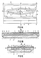
- a lateral transistor according to the invention comprises an emitter region 7 of elongated shape, here in the form of a truncated diamond shape at the center of which is an opening 8 of a thin oxide layer 11, and used for contacting the transmitter.
- the integrated circuit comprises a substrate 1, for example of the p type, in a region of which a buried layer 2 is heavily doped of the opposite type, therefore n+.
- the substrate 1 is covered with an epitaxial layer of opposite type, therefore n, having localized wells, here 4 and 3, respectively forming a well for the lateral transistor and a basic contact well electrically connected to each other. another by the heavily doped buried layer 2.
- the box 3 has a generally rectangular shape and is separated from the box 4 by a deep oxide region 14 which extends to the buried layer 2.
- the box 4 is also of rectangular dimension and is bordered on three sides by a deep oxide region 12 which extends to the buried layer 2, and on the fourth side by the deep oxide region 14.
- the box 3 is bordered on its three non-adjacent sides of the box 4 by the region of deep oxide 12 which thus borders all of the two boxes 3 and 4.
- the box 4 has regions here of type p, forming the emitter 7 and collector regions 6.
- the collector region 6 is bordered externally by the deep oxide layers 12 and 14.
- the base region 5 is constituted by the n-type region of well 4 which remains between regions 6 and 7.
- the opening 8 is, in this case, of square section and its diagonals are arranged along the axes of the rhombus constituting the transmitter 7.
- a contact pad 8 ′ shown in FIGS. 1b and 1c allows contact to be made transmitter.
- the side of the opening 8 has the value L1 and its diagonal 2L5 is the value L1 ⁇ 2.
- L2 be the value of the main half-diagonal of the rhombus and L4 + L5 the value of the other half-diagonal of the rhombus.
- the emitter region 7 has a depth h and a doping level such that the diffusion length of the minority carriers vertically injected into it is greater than or equal to the thickness of this region.
- J1 the lateral injection current density of minority carriers in base 5
- J m the vertical injection current density of minority carriers under the emitter contact area (8)
- J0 la vertical injection current density of minority carriers under the portion of the oxide layer 11 which covers the emitter region 7.
- the value of the gain constantly increases when the ratio between the emitter contact surface and the surface of the emitter region increases. This result is quite surprising for two reasons. On the one hand, it highlights a particular case where the value of the gain does not go through a maximum contrary to the teaching of the aforementioned French patent application 85 19479, and on the other hand the maximum value of the gain ⁇ M is several times higher than that obtained from the above-mentioned request.
- the gain of the transistor is practically only the consequence of the lateral injection induced by the injection under the oxide, this injection under oxide being itself the consequence of the injection under the contact region d 'transmitter. It is precisely the elongated shape of the transmitter in a preferred direction which makes it possible to take full advantage of this phenomenon of injection under the oxide, which was generally perceived as being an undesirable phenomenon.
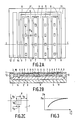
- the transmitter 7 comprises a plurality of bands 7, each band comprising a transmitter contact band forming a plurality of contacts through openings 8.
- the contact pads 8 ′ (not shown) are interconnected by conductive strips themselves interconnected.
- the other substrate elements 1, buried layer 2, wells 3 and 4, etc. have the same reference numbers as in FIGS. 1a to 1c.
- this band structure manifests itself (see section CC of FIG. 2b), by a succession of bands of emitter 7 and collector regions 6 separated by bands of base region 5.
- the collector region strips 6 are interconnected by sections 6 ′.
- the current gain is limited by the emitter resistance induced in the case of FIGS. 1a to 1c, by the length of the emitter, and in the case of FIGS. 2a and 2b, by the spacing between the regions. contact transmitter.
- the emitter resistance tends to lower the maximum admissible current, the current gain starting to drop from a certain level of current. It is therefore necessary to choose in the first case the length of the diamonds and in the second case the spacing between the emitter contacts so as to reconcile a high gain with an acceptable emitter resistance.
- the structure which comprises several bands in parallel makes it possible to multiply the maximum current of the transistor. This structure is therefore particularly advantageous and generally makes it possible to obtain a better optimization than a single-band structure.
- a structure comprising a single emitter band is advantageous for operations at low or very low currents for which only the current gain of the transistor is of importance.
- FIG. 4 represents a variant of the invention, in which the transmitter comprises a strip formed by two truncated diamonds connected together.
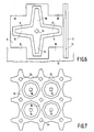
- Figures 5a and 5b show another variant of the invention in which the transmitter comprises two bands each consisting of several truncated diamonds connected together, here three in number per band.
- the transmitter comprises two branches 15 and 16 arranged in two so-called longitudinal directions, at the intersection of which is disposed a transmitter contact 24.
- the two branches 15 and 16 are shown here as two orthogonal diamonds with the same center.
- the perimeter of the emitter is surrounded by the base region 5 itself surrounded by the collector region 6, which comprises an emitter contacting area 19.
- a layer 14 d 'deep oxide separates the box 3 used for making basic contact.
- This structure with two (or more) branches makes it possible to limit the bulk while allowing a reduced emitter resistance, which makes it possible to maintain the high value of the gain at higher currents.
- This arrangement according to several dimensions also has the advantage of being suitable for a checkerboard embodiment, in two or more directions, making it possible to increase the possibilities in current, therefore in power.
- FIG. 7 An embodiment is represented in FIG. 7 according to which elementary structures with two branches according to FIG. 6 are assembled by the end of the branches, constituting in their turn strips arranged in the two longitudinal directions. When there are at least four such strips, at least one collector island can be arranged in the space existing between the strips. In Figure 7, six bands and four islands have been shown. Each island has a collector contact 19.
Landscapes
- Bipolar Transistors (AREA)
Applications Claiming Priority (2)
| Application Number | Priority Date | Filing Date | Title |
|---|---|---|---|
| FR8718388 | 1987-12-30 | ||
| FR8718388A FR2625611B1 (fr) | 1987-12-30 | 1987-12-30 | Circuit integre presentant un transistor lateral |
Publications (2)
| Publication Number | Publication Date |
|---|---|
| EP0322962A1 true EP0322962A1 (de) | 1989-07-05 |
| EP0322962B1 EP0322962B1 (de) | 1994-03-02 |
Family
ID=9358456
Family Applications (1)
| Application Number | Title | Priority Date | Filing Date |
|---|---|---|---|
| EP88202929A Expired - Lifetime EP0322962B1 (de) | 1987-12-30 | 1988-12-19 | Integrierte Schaltung mit einem Lateraltransistor |
Country Status (6)
| Country | Link |
|---|---|
| US (1) | US4951108A (de) |
| EP (1) | EP0322962B1 (de) |
| JP (1) | JPH0793313B2 (de) |
| KR (1) | KR0134778B1 (de) |
| DE (1) | DE3888148T2 (de) |
| FR (1) | FR2625611B1 (de) |
Cited By (3)
| Publication number | Priority date | Publication date | Assignee | Title |
|---|---|---|---|---|
| EP0454248A1 (de) * | 1990-04-27 | 1991-10-30 | Philips Composants | Integrierte Schaltung bestehend aus einem Lateraltransistor mit Mehrfachkollektoren |
| EP0570864A3 (en) * | 1992-05-22 | 1994-07-06 | Siemens Ag | Monolithically integrated pnp transistor structure |
| US5783855A (en) * | 1995-08-18 | 1998-07-21 | Mitsubishi Denki Kabushiki Kaisha | Lateral transistor |
Families Citing this family (11)
| Publication number | Priority date | Publication date | Assignee | Title |
|---|---|---|---|---|
| JPS6243112A (ja) * | 1985-08-20 | 1987-02-25 | 株式会社三英社製作所 | 限流素子ユニツト |
| US5485033A (en) * | 1993-04-07 | 1996-01-16 | U.S. Philips Corporation | Lateral transistor having a particular emitter structure |
| FR2703831A1 (fr) * | 1993-04-07 | 1994-10-14 | Philips Composants | Dispositif semiconducteur comprenant un transistor latéral. |
| US5786622A (en) * | 1997-05-16 | 1998-07-28 | Tritech Microelectronics International Ltd. | Bipolar transistor with a ring emitter |
| TW483171B (en) * | 2000-03-16 | 2002-04-11 | Trw Inc | Ultra high speed heterojunction bipolar transistor having a cantilevered base. |
| US8115280B2 (en) * | 2005-10-31 | 2012-02-14 | Taiwan Semiconductor Manufacturing Company, Ltd. | Four-terminal gate-controlled LVBJTs |
| US8324713B2 (en) * | 2005-10-31 | 2012-12-04 | Taiwan Semiconductor Manufacturing Company, Ltd. | Profile design for lateral-vertical bipolar junction transistor |
| DE102010001788A1 (de) | 2010-02-10 | 2011-08-11 | Forschungsverbund Berlin e.V., 12489 | Skalierbarer Aufbau für laterale Halbleiterbauelemente mit hoher Stromtragfähigkeit |
| CN102315256B (zh) * | 2010-07-08 | 2014-05-14 | 旺宏电子股份有限公司 | 双极接面晶体管装置 |
| US8319315B2 (en) * | 2010-07-30 | 2012-11-27 | Macronix International Co., Ltd. | Bipolar junction transistor devices |
| JP5602890B2 (ja) | 2013-01-29 | 2014-10-08 | ファナック株式会社 | 蓄電装置および抵抗放電装置を有するモータ制御装置 |
Citations (3)
| Publication number | Priority date | Publication date | Assignee | Title |
|---|---|---|---|---|
| US3443173A (en) * | 1966-05-17 | 1969-05-06 | Sprague Electric Co | Narrow emitter lateral transistor |
| GB2077491A (en) * | 1980-05-19 | 1981-12-16 | Hitachi Ltd | Lateral transistors |
| EP0228748A1 (de) * | 1985-12-31 | 1987-07-15 | Philips Composants | Verfahren zum Herstellen eines integrierten lateralen Transistors und eine ihn enthaltende integrierte Schaltung |
Family Cites Families (2)
| Publication number | Priority date | Publication date | Assignee | Title |
|---|---|---|---|---|
| US4231059A (en) * | 1978-11-01 | 1980-10-28 | Westinghouse Electric Corp. | Technique for controlling emitter ballast resistance |
| US4654687A (en) * | 1985-03-28 | 1987-03-31 | Francois Hebert | High frequency bipolar transistor structures |
-
1987
- 1987-12-30 FR FR8718388A patent/FR2625611B1/fr not_active Expired - Fee Related
-
1988
- 1988-12-19 EP EP88202929A patent/EP0322962B1/de not_active Expired - Lifetime
- 1988-12-19 DE DE3888148T patent/DE3888148T2/de not_active Expired - Fee Related
- 1988-12-27 KR KR88017548A patent/KR0134778B1/ko not_active Expired - Fee Related
- 1988-12-27 JP JP63328069A patent/JPH0793313B2/ja not_active Expired - Lifetime
- 1988-12-28 US US07/291,928 patent/US4951108A/en not_active Expired - Fee Related
Patent Citations (3)
| Publication number | Priority date | Publication date | Assignee | Title |
|---|---|---|---|---|
| US3443173A (en) * | 1966-05-17 | 1969-05-06 | Sprague Electric Co | Narrow emitter lateral transistor |
| GB2077491A (en) * | 1980-05-19 | 1981-12-16 | Hitachi Ltd | Lateral transistors |
| EP0228748A1 (de) * | 1985-12-31 | 1987-07-15 | Philips Composants | Verfahren zum Herstellen eines integrierten lateralen Transistors und eine ihn enthaltende integrierte Schaltung |
Cited By (5)
| Publication number | Priority date | Publication date | Assignee | Title |
|---|---|---|---|---|
| EP0454248A1 (de) * | 1990-04-27 | 1991-10-30 | Philips Composants | Integrierte Schaltung bestehend aus einem Lateraltransistor mit Mehrfachkollektoren |
| FR2661556A1 (fr) * | 1990-04-27 | 1991-10-31 | Philips Composants | Circuit integre presentant un transistor lateral multi-collecteurs. |
| EP0570864A3 (en) * | 1992-05-22 | 1994-07-06 | Siemens Ag | Monolithically integrated pnp transistor structure |
| US5783855A (en) * | 1995-08-18 | 1998-07-21 | Mitsubishi Denki Kabushiki Kaisha | Lateral transistor |
| US6060761A (en) * | 1995-08-18 | 2000-05-09 | Mitsubishi Denki Kabushiki Kaisha | Lateral type transistor |
Also Published As
| Publication number | Publication date |
|---|---|
| DE3888148T2 (de) | 1994-09-01 |
| FR2625611B1 (fr) | 1990-05-04 |
| DE3888148D1 (de) | 1994-04-07 |
| US4951108A (en) | 1990-08-21 |
| JPH023241A (ja) | 1990-01-08 |
| FR2625611A1 (fr) | 1989-07-07 |
| KR0134778B1 (en) | 1998-04-20 |
| JPH0793313B2 (ja) | 1995-10-09 |
| EP0322962B1 (de) | 1994-03-02 |
| KR890011101A (ko) | 1989-08-12 |
Similar Documents
| Publication | Publication Date | Title |
|---|---|---|
| EP0322962B1 (de) | Integrierte Schaltung mit einem Lateraltransistor | |
| US3422527A (en) | Method of manufacture of high voltage solar cell | |
| FR2481519A1 (fr) | Dispositif photovoltaique et procede de fabrication | |
| FR2494499A1 (fr) | Structure plane pour dispositifs semi-conducteurs a haute tension | |
| EP0140772A2 (de) | PIN-Dioden als Leistungsbegrenzer für Millimeterwellen und Verfahren zum Herstellen der Dioden | |
| EP0038238A1 (de) | Verfahren zur Herstellung einer Halbleiteranordnung mit von der Oberfläche aus zugänglichem, tief eingebettetem Gitter | |
| US4029962A (en) | Arrays for infrared image detection | |
| FR2853454A1 (fr) | Transistor mos haute densite | |
| JPH11510318A (ja) | ホトダイオード及びその製造方法 | |
| US4004949A (en) | Method of making silicon solar cells | |
| FR2739976A1 (fr) | Structure de terminaison, dispositif a semi-conducteur, et leurs procedes de fabrication | |
| FR2531572A1 (fr) | Dispositif mos a structure plane multicellulaire | |
| US5633526A (en) | Photodiode array and method for manufacturing the same | |
| FR2640081A1 (fr) | Transistor a effet de champ vertical | |
| EP0115650B1 (de) | Leistungs-MOS-Feldeffekttransistor mit einer planaren multi-zellularen Struktur | |
| EP1142023B1 (de) | Randstruktur für monolithische Leistungsanordnung | |
| EP0002087B1 (de) | Monolithische Halbleiteranordnung mit zwei komplementären Transistoren und Verfahren zur Herstellung derselben | |
| EP0185426B1 (de) | Integrierte Schaltung, die eine Schutzanordnung gegen elektrostatische Entladungen enthält | |
| EP0228748B1 (de) | Verfahren zum Herstellen eines integrierten lateralen Transistors und eine ihn enthaltende integrierte Schaltung | |
| EP0546889B1 (de) | Stromzuführungssystem für eine integrierte Halbleiterlaser-Schaltung | |
| FR2495380A1 (fr) | Dispositif de memoire a semiconducteur | |
| EP0373066A1 (de) | Symmetrische Halbleiterleistungseinrichtung und Verfahren zu deren Herstellung | |
| EP0077706A1 (de) | Feldeffekttransistor mit vertikalem Kanal | |
| EP0454248B1 (de) | Integrierte Schaltung bestehend aus einem Lateraltransistor mit Mehrfachkollektoren | |
| JPH07162022A (ja) | 半導体受光素子、その製造方法および半導体の加工方法 |
Legal Events
| Date | Code | Title | Description |
|---|---|---|---|
| PUAI | Public reference made under article 153(3) epc to a published international application that has entered the european phase |
Free format text: ORIGINAL CODE: 0009012 |
|
| AK | Designated contracting states |
Kind code of ref document: A1 Designated state(s): DE FR GB IT NL |
|
| 17P | Request for examination filed |
Effective date: 19891220 |
|
| RAP1 | Party data changed (applicant data changed or rights of an application transferred) |
Owner name: N.V. PHILIPS' GLOEILAMPENFABRIEKEN Owner name: PHILIPS COMPOSANTS |
|
| 17Q | First examination report despatched |
Effective date: 19920825 |
|
| RAP1 | Party data changed (applicant data changed or rights of an application transferred) |
Owner name: N.V. PHILIPS' GLOEILAMPENFABRIEKEN Owner name: PHILIPS COMPOSANTS |
|
| GRAA | (expected) grant |
Free format text: ORIGINAL CODE: 0009210 |
|
| AK | Designated contracting states |
Kind code of ref document: B1 Designated state(s): DE FR GB IT NL |
|
| PG25 | Lapsed in a contracting state [announced via postgrant information from national office to epo] |
Ref country code: NL Effective date: 19940302 |
|
| REF | Corresponds to: |
Ref document number: 3888148 Country of ref document: DE Date of ref document: 19940407 |
|
| ITF | It: translation for a ep patent filed | ||
| GBT | Gb: translation of ep patent filed (gb section 77(6)(a)/1977) |
Effective date: 19940607 |
|
| NLV1 | Nl: lapsed or annulled due to failure to fulfill the requirements of art. 29p and 29m of the patents act | ||
| PLBE | No opposition filed within time limit |
Free format text: ORIGINAL CODE: 0009261 |
|
| STAA | Information on the status of an ep patent application or granted ep patent |
Free format text: STATUS: NO OPPOSITION FILED WITHIN TIME LIMIT |
|
| 26N | No opposition filed | ||
| ITPR | It: changes in ownership of a european patent |
Owner name: CAMBIO RAGIONE SOCIALE;PHILIPS ELECTRONICS N.V. |
|
| REG | Reference to a national code |
Ref country code: FR Ref legal event code: CD |
|
| PGFP | Annual fee paid to national office [announced via postgrant information from national office to epo] |
Ref country code: GB Payment date: 19981218 Year of fee payment: 11 |
|
| PGFP | Annual fee paid to national office [announced via postgrant information from national office to epo] |
Ref country code: FR Payment date: 19981222 Year of fee payment: 11 |
|
| PGFP | Annual fee paid to national office [announced via postgrant information from national office to epo] |
Ref country code: DE Payment date: 19990217 Year of fee payment: 11 |
|
| PG25 | Lapsed in a contracting state [announced via postgrant information from national office to epo] |
Ref country code: GB Free format text: LAPSE BECAUSE OF NON-PAYMENT OF DUE FEES Effective date: 19991219 |
|
| GBPC | Gb: european patent ceased through non-payment of renewal fee |
Effective date: 19991219 |
|
| PG25 | Lapsed in a contracting state [announced via postgrant information from national office to epo] |
Ref country code: FR Free format text: LAPSE BECAUSE OF NON-PAYMENT OF DUE FEES Effective date: 20000831 |
|
| PG25 | Lapsed in a contracting state [announced via postgrant information from national office to epo] |
Ref country code: DE Free format text: LAPSE BECAUSE OF NON-PAYMENT OF DUE FEES Effective date: 20001003 |
|
| REG | Reference to a national code |
Ref country code: FR Ref legal event code: ST |
|
| PG25 | Lapsed in a contracting state [announced via postgrant information from national office to epo] |
Ref country code: IT Free format text: LAPSE BECAUSE OF NON-PAYMENT OF DUE FEES;WARNING: LAPSES OF ITALIAN PATENTS WITH EFFECTIVE DATE BEFORE 2007 MAY HAVE OCCURRED AT ANY TIME BEFORE 2007. THE CORRECT EFFECTIVE DATE MAY BE DIFFERENT FROM THE ONE RECORDED. Effective date: 20051219 |