EP0323183A2 - Integrierte Schaltung mit photoempfindlichen Zellen - Google Patents
Integrierte Schaltung mit photoempfindlichen Zellen Download PDFInfo
- Publication number
- EP0323183A2 EP0323183A2 EP88312284A EP88312284A EP0323183A2 EP 0323183 A2 EP0323183 A2 EP 0323183A2 EP 88312284 A EP88312284 A EP 88312284A EP 88312284 A EP88312284 A EP 88312284A EP 0323183 A2 EP0323183 A2 EP 0323183A2
- Authority
- EP
- European Patent Office
- Prior art keywords
- printing
- photo
- cells
- sensor cells
- data
- Prior art date
- Legal status (The legal status is an assumption and is not a legal conclusion. Google has not performed a legal analysis and makes no representation as to the accuracy of the status listed.)
- Withdrawn
Links
Images


Classifications
-
- H—ELECTRICITY
- H04—ELECTRIC COMMUNICATION TECHNIQUE
- H04N—PICTORIAL COMMUNICATION, e.g. TELEVISION
- H04N1/00—Scanning, transmission or reproduction of documents or the like, e.g. facsimile transmission; Details thereof
- H04N1/024—Details of scanning heads ; Means for illuminating the original
- H04N1/02418—Details of scanning heads ; Means for illuminating the original for picture information pick up and reproduction
- H04N1/02463—Details of scanning heads ; Means for illuminating the original for picture information pick up and reproduction using heads mounted on the same support or substrate
-
- H—ELECTRICITY
- H04—ELECTRIC COMMUNICATION TECHNIQUE
- H04N—PICTORIAL COMMUNICATION, e.g. TELEVISION
- H04N1/00—Scanning, transmission or reproduction of documents or the like, e.g. facsimile transmission; Details thereof
- H04N1/024—Details of scanning heads ; Means for illuminating the original
-
- H—ELECTRICITY
- H04—ELECTRIC COMMUNICATION TECHNIQUE
- H04N—PICTORIAL COMMUNICATION, e.g. TELEVISION
- H04N1/00—Scanning, transmission or reproduction of documents or the like, e.g. facsimile transmission; Details thereof
- H04N1/04—Scanning arrangements, i.e. arrangements for the displacement of active reading or reproducing elements relative to the original or reproducing medium, or vice versa
- H04N1/207—Simultaneous scanning of the original picture and the reproduced picture with a common scanning device
-
- H—ELECTRICITY
- H10—SEMICONDUCTOR DEVICES; ELECTRIC SOLID-STATE DEVICES NOT OTHERWISE PROVIDED FOR
- H10F—INORGANIC SEMICONDUCTOR DEVICES SENSITIVE TO INFRARED RADIATION, LIGHT, ELECTROMAGNETIC RADIATION OF SHORTER WAVELENGTH OR CORPUSCULAR RADIATION
- H10F39/00—Integrated devices, or assemblies of multiple devices, comprising at least one element covered by group H10F30/00, e.g. radiation detectors comprising photodiode arrays
- H10F39/10—Integrated devices
- H10F39/12—Image sensors
- H10F39/18—Complementary metal-oxide-semiconductor [CMOS] image sensors; Photodiode array image sensors
Definitions
- the present invention relates to a semi-conductor device suitable for use in apparatus providing input/output functions for characters and graphics, such as facsimile apparatus and a word processor.
- Information processing apparatus providing the functions of reading characters and graphic information as image data and then printing out such data has been put into practical use both in the form of facsimile apparatus (hereinafter referred to as a fax machine) and in the form of a word processor.
- Such apparatus usually comprises photo-sensors for converting image data into electrical signals, logic circuits for processing and controlling the output signals of the photo-sensors, printing cells for printing given printing data onto a predetermined recording medium and drive circuits for driving the printing cells in accordance with the printing data, but each of these hardware elements is formed separately and they are subsequently built into a case.
- a device comprises a plurality of photo-sensor cells for reading image data, drive means for driving printing cells in printing means, and control means for controlling the drive means in response to received printing data and for processing output signals from the photo-sensor cells, characterised in that the device is a semi-conductor device, in which the photo-sensor cells, the drive means and the control means are formed on a single substrate as integrated circuits.
- the image data may be converted into electrical data by the photo-sensor cells, and the converted data may be processed and supplied to external circuits.
- the semi-conductor device is adapted to be responsive to the printing data for controlling printing by driving a printing device such as a thermal printing head through the drive means.
- a semi-conductor device comprises, as an integrated circuit on a single substrate, a plurality of photo-sensor cells for reading image data such as characters and figures, a plurality of drive cells for driving respectively a plurality of printing cells to print determined images, and control circuits for controlling the photo-sensor cells and the drive cells.
- Figure 1 shows a semi-conductor device according to the present invention applied to an image sensor 1 of a fax machine or similar apparatus.
- the image sensor 1 comprises an n-bit line image sensor 2 forming a part of an integrated circuit semi-conductor device having a single semi-conductor substrate 3.
- Photo-sensor cells (21, 22...2 n ) forming the line image sensor 2 are respectively arranged within unit blocks 31, 32...3 n arranged to form lines on the semi-conductor substrate 3.
- the unit blocks 31, 32...3 n have almost the same structure and therefore only the unit blocks 31, 32 are shown in Figure 2 in detail.
- each unit block, 31 is as follows.
- a Q output terminal of a D type flip-flop 111 (hereinafter abbreviated as FF) is connected to a D input terminal of a latch circuit 131, while an external latch/terminal 8 is connected to a clock input terminal (CLK) of the latch circuit 131.
- a Q output terminal of the latch circuit 131 is connected to one input terminal of an enable gate 141 and another input terminal of the enable gate 141 is connected to an external enable terminal 9.
- An output terminal of the enable gate 141 is connected to an input terminal of a drive cell 161, while an output terminal of the drive cell 161 is connected to an external drive output terminal 61.
- the Q output terminal of the FF 111 is also connected to one input terminal of an AND gate 121, another input terminal of the AND gate 121 being connected to a clock input terminal (CLK) of the FF 111.
- An output terminal of the AND gate 121 is connected to a control terminal of a transfer gate 151 and an output terminal of the photo-sensor cell 21 is connected to an input terminal of the transfer gate 151.
- An output terminal of the transfer gate 151 is connected to an external terminal 7 through a common output line 171.
- a plurality of such unit blocks are connected to form the circuit of the present invention.
- the FF 111 is connected so that it corresponds to a single stage of a shift register.
- the D input of the FF 111 of the unit block in the first stage is connected to a data input terminal 4.
- the common output line 171, 172...17 n of each unit block is connected so as to be at the same potential as the external terminal 7.
- the clock input terminal of each FF 111, 112...11 n is connected to an external clock input terminal 5, while the clock input terminal of each latch circuit 131, 132...13 n is connected to the latch strobe terminal 8 in common and the external enable terminal 9 is connected to one input terminal of each enable gate 141, 142...14 n in common.
- the drive cells 161, 162...16 n thus form a drive circuit, which although not illustrated drives printing cells, for example in a thermal printing head, and the photo-sensor cells, 21, 22...2 n thus form the line image sensor.
- the other circuits 111, 112...11 n ; 121, 122...12 n ; 131, 132...13 n ; 141, 142...14 n ; 151, 152...15 n respectively form the control circuits.
- the printing data is synchronised with the clock signal of the shift register formed by the FFs 111, 112...11 n connected to the data input terminal 4 and is transferred to each unit block in turn.
- the printing data transferred to each block appears at the Q output of the respective FF 11 i , and application of a control signal "ON" to the latch strobe terminal 8 holds such data in order to supply the printing data from each block to the respective latch circuits.
- a control signal "OFF" is applied to the latch strobe terminal 8, establishing the condition to input the printing data to the FFs.
- a control signal "ON" is input to the enable terminal 9 in order to switch the enable gate 14 i into an ON condition and operate the drive cell 16 i to drive the heat generating cell through the drive output terminal 6 i connected to the output terminal of the drive cell 16 i .
- the driving of the heat generating cell can be terminated when printing is complete. New data can then be printed by repeating these operations.
- N-bit serial data (1000...0) is applied to the terminal 4, which is the data input terminal of the shift register, and is then sequentially read to each stage of the shift register in synchronisation with the clock signal by applying clock pulses continuously to the clock terminal 5.
- the transfer gates 151, 152...15 n are sequentially turned ON and the image data obtained by the photo-sensor cells 21, 22...2 n is sequentially output from the output terminal 7.
- the "OFF" signal is applied continuously to both the latch strobe and the enable terminals 8, 9 so that the drive cells for printing are not turned on.
- the drive circuits for driving the printing cells and the control circuits for controlling the printing cells are structured on the same substrate, in addition to the image sensor 2, thereby realising a reduction in size.
- these components since these components all comprise semi-conductor elements, they can be formed as an integrated circuit on a single crystal substrate, thus resulting in a cost reduction through a simplified manufacturing process and providing a low cost device having a small size.
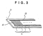
- Figure 3 shows an example of the device in which N image sensors 1, of which one is illustrated in Figure 1, are provided in series on a ceramic substrate 21 carrying a heat generating cell array 20 for printing, and in which the drive output terminal 61, 62...6 n of each image sensor 1 are connected to each heat generating cell of the heat generating array 20 by a group of wires 22 on a one to one basis.
- circuit portions manufactured in the same semi-conductor integrated circuit process are formed on the same substrate as the image sensor. Therefore, not only can the size of the device be reduced, but also only a single manufacturing process is required. Accordingly, the manufacturing cost can be reduced remarkably in comparison with the known manufacturing process, in which the circuit components are produced separately.
Landscapes
- Engineering & Computer Science (AREA)
- Multimedia (AREA)
- Signal Processing (AREA)
- Facsimile Heads (AREA)
- Light Receiving Elements (AREA)
- Solid State Image Pick-Up Elements (AREA)
Applications Claiming Priority (2)
| Application Number | Priority Date | Filing Date | Title |
|---|---|---|---|
| JP332504/87 | 1987-12-29 | ||
| JP62332504A JP2717249B2 (ja) | 1987-12-29 | 1987-12-29 | 画像読取印字装置 |
Publications (2)
| Publication Number | Publication Date |
|---|---|
| EP0323183A2 true EP0323183A2 (de) | 1989-07-05 |
| EP0323183A3 EP0323183A3 (de) | 1990-08-22 |
Family
ID=18255674
Family Applications (1)
| Application Number | Title | Priority Date | Filing Date |
|---|---|---|---|
| EP88312284A Withdrawn EP0323183A3 (de) | 1987-12-29 | 1988-12-23 | Integrierte Schaltung mit photoempfindlichen Zellen |
Country Status (3)
| Country | Link |
|---|---|
| US (1) | US5060084A (de) |
| EP (1) | EP0323183A3 (de) |
| JP (1) | JP2717249B2 (de) |
Cited By (3)
| Publication number | Priority date | Publication date | Assignee | Title |
|---|---|---|---|---|
| EP0365312A3 (de) * | 1988-10-20 | 1991-01-16 | Canon Kabushiki Kaisha | Halbleiteranordnung und eine Signalbehandlungsvorrichtung mit dieser Anordnung |
| EP0465216A3 (en) * | 1990-07-02 | 1992-08-05 | Xerox Corporation | Compact read/write scanner |
| EP0917341A4 (de) * | 1996-07-30 | 1999-07-14 | Rohm Co Ltd | Bildlese/aufzeichnungskopf und dafür benutzter integrierter schaltkreis |
Families Citing this family (3)
| Publication number | Priority date | Publication date | Assignee | Title |
|---|---|---|---|---|
| US5491566A (en) * | 1992-11-27 | 1996-02-13 | Goldstar Co., Ltd. | Integrated input-output device having a reading and a printing section on a single substrate |
| JPH10285331A (ja) * | 1997-04-10 | 1998-10-23 | Canon Inc | イメージセンサおよびこのイメージセンサを用いた情報処理装置 |
| KR102739824B1 (ko) * | 2019-11-21 | 2024-12-09 | 에스케이하이닉스 주식회사 | 온도 감지 회로를 포함하는 반도체 장치 |
Family Cites Families (8)
| Publication number | Priority date | Publication date | Assignee | Title |
|---|---|---|---|---|
| JPS5639675A (en) * | 1979-09-06 | 1981-04-15 | Ricoh Co Ltd | Facsimile equipment and its head |
| DE3269826D1 (en) * | 1981-08-17 | 1986-04-17 | Xerox Corp | Imaging device |
| DE3339256A1 (de) * | 1982-11-01 | 1984-05-10 | Canon K.K., Tokio/Tokyo | Bildeingabevorrichtung |
| JPS5983462A (ja) * | 1982-11-04 | 1984-05-14 | Fuji Xerox Co Ltd | 読取印字複写装置 |
| US4706128A (en) * | 1983-12-14 | 1987-11-10 | Canon Kabushiki Kaisha | Image reading and converting apparatus |
| JPS61104868A (ja) * | 1984-10-29 | 1986-05-23 | Hitachi Ltd | 感熱記録ヘツド |
| JPS61152160A (ja) * | 1984-12-26 | 1986-07-10 | Hitachi Ltd | フアクシミリ装置 |
| EP0246481B1 (de) * | 1986-05-13 | 1990-12-27 | Heimann GmbH | Kontaktbildsensorzeile |
-
1987
- 1987-12-29 JP JP62332504A patent/JP2717249B2/ja not_active Expired - Lifetime
-
1988
- 1988-12-23 EP EP88312284A patent/EP0323183A3/de not_active Withdrawn
- 1988-12-23 US US07/289,185 patent/US5060084A/en not_active Expired - Lifetime
Cited By (4)
| Publication number | Priority date | Publication date | Assignee | Title |
|---|---|---|---|---|
| EP0365312A3 (de) * | 1988-10-20 | 1991-01-16 | Canon Kabushiki Kaisha | Halbleiteranordnung und eine Signalbehandlungsvorrichtung mit dieser Anordnung |
| EP0465216A3 (en) * | 1990-07-02 | 1992-08-05 | Xerox Corporation | Compact read/write scanner |
| EP0917341A4 (de) * | 1996-07-30 | 1999-07-14 | Rohm Co Ltd | Bildlese/aufzeichnungskopf und dafür benutzter integrierter schaltkreis |
| US6222581B1 (en) | 1996-07-30 | 2001-04-24 | Rohm Co., Ltd. | Picture reading/writing head and integrated circuit used for the same |
Also Published As
| Publication number | Publication date |
|---|---|
| JP2717249B2 (ja) | 1998-02-18 |
| EP0323183A3 (de) | 1990-08-22 |
| US5060084A (en) | 1991-10-22 |
| JPH01175254A (ja) | 1989-07-11 |
Similar Documents
| Publication | Publication Date | Title |
|---|---|---|
| US5060071A (en) | Full-size optical sensor device having improved driving means | |
| KR950009816B1 (ko) | 광전변환장치 | |
| JP2862592B2 (ja) | ディスプレイ装置 | |
| US4961169A (en) | Method of and apparatus for generating variable time delay | |
| JPH05167777A (ja) | カラーセンサーアレイ多重化配列 | |
| EP0323183A2 (de) | Integrierte Schaltung mit photoempfindlichen Zellen | |
| US5027226A (en) | Contact type image sensor | |
| JP2646974B2 (ja) | 走査回路およびその駆動方法 | |
| JP3068394B2 (ja) | センサシステム | |
| US5105450A (en) | Charge transfer device having alternating large and small transfer electrodes | |
| KR0178521B1 (ko) | 리니어 이미지 센서 | |
| US5109440A (en) | Image sensing apparatus | |
| US7015449B2 (en) | Linear image sensor | |
| KR19980701945A (ko) | 멀티플렉서 회로 | |
| JP3703712B2 (ja) | イメージセンサ | |
| US4573079A (en) | Sensor array driving circuit | |
| US7721169B2 (en) | Scan circuit and image sensor having scan circuit | |
| US4862275A (en) | Readout of charge packets from area imager CCD using an inverter-chain shift register | |
| US4103345A (en) | Semiconductor memory with data detection circuit | |
| JPS6320951A (ja) | イメ−ジ・センサ | |
| JPH0584971B2 (de) | ||
| JPH0271561A (ja) | 密着型等倍センサ | |
| US6404938B1 (en) | Dummy clock control method and apparatus for a sequential I/O device | |
| JPS6126361A (ja) | イメ−ジセンサ | |
| JPH088727A (ja) | 一致検出回路 |
Legal Events
| Date | Code | Title | Description |
|---|---|---|---|
| PUAI | Public reference made under article 153(3) epc to a published international application that has entered the european phase |
Free format text: ORIGINAL CODE: 0009012 |
|
| AK | Designated contracting states |
Kind code of ref document: A2 Designated state(s): DE FR GB |
|
| PUAL | Search report despatched |
Free format text: ORIGINAL CODE: 0009013 |
|
| RHK1 | Main classification (correction) |
Ipc: H01L 49/02 |
|
| AK | Designated contracting states |
Kind code of ref document: A3 Designated state(s): DE FR GB |
|
| 17P | Request for examination filed |
Effective date: 19901228 |
|
| 17Q | First examination report despatched |
Effective date: 19930630 |
|
| STAA | Information on the status of an ep patent application or granted ep patent |
Free format text: STATUS: THE APPLICATION IS DEEMED TO BE WITHDRAWN |
|
| 18D | Application deemed to be withdrawn |
Effective date: 19950701 |