EP0323675A1 - Einseitenbandsignal-Generatoranordnung - Google Patents
Einseitenbandsignal-Generatoranordnung Download PDFInfo
- Publication number
- EP0323675A1 EP0323675A1 EP19880203015 EP88203015A EP0323675A1 EP 0323675 A1 EP0323675 A1 EP 0323675A1 EP 19880203015 EP19880203015 EP 19880203015 EP 88203015 A EP88203015 A EP 88203015A EP 0323675 A1 EP0323675 A1 EP 0323675A1
- Authority
- EP
- European Patent Office
- Prior art keywords
- frequency
- interpolating
- interpolating means
- samples
- ssb
- Prior art date
- Legal status (The legal status is an assumption and is not a legal conclusion. Google has not performed a legal analysis and makes no representation as to the accuracy of the status listed.)
- Granted
Links
- 238000005070 sampling Methods 0.000 claims abstract description 39
- 238000000034 method Methods 0.000 abstract description 14
- 239000000523 sample Substances 0.000 description 8
- 238000010586 diagram Methods 0.000 description 7
- 230000005540 biological transmission Effects 0.000 description 3
- 230000002238 attenuated effect Effects 0.000 description 2
- 230000010354 integration Effects 0.000 description 2
- 230000004048 modification Effects 0.000 description 2
- 238000012986 modification Methods 0.000 description 2
- 238000009825 accumulation Methods 0.000 description 1
- 238000006243 chemical reaction Methods 0.000 description 1
- 230000003111 delayed effect Effects 0.000 description 1
- 238000001514 detection method Methods 0.000 description 1
- 230000000694 effects Effects 0.000 description 1
- 238000001914 filtration Methods 0.000 description 1
- 230000007274 generation of a signal involved in cell-cell signaling Effects 0.000 description 1
Images


Classifications
-
- H—ELECTRICITY
- H03—ELECTRONIC CIRCUITRY
- H03C—MODULATION
- H03C1/00—Amplitude modulation
- H03C1/52—Modulators in which carrier or one sideband is wholly or partially suppressed
- H03C1/60—Modulators in which carrier or one sideband is wholly or partially suppressed with one sideband wholly or partially suppressed
-
- H—ELECTRICITY
- H03—ELECTRONIC CIRCUITRY
- H03C—MODULATION
- H03C2200/00—Indexing scheme relating to details of modulators or modulation methods covered by H03C
- H03C2200/0037—Functional aspects of modulators
- H03C2200/0058—Quadrature arrangements
-
- H—ELECTRICITY
- H03—ELECTRONIC CIRCUITRY
- H03C—MODULATION
- H03C2200/00—Indexing scheme relating to details of modulators or modulation methods covered by H03C
- H03C2200/0037—Functional aspects of modulators
- H03C2200/007—Functional aspects of modulators with one sideband wholly or partially suppressed
Definitions
- the present invention relates to an arrangement for generating an SSB signal and has applications in both the analogue and conventional digital implementations single sideband modulators constructed in accordance with what is termed Weaver's method. Such modulators are used in SSB generation in speech and data transmission for mobile radios.
- FIG. 1 of the accompanying drawings illustrates a modulator made in accordance with Weaver's method.
- An analogue input signal at an input 10 is band limited in a bandpass filter 12 and then is applied to balanced mixers 14, 16 where it is mixed with quadrature related carrier signals cos ( ⁇ o t) and sin ( ⁇ o t), where ⁇ o t is a carrier frequency corresponding to the centre of the passband of the signal from the filter 12.
- quadrature related signals I and Q are produced which have single sideband components at base band and unwanted components at high frequencies.
- the wanted components of the I and Q signals are selected by low pass filters 18, 20 and then frequency up-converted to their carrier frequency ( ⁇ c t) in balanced mixers 22, 24.
- the signals from these mixers are combined in a summing circuit 25 to provide an output on a terminal 26.
- a drawback to Weaver's method is that it is difficult to implement the frequency up-converting or RF section as an integrated circuit.
- Reasons for this difficulty include the fact that matching of the mixers 22, 24 ( Figure 1) is complicated and it may be necessary to run the mixers at a high power level to achieve the desired performance. Also it is necessary to make a pair of quadarature local oscillators capable of generating a wide range of frequencies. Any mismatch in the mixers or any imperfection in the quadrature RF signal generation may cause the unwanted signal levels to increase.
- the I and Q signals from the mixers are low pass filtered in digital filters 18, 20 which are clocked at the frequency f s1 which satisfies the Nyquist sampling rate.
- the output signals which have been sampled at f s1 are applied to respective interpolators 30, 32 operating at a sampling frequency Nf s .
- the outputs of the interpolators 30, 32 are frequency up-converted in digital multipliers 34, 36 to which are supplied quadrature carrier signals cos [2 ⁇ f c .(n/Nf s )] and sin [2 ⁇ f c .(n/Nf s )], respectively.
- the outputs from the digital multipliers 34, 36 are combined in the summing circuit 25 and the R.F. output appears on the terminal 26.
- An object of the present invention is to provide an integratable SSB generator which is economical on its use of power.
- an SSB generator comprising means for providing quadrature related digitised first and second input signals at baseband frequencies, interpolating means for frequency up-converting said first and second signals, and multiplexing means coupled to the interpolating means for multiplexing the frequency up-converted first and second input signals to provide a digitised SSB signal having a desired carrier frequency.
- the interpolating means may comprise first and second interpolating means, the first interpolating means serving to sample respectively the first and second signals at a frequency (f s ) greater than the digitising frequency and the second interpolating means serving to sample the signals from the first interpolating means at a multiple of the first mentioned sampling frequency.
- the multiplexing means may be arranged to multiplex the samples at the sampling frequency of the second interpolating means.
- the interpolating means operates as a digital filter and serves to increase the repetition rate of the signal from a digital low pass filter to make it suitable for linear interpolation in the second interpolating means.
- the second interpolating means operates as a linear interpolator which lifts the frequency up to RF.
- the sampling frequency used in the second interpolation operation is 4N times the sampling frequency (f s ) used in the first interpolation operation, that is 4Nf s , and the multiplexing operation is carried out at a clock frequency of 4Nf s to provide the SSB signal at Nf s .
- the multiplexed output may be interpolated for a third time in order to shift the sampling frequency 4Nf s to a higher frequency outside the bandwidth of a low pass filter connected to a digital to analogue converter coupled to the multiplexing means.
- the second interpolation means may be adapted to calculate the values of all the samples of the frequency up-converted first and second digitised signals. Alternatively power can be saved by only calculating the values of those samples which after multiplexing will contribute to the final signal. In order to do this only the odd-numbered samples in one of the first and second interpolated signals are calculated and only the even-numbered samples in the other of the first and second interpolated signals are calculated.
- the SSB modulator shown is essentially the same as that shown in Figure 2 as far as the interpolators 30, 32 which are operating at a sampling frequency, f s , which is of the order of 30 times higher than the frequency at the top end of the bandwidth of the low pass filters 18, 20.
- the outputs from the interpolators 30, 32 are applied to second interpolators 38, 40 operating at a higher sampling frequency, Nf s , than f s .
- the outputs from the second interpolators 38, 40 are multiplexed in multiplexer 42 to provide an output comprising the SSB signal centred on Nf s /4 plus the sampling frequency component in the output from the multiplexer, the output is applied to a third interpolator 44 which has a sampling frequency which is an integer multiple of Nfs.
- a digital to analogue converter 46 is connected to the third interpolator 44 and provides an output on the terminal 26.
- Figure 4 shows the impulse response of an interpolating filter which may comprise the second interpolator 38 or 40.
- the ordinate represents amplitude and the abscissa time.
- the response shape is sampled at N times the sampling frequency f s , that is at Nf s .
- the frequency response of the interpolating filter has zero crossings at each integer multiple of f s , but the signal at Nf s will not be attenuated.
- the filter when the signal samples, sampled at f s , are applied to the interpolating filter, the filter as a consequence will eliminate all the signals between f s and Nf s .
- the output produced comprises an interpolated version of the input signal having a new sampling frequency of Nf s .
- N is determined by the highest required integer number used to increase the sampling frequency f s .
- the filter response length is -T s to T s which equals 2/f s .
- T s 1/f s . Therefore in realising the interpolating filter as a transversal filter only two multipliers at a time are required together with an addition circuit to sum the multiplied signal samples.
- sampling frequency f s is to be increased by a factor of N, then one obtains the difference between adjacent samples, x1 and x2, at the sampling frequency f s and divide the result by the interpolation factor, N. The resulting quotient is then taken as an increment and added to the sample x2 at every instant n to produce the interpolated samples of the input signal at the new sampling frequency Nf s .
- the signal sampled at f s is applied to a shift-register or tapped delay line 48.
- Samples x1 and x2 separated by 1/f s seconds are tapped off and applied to a subtractor 50 which produces the difference or increment (x1-x2) which is applied to a divider 52 in which the increment is divided by N.
- the quotient from the divider is added to the sample x2 in an accumulator 54 to produce the interpolated samples of the input signal at the new sampling frequency Nf s .
- FIG 9 is a block schematic diagram of an SSB modulator made in accordance with the present invention.
- the front end portion corresponds to that described with reference to and as shown in Figure 3 and in the interests of brevity will not be described again.
- the second interpolators 38, 40 are based on the circuit as shown in Figure 8 with some modifications.
- the circuit stages which correspond to those used in the second interpolator 38 have been referenced using primed reference numerals, that is 48′, 50′, 52′ and 54′.
- the differences are divided by 4N in the dividers 52 and 52′ and the accumulators 54, 54′ are clocked at 4Nf s . The effect of doing this is that the increment is obtained by dividing the difference by 4N.
- the increment is then accumulated on the delayed signal sample x2 at regular clocking points.
- the accumulation starts every time a new sample is loaded into the shift register or tapped delay line 48, 48′ and continues for 4N clock periods until a new sample is loaded into the shift register so that the process is repeated for a new value of x2.
- the clock signal 4Nf s is derived from a master clock 56 operating at a higher frequency than 4Nf s and divided down in a divider 58. This divided down signal at 4Nf s is divided by 4N in another divider 60 to provide clock signals at f s , where f s has a value of the order of 100KHz, to the interpolators 30, 32.
- the clock signal f s1 for the A to D converter 28 and the digital low pass filters 18, 20 is derived by dividing f s by m, where m is of the order of 8, in a divider 62.
- the multiplexer 42 provides an SSB signal at a nominal carrier frequency Nf s sampled at 4Nf s .
- the multiplexer 42 comprises the electronic equivalent of four pole switch 64 operating at 4Nf s . Proceeding from top to bottom in Figure 9, the first and second poles are respectively connected to addition stages 66, 66′ of the second interpolators 38, 40 which stages provide digital values of the samples. The third and fourth poles provide inverted forms of the signals on the first and second poles, respectively.
- the output from the multiplexer 42 comprises a digitised form of the SSB signal at the nominal carrier frequency Nf s and the unwanted sampling frequency at 4Nf s .
- the multiplexer output is applied to the third interpolator 44 in which it is sampled at the clock frequency of the master clock 56, which frequency is above the bandwidth of a low pass filter 68 connected to the output of the D to A converter 46.
- the sampling frequency 4Nf s is eliminated by interpolation so that it is outside the bandwidth of the low pass filter 68.
- the required quadrature oscillator samples will be 1, 0, -1, 0, 1, 0 and 0, 1, 0, -1, 0,1 in the I and Q channels, respectively.
- these I and Q signal samples appearing at the outputs of the base band filters 18, 20 are interpolated to a sampling frequency 4Nf s in the interpolators 30, 38 and 32, 40. These samples are multiplied with the RF oscillator samples (see above) so that the alternate products of the multiplication in the I and Q channels become equal to zero.
- the multiplexer 42 selects samples alternately from the I and Q channels, which samples after D to A conversion and filtering form the SSB signal on the output 26.
- the SSB signal sampling frequency 4Nf s is selected to be 4 times higher than f c .
- the sampling frequency f s for the interpolators 30, 32 is chosen by dividing 4Nf s by 4N in the stage 60.
- the frequency f s1 is produced by dividing f s by m in the stage 62.
- the master clock frequency is generated using a phase locked loop.
- the local oscillator frequency f1 is kept constant.
- the values of m and f s1 are maintained at 8 and 12.5kHz, respectively.
- the interpolation factor and the sampling frequency of the third interpolator 44 are set to 3 and 12 MHz, respectively.
- the divider 58 divides the 12 MHz by 3 to obtain the desired 4Nf s .
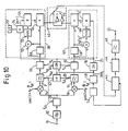
- the second I and Q interpolators 38, 40 are operated at 2f s and the signals are multiplexed at 4Nf s .
- the master clock 56 is connected to the divider 58 which produces an output signal at 2NF s .
- the multiplexer 42 is still clocked at 4Nf s .
- the signal at 2Nf s is supplied firstly to the divider 60 where it is divided down by 2N to provide the clock signal f s to the interpolators 30, 32 and secondly to increment a counter 70 two steps at a time.
- the counter 70 is reset at the instants when data is loaded into the shift registers 48, 48′.
- the output of the counter 70 is applied to a multiplier 54′ and to an adder 74 in which it is added to +1 provided by a stage 72.
- the sum 2n+1 is supplied to the multiplier 54.
- the multiplier 54 the number obtained from the divider is multiplied by 2n+1 to produce the increments for the I channel.
- the output of the divider 52′ is multiplied by 2n to produce the increments for the Q channel.
- the SSB modulators shown in Figures 9 and 10 are capable of being fabricated as integrated circuits. If desired a signal processor may be used to realise the base band mixers 14, 16 and the interpolators 30,32, 38 and 40.
Landscapes
- Amplitude Modulation (AREA)
- Digital Transmission Methods That Use Modulated Carrier Waves (AREA)
- Television Systems (AREA)
Applications Claiming Priority (2)
| Application Number | Priority Date | Filing Date | Title |
|---|---|---|---|
| GB8800244A GB2214374A (en) | 1988-01-06 | 1988-01-06 | Ssb signal generator |
| GB8800244 | 1988-01-06 |
Publications (2)
| Publication Number | Publication Date |
|---|---|
| EP0323675A1 true EP0323675A1 (de) | 1989-07-12 |
| EP0323675B1 EP0323675B1 (de) | 1994-03-09 |
Family
ID=10629584
Family Applications (1)
| Application Number | Title | Priority Date | Filing Date |
|---|---|---|---|
| EP88203015A Expired - Lifetime EP0323675B1 (de) | 1988-01-06 | 1988-12-27 | Einseitenbandsignal-Generatoranordnung |
Country Status (6)
| Country | Link |
|---|---|
| US (1) | US4974236A (de) |
| EP (1) | EP0323675B1 (de) |
| JP (1) | JP2926615B2 (de) |
| KR (1) | KR0130471B1 (de) |
| DE (1) | DE3888336T2 (de) |
| GB (1) | GB2214374A (de) |
Cited By (4)
| Publication number | Priority date | Publication date | Assignee | Title |
|---|---|---|---|---|
| EP0498457A3 (en) * | 1991-02-08 | 1993-09-15 | Kabushiki Kaisha Toshiba | Digital type vsb modulation apparatus |
| EP0693844A3 (de) * | 1994-07-20 | 1996-12-18 | Nippon Telegraph & Telephone | Digitaler Quadraturmodulator |
| FR2735636A1 (fr) * | 1995-06-16 | 1996-12-20 | Thomson Csf | Procede et dispositif de surechantillonnage et de transposition en frequence d'un signal radio numerique |
| WO2002013534A3 (en) * | 2000-08-04 | 2002-05-10 | Zenith Electronics Corp | Low cost vsb encoder and rf modulator for supplying a substantially 6 mhz vsb signal to digital television receiver |
Families Citing this family (37)
| Publication number | Priority date | Publication date | Assignee | Title |
|---|---|---|---|---|
| JPH0648767B2 (ja) * | 1989-06-08 | 1994-06-22 | 株式会社ケンウッド | ディジタル振幅変調装置 |
| US5162763A (en) * | 1991-11-18 | 1992-11-10 | Morris Keith D | Single sideband modulator for translating baseband signals to radio frequency in single stage |
| JPH0851315A (ja) * | 1994-08-04 | 1996-02-20 | Asahi Kasei Micro Syst Kk | デジタルssb変調器およびデジタルssb変調方法 |
| US5446423A (en) * | 1994-09-19 | 1995-08-29 | Motorola, Inc. | Digital single sideband modulator and method |
| US5930301A (en) * | 1996-06-25 | 1999-07-27 | Harris Corporation | Up-conversion mechanism employing side lobe-selective pre-distortion filter and frequency replica-selecting bandpass filter respectively installed upstream and downstream of digital-to-analog converter |
| DE19844457C1 (de) | 1998-09-28 | 2000-07-06 | Siemens Ag | Verfahren zur Duplex-Datenübertragung mit QAM und Demodulator zur Verwendung in diesem Verfahren |
| US6810090B1 (en) | 1999-02-18 | 2004-10-26 | Sarnoff Corporation | Direct digital vestigial sideband (VSB) modulator |
| US6072427A (en) * | 1999-04-01 | 2000-06-06 | Mcewan; Thomas E. | Precision radar timebase using harmonically related offset oscillators |
| US6373428B1 (en) | 1999-04-01 | 2002-04-16 | Mcewan Technologies, Llc | Self locking dual frequency clock system |
| US6550033B1 (en) | 1999-12-22 | 2003-04-15 | Advanced Micro Devices, Inc. | Method and apparatus for exercising external memory with a memory built-in test |
| AT501835A2 (de) * | 2001-08-24 | 2006-11-15 | Akg Acoustics Gmbh | Stereo multiplex encoder |
| US7971225B2 (en) * | 2002-02-08 | 2011-06-28 | Finisar Corporation | Bandpass component decimation and transmission of data in cable television digital return path |
| US7860189B2 (en) * | 2004-08-19 | 2010-12-28 | Intrinsix Corporation | Hybrid heterodyne transmitters and receivers |
| CA2583654C (en) * | 2004-10-12 | 2015-02-17 | Maxlinear, Inc. | A receiver architecture with digitally generated intermediate frequency |
| US7355470B2 (en) | 2006-04-24 | 2008-04-08 | Parkervision, Inc. | Systems and methods of RF power transmission, modulation, and amplification, including embodiments for amplifier class transitioning |
| US7327803B2 (en) | 2004-10-22 | 2008-02-05 | Parkervision, Inc. | Systems and methods for vector power amplification |
| US20070063888A1 (en) * | 2005-09-22 | 2007-03-22 | M/A-Com, Inc. | Single side band radar |
| US8013675B2 (en) | 2007-06-19 | 2011-09-06 | Parkervision, Inc. | Combiner-less multiple input single output (MISO) amplification with blended control |
| US7911272B2 (en) | 2007-06-19 | 2011-03-22 | Parkervision, Inc. | Systems and methods of RF power transmission, modulation, and amplification, including blended control embodiments |
| US20130078934A1 (en) | 2011-04-08 | 2013-03-28 | Gregory Rawlins | Systems and Methods of RF Power Transmission, Modulation, and Amplification |
| US7868874B2 (en) | 2005-11-15 | 2011-01-11 | Synaptics Incorporated | Methods and systems for detecting a position-based attribute of an object using digital codes |
| WO2007120400A1 (en) * | 2006-04-16 | 2007-10-25 | Intrinsix Corporation | Mismatch-shaping dynamic element matching systems and methods for multi-bit sigma-delta data converters |
| US8031804B2 (en) | 2006-04-24 | 2011-10-04 | Parkervision, Inc. | Systems and methods of RF tower transmission, modulation, and amplification, including embodiments for compensating for waveform distortion |
| US7937106B2 (en) | 2006-04-24 | 2011-05-03 | ParkerVision, Inc, | Systems and methods of RF power transmission, modulation, and amplification, including architectural embodiments of same |
| WO2008144017A1 (en) | 2007-05-18 | 2008-11-27 | Parkervision, Inc. | Systems and methods of rf power transmission, modulation, and amplification |
| WO2009005768A1 (en) | 2007-06-28 | 2009-01-08 | Parkervision, Inc. | Systems and methods of rf power transmission, modulation, and amplification |
| WO2009145887A1 (en) | 2008-05-27 | 2009-12-03 | Parkervision, Inc. | Systems and methods of rf power transmission, modulation, and amplification |
| US8730204B2 (en) | 2010-09-16 | 2014-05-20 | Synaptics Incorporated | Systems and methods for signaling and interference detection in sensor devices |
| EP2715867A4 (de) | 2011-06-02 | 2014-12-17 | Parkervision Inc | Antennensteuerung |
| US8743080B2 (en) | 2011-06-27 | 2014-06-03 | Synaptics Incorporated | System and method for signaling in sensor devices |
| US8766949B2 (en) | 2011-12-22 | 2014-07-01 | Synaptics Incorporated | Systems and methods for determining user input using simultaneous transmission from multiple electrodes |
| US9063608B2 (en) | 2012-06-14 | 2015-06-23 | Synaptics Incorporated | Systems and methods for sensor devices having a non-commensurate number of transmitter electrodes |
| WO2015042142A1 (en) | 2013-09-17 | 2015-03-26 | Parkervision, Inc. | Method, apparatus and system for rendering an information bearing function of time |
| US9176633B2 (en) | 2014-03-31 | 2015-11-03 | Synaptics Incorporated | Sensor device and method for estimating noise in a capacitive sensing device |
| US10025428B2 (en) | 2015-11-19 | 2018-07-17 | Synaptics Incorporated | Method and apparatus for improving capacitive sensing detection |
| US10019122B2 (en) | 2016-03-31 | 2018-07-10 | Synaptics Incorporated | Capacitive sensing using non-integer excitation |
| US11397487B2 (en) * | 2020-03-17 | 2022-07-26 | Synaptics Incorporated | Re-configurable receiver channels for a sensing device |
Citations (2)
| Publication number | Priority date | Publication date | Assignee | Title |
|---|---|---|---|---|
| US3997773A (en) * | 1974-09-16 | 1976-12-14 | U.S. Philips Corporation | Interpolating digital filter with input buffer |
| US4086536A (en) * | 1975-06-24 | 1978-04-25 | Honeywell Inc. | Single sideband transmitter apparatus |
Family Cites Families (5)
| Publication number | Priority date | Publication date | Assignee | Title |
|---|---|---|---|---|
| US3605017A (en) * | 1969-06-06 | 1971-09-14 | Eg & G Inc | Single sideband data transmission system |
| US3835391A (en) * | 1971-05-21 | 1974-09-10 | Ibm | Vestigial sideband signal generator |
| DE2230597C3 (de) * | 1972-06-22 | 1978-09-21 | Siemens Ag, 1000 Berlin Und 8000 Muenchen | Anordnung zur Erzeugung zweier zueinander hilberttransformierter Signale |
| US3793589A (en) * | 1972-06-28 | 1974-02-19 | Gen Electric | Data communication transmitter utilizing vector waveform generation |
| US3868601A (en) * | 1973-06-18 | 1975-02-25 | Us Navy | Digital single-sideband modulator |
-
1988
- 1988-01-06 GB GB8800244A patent/GB2214374A/en not_active Withdrawn
- 1988-12-27 EP EP88203015A patent/EP0323675B1/de not_active Expired - Lifetime
- 1988-12-27 DE DE3888336T patent/DE3888336T2/de not_active Expired - Fee Related
- 1988-12-29 JP JP63332779A patent/JP2926615B2/ja not_active Expired - Lifetime
-
1989
- 1989-01-05 KR KR1019890000026A patent/KR0130471B1/ko not_active Expired - Fee Related
- 1989-01-06 US US07/294,312 patent/US4974236A/en not_active Expired - Fee Related
Patent Citations (2)
| Publication number | Priority date | Publication date | Assignee | Title |
|---|---|---|---|---|
| US3997773A (en) * | 1974-09-16 | 1976-12-14 | U.S. Philips Corporation | Interpolating digital filter with input buffer |
| US4086536A (en) * | 1975-06-24 | 1978-04-25 | Honeywell Inc. | Single sideband transmitter apparatus |
Non-Patent Citations (1)
| Title |
|---|
| IEEE TRANSACTIONS ON COMMUNICATIONS, vol. COM-30, no. 7, part 1, July 1982, pages 1629-1641, New York, US; A.G. CONSTANTINIDES et al.: "An efficient and modular transmultiplexer design" * |
Cited By (7)
| Publication number | Priority date | Publication date | Assignee | Title |
|---|---|---|---|---|
| EP0498457A3 (en) * | 1991-02-08 | 1993-09-15 | Kabushiki Kaisha Toshiba | Digital type vsb modulation apparatus |
| US5327462A (en) * | 1991-02-08 | 1994-07-05 | Kabushiki Kaisha Toshiba | Digital type VSB modulation apparatus |
| EP0693844A3 (de) * | 1994-07-20 | 1996-12-18 | Nippon Telegraph & Telephone | Digitaler Quadraturmodulator |
| FR2735636A1 (fr) * | 1995-06-16 | 1996-12-20 | Thomson Csf | Procede et dispositif de surechantillonnage et de transposition en frequence d'un signal radio numerique |
| WO1997000566A3 (fr) * | 1995-06-16 | 1997-01-23 | Thomson Csf | Surechantillonnage et interpolation pour modulateur multiporteur |
| WO2002013534A3 (en) * | 2000-08-04 | 2002-05-10 | Zenith Electronics Corp | Low cost vsb encoder and rf modulator for supplying a substantially 6 mhz vsb signal to digital television receiver |
| US6724439B1 (en) | 2000-08-04 | 2004-04-20 | Zenith Electronics Corporation | Low cost VSB encoder and RF modulator for supplying a substantially 6 MHZ VSB signal to digital television receiver |
Also Published As
| Publication number | Publication date |
|---|---|
| EP0323675B1 (de) | 1994-03-09 |
| JPH01212108A (ja) | 1989-08-25 |
| JP2926615B2 (ja) | 1999-07-28 |
| GB2214374A (en) | 1989-08-31 |
| DE3888336D1 (de) | 1994-04-14 |
| GB8800244D0 (en) | 1988-02-10 |
| DE3888336T2 (de) | 1994-09-15 |
| KR890012443A (ko) | 1989-08-26 |
| US4974236A (en) | 1990-11-27 |
| KR0130471B1 (ko) | 1998-10-01 |
Similar Documents
| Publication | Publication Date | Title |
|---|---|---|
| EP0323675B1 (de) | Einseitenbandsignal-Generatoranordnung | |
| US5621345A (en) | In-phase and quadrature sampling circuit | |
| EP0206402B1 (de) | Verfahren zur digitalen Demodulierung eines Einseitenbandsignals und Demodulator dafür | |
| EP0540195B1 (de) | Digitaler Quadraturempfänger mit zweistufiger Verarbeitung | |
| US5872480A (en) | Programmable down-sampler having plural decimators and modulator using same | |
| JPH0936664A (ja) | 周波数変換回路 | |
| KR100218075B1 (ko) | 변조된 신호용 주파수 변환식 코히어런트 아날로그 대 디지탈 변환 장치 및 그 방법 | |
| HK1002340B (en) | A frequency translating coherent analog to digital conversion system for modulated signals | |
| US4797844A (en) | Digital mixing apparatus which attenuates the sum frequency of the mixed signals | |
| US5682431A (en) | FM stereo broadcasting apparatus and method | |
| US4759013A (en) | FDM-TDM transmultiplexing system | |
| JPH0427723B2 (de) | ||
| US9252818B2 (en) | Transmitter and receiver circuits | |
| US4914613A (en) | Frequency synthesis method and a synthesizer apparatus using this method | |
| EP0479305A2 (de) | Einrichtung zur Ratenumwandlung | |
| JP2003008537A (ja) | 直交周波数分割多重信号復調回路 | |
| US6608532B2 (en) | Circuit configuration for producing a quadrature-amplitude-modulated transmission signal | |
| US5848100A (en) | Frequency conversion and modulation circuits | |
| Agarwal et al. | FPGA implementation of digital down converter using CORDIC algorithm | |
| JPH0936663A (ja) | 周波数変換回路 | |
| JPH0646096A (ja) | デジタル復調器 | |
| JP3369383B2 (ja) | 変調装置 | |
| JPH09298568A (ja) | 変調装置 | |
| JPH05252213A (ja) | ディジタルfm変調装置 | |
| JP3100018B2 (ja) | 直交位相変調回路 |
Legal Events
| Date | Code | Title | Description |
|---|---|---|---|
| PUAI | Public reference made under article 153(3) epc to a published international application that has entered the european phase |
Free format text: ORIGINAL CODE: 0009012 |
|
| AK | Designated contracting states |
Kind code of ref document: A1 Designated state(s): DE FR GB SE |
|
| 17P | Request for examination filed |
Effective date: 19900108 |
|
| 17Q | First examination report despatched |
Effective date: 19911114 |
|
| RAP3 | Party data changed (applicant data changed or rights of an application transferred) |
Owner name: N.V. PHILIPS' GLOEILAMPENFABRIEKEN Owner name: PHILIPS ELECTRONICS UK LIMITED |
|
| GRAA | (expected) grant |
Free format text: ORIGINAL CODE: 0009210 |
|
| AK | Designated contracting states |
Kind code of ref document: B1 Designated state(s): DE FR GB SE |
|
| REF | Corresponds to: |
Ref document number: 3888336 Country of ref document: DE Date of ref document: 19940414 |
|
| ET | Fr: translation filed | ||
| PLBE | No opposition filed within time limit |
Free format text: ORIGINAL CODE: 0009261 |
|
| STAA | Information on the status of an ep patent application or granted ep patent |
Free format text: STATUS: NO OPPOSITION FILED WITHIN TIME LIMIT |
|
| EAL | Se: european patent in force in sweden |
Ref document number: 88203015.8 |
|
| 26N | No opposition filed | ||
| REG | Reference to a national code |
Ref country code: FR Ref legal event code: CD |
|
| REG | Reference to a national code |
Ref country code: FR Ref legal event code: CD |
|
| PGFP | Annual fee paid to national office [announced via postgrant information from national office to epo] |
Ref country code: SE Payment date: 20001220 Year of fee payment: 13 Ref country code: GB Payment date: 20001220 Year of fee payment: 13 |
|
| PGFP | Annual fee paid to national office [announced via postgrant information from national office to epo] |
Ref country code: FR Payment date: 20001226 Year of fee payment: 13 |
|
| PGFP | Annual fee paid to national office [announced via postgrant information from national office to epo] |
Ref country code: DE Payment date: 20010214 Year of fee payment: 13 |
|
| PG25 | Lapsed in a contracting state [announced via postgrant information from national office to epo] |
Ref country code: GB Free format text: LAPSE BECAUSE OF NON-PAYMENT OF DUE FEES Effective date: 20011227 |
|
| PG25 | Lapsed in a contracting state [announced via postgrant information from national office to epo] |
Ref country code: SE Free format text: LAPSE BECAUSE OF NON-PAYMENT OF DUE FEES Effective date: 20011228 |
|
| REG | Reference to a national code |
Ref country code: GB Ref legal event code: IF02 |
|
| PG25 | Lapsed in a contracting state [announced via postgrant information from national office to epo] |
Ref country code: DE Free format text: LAPSE BECAUSE OF NON-PAYMENT OF DUE FEES Effective date: 20020702 |
|
| EUG | Se: european patent has lapsed |
Ref document number: 88203015.8 |
|
| GBPC | Gb: european patent ceased through non-payment of renewal fee |
Effective date: 20011227 |
|
| PG25 | Lapsed in a contracting state [announced via postgrant information from national office to epo] |
Ref country code: FR Free format text: LAPSE BECAUSE OF NON-PAYMENT OF DUE FEES Effective date: 20020830 |
|
| REG | Reference to a national code |
Ref country code: FR Ref legal event code: ST |