EP0323924A1 - Leseverfahren und Schaltung mit niedrigem Geräusch für photosensitive Zeilentransfermatrix - Google Patents
Leseverfahren und Schaltung mit niedrigem Geräusch für photosensitive Zeilentransfermatrix Download PDFInfo
- Publication number
- EP0323924A1 EP0323924A1 EP89400008A EP89400008A EP0323924A1 EP 0323924 A1 EP0323924 A1 EP 0323924A1 EP 89400008 A EP89400008 A EP 89400008A EP 89400008 A EP89400008 A EP 89400008A EP 0323924 A1 EP0323924 A1 EP 0323924A1
- Authority
- EP
- European Patent Office
- Prior art keywords
- charges
- charge
- grid
- replica
- transfer
- Prior art date
- Legal status (The legal status is an assumption and is not a legal conclusion. Google has not performed a legal analysis and makes no representation as to the accuracy of the status listed.)
- Granted
Links
- 238000012546 transfer Methods 0.000 title claims abstract description 62
- 239000011159 matrix material Substances 0.000 title claims abstract description 19
- 238000001514 detection method Methods 0.000 title description 2
- 238000012432 intermediate storage Methods 0.000 claims abstract description 32
- 239000004020 conductor Substances 0.000 claims description 15
- 238000009825 accumulation Methods 0.000 claims description 12
- 238000003860 storage Methods 0.000 claims description 12
- 238000000034 method Methods 0.000 claims description 7
- 230000003362 replicative effect Effects 0.000 claims 1
- 239000004065 semiconductor Substances 0.000 description 9
- 239000000758 substrate Substances 0.000 description 9
- 238000012549 training Methods 0.000 description 9
- 238000005286 illumination Methods 0.000 description 8
- 230000000903 blocking effect Effects 0.000 description 6
- 238000002347 injection Methods 0.000 description 4
- 239000007924 injection Substances 0.000 description 4
- 101710170230 Antimicrobial peptide 1 Proteins 0.000 description 3
- 101710170231 Antimicrobial peptide 2 Proteins 0.000 description 3
- 230000007423 decrease Effects 0.000 description 3
- 238000011161 development Methods 0.000 description 3
- 230000009467 reduction Effects 0.000 description 3
- 238000010586 diagram Methods 0.000 description 2
- 230000000694 effects Effects 0.000 description 2
- 238000001465 metallisation Methods 0.000 description 2
- 230000008569 process Effects 0.000 description 2
- 238000012935 Averaging Methods 0.000 description 1
- 241001644893 Entandrophragma utile Species 0.000 description 1
- 229910021417 amorphous silicon Inorganic materials 0.000 description 1
- 230000001186 cumulative effect Effects 0.000 description 1
- 230000004907 flux Effects 0.000 description 1
- 230000006870 function Effects 0.000 description 1
- 230000006872 improvement Effects 0.000 description 1
- 239000012212 insulator Substances 0.000 description 1
- 230000010354 integration Effects 0.000 description 1
- 238000005259 measurement Methods 0.000 description 1
- 230000000737 periodic effect Effects 0.000 description 1
- 230000004044 response Effects 0.000 description 1
- 238000012163 sequencing technique Methods 0.000 description 1
- 239000000243 solution Substances 0.000 description 1
- 230000001131 transforming effect Effects 0.000 description 1
- 230000007704 transition Effects 0.000 description 1
- 230000032258 transport Effects 0.000 description 1
- 238000011144 upstream manufacturing Methods 0.000 description 1
Images


Classifications
-
- G—PHYSICS
- G11—INFORMATION STORAGE
- G11C—STATIC STORES
- G11C27/00—Electric analogue stores, e.g. for storing instantaneous values
- G11C27/04—Shift registers
-
- G—PHYSICS
- G11—INFORMATION STORAGE
- G11C—STATIC STORES
- G11C19/00—Digital stores in which the information is moved stepwise, e.g. shift registers
- G11C19/28—Digital stores in which the information is moved stepwise, e.g. shift registers using semiconductor elements
- G11C19/282—Digital stores in which the information is moved stepwise, e.g. shift registers using semiconductor elements with charge storage in a depletion layer, i.e. charge coupled devices [CCD]
- G11C19/285—Peripheral circuits, e.g. for writing into the first stage; for reading-out of the last stage
-
- H—ELECTRICITY
- H04—ELECTRIC COMMUNICATION TECHNIQUE
- H04N—PICTORIAL COMMUNICATION, e.g. TELEVISION
- H04N25/00—Circuitry of solid-state image sensors [SSIS]; Control thereof
- H04N25/60—Noise processing, e.g. detecting, correcting, reducing or removing noise
- H04N25/67—Noise processing, e.g. detecting, correcting, reducing or removing noise applied to fixed-pattern noise, e.g. non-uniformity of response
- H04N25/671—Noise processing, e.g. detecting, correcting, reducing or removing noise applied to fixed-pattern noise, e.g. non-uniformity of response for non-uniformity detection or correction
- H04N25/677—Noise processing, e.g. detecting, correcting, reducing or removing noise applied to fixed-pattern noise, e.g. non-uniformity of response for non-uniformity detection or correction for reducing the column or line fixed pattern noise
-
- H—ELECTRICITY
- H04—ELECTRIC COMMUNICATION TECHNIQUE
- H04N—PICTORIAL COMMUNICATION, e.g. TELEVISION
- H04N25/00—Circuitry of solid-state image sensors [SSIS]; Control thereof
- H04N25/70—SSIS architectures; Circuits associated therewith
- H04N25/76—Addressed sensors, e.g. MOS or CMOS sensors
Definitions
- the invention relates to photosensitive matrices with line transfer, that is to say matrices of photosensitive elements arranged in an array of rows and columns, in which each line of photosensitive elements can be addressed to discharge onto a conductor.
- column of a determined column of the matrix the charges generated by the photosensitive element located at the crossroads of this line and this column.
- the charges thus discharged are applied to a cell of a charge transfer shift register whose other cells receive the charges discharged by the other columns of the matrix.
- the matrix operates in two phases which are periodically renewed: a first phase during which the photosensitive elements produce and store charges under the effect of an illumination, while simultaneously the shift register shifts towards its output the charges it has received in the previous period; and a second phase during which the register receives from the columns the charges accumulated by the photosensitive elements during the first phase.
- the invention is particularly interested in the circuit for reading this matrix, that is to say in the circuit by which the charges are transferred from the columns to the register during the second phase of each period.
- noise which is introduced during the transfer of charges through the read circuit between the columns of the matrix and the register at shift.
- This noise is generally of thermal origin; it consists of a certain amount of undesirable charges, not caused by the illumination of the photosensitive elements but transferred at the same time as the charges generated by the illumination.
- the overall capacity of a column of photosensitive elements is the sum of the capacities of the individual photosensitive points connected to this column.
- the individual capacity of a photosensitive point can typically be of the picofarad and that of the column of 2000 picofarads, for a large format matrix of 2000 lines based on amorphous silicon.
- the noise is 400 electrons which interfere with the useful signal transferred to the column.
- the noise is 18000 electrons. This is a huge value if we consider that we are looking for a signal corresponding to a few thousand electrons for low illuminations.
- the invention proposes a new solution for reducing the noise introduced by the charge transfer from the matrix to the output shift register.
- N times N integer greater than or equal to 2
- N integer greater than or equal to 2
- the present invention provides a reading circuit connected to a column of the matrix (or more generally of an input conductor of the reading circuit), this circuit being characterized in that it comprises a means for transferring from the column to an intermediate storage area a quantity of charges to be read, a means for generating a quantity of charges which is the replica of the charge transferred into the intermediate storage area, a means for transferring back to the column the charge stored in the intermediate zone, a means for repeating the operations of transferring the column to the intermediate zone and of generating a quantity of replica charges of the charge transferred, a means for storing a charge which is the sum of the replica charges, - And a means for transferring to the output a charge proportional to the sum of the replica charges.
- the means for transferring the charges from the column to the intermediate storage zone is a charge injector comprising a diode connected to the column, a passage grid between the diode and the intermediate storage zone, an intermediate storage grid above the intermediate storage area, and a negative gain amplifier having an input connected to the column and an output connected to the passage grid.
- a charge injector comprising a diode connected to the column, a passage grid between the diode and the intermediate storage zone, an intermediate storage grid above the intermediate storage area, and a negative gain amplifier having an input connected to the column and an output connected to the passage grid.
- the means for generating the quantity of replica charges preferably comprises on the one hand a second injector similar to the first, comprising a diode, a passage grid, and an auxiliary storage grid above an auxiliary storage zone. , and on the other hand a comparator having a first input connected to the storage grid intermediate, a second input connected to the auxiliary storage grid, and an output connected to the passage grid of the second injector, with means for temporarily applying a common reference voltage to the two inputs of the comparator.
- the means for storing the sum of the replica charges preferably comprises two storage grids which are in principle brought to the same potential but which are separated by a blocking grid.
- the blocking grid When the blocking grid is brought to a higher potential than that of the two grids, the two grids form a single grid; when the blocking grid is then brought to a low potential, each of the two grids stores a fraction (in the ratio of the surfaces of the grids) of the accumulated charges.
- One of these fractions is applied to the output of the reading device and is, for example, poured into an output charge transfer register. This fraction can be 1 / N th of the sum of the replica charges.
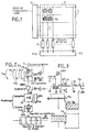
- FIG. 1 The general configuration of a line transfer photosensitive matrix is shown in FIG. 1. It comprises a network 10 of lines Li and columns Cj with, at the crossroads of each line and each column, a photosensitive detection element Pij.
- each photosensitive point of this line can provide, on the column conductor to which it is attached, a quantity of charges proportional to the integral of the light flux of illumination to which it was subjected during a determined period of integration time.
- the column conductors are connected to a reading circuit CL capable of receiving the charges of each column and of transforming them into a signal applied to a respective cell of an output shift register RDS; there are as many register boxes as output columns and these boxes are filled simultaneously by the signals representing the illumination of the different photosensitive points of that of the lines of the network 10 which has just been selected by the decoder 12.
- the read circuit which is considered according to the present invention is the circuit CL interposed between the columns of the network and the register.
- the RDS register is a charge transfer register and therefore the signal transferred to the boxes of the register will consist of a quantity of electric charges.
- the reading circuit CL is constituted by as many identical individual reading circuits CLj as there are columns Cj in the network 10.
- FIG. 2 schematically represents the main elements making it possible to implement the noise reduction method proposed here.
- the column Cj on which a quantity of charges Qs representing the useful signal to arrive, arrives, is connected to a charge injector constituted by a diode D1 and a passage grid Gp1 intended to authorize the passage of charges from the diode D1 to a region semiconductor which will be called in the following intermediate storage area.
- This intermediate storage area is located under a grid G1 which can also be called an intermediate storage grid.
- the intermediate storage grid is brought to a sufficiently positive potential to allow an accumulation of charges in the region which it covers.
- the passage gate Gp1 is connected to the output of an amplifier AMP1 of negative gain -G, the input of which is connected to the reading column Cj and therefore to the diode D1.
- the charge Qs is transferred under the intermediate storage grid G1 with a relatively limited thermal noise but which nevertheless includes the noise generated by the amplifier AMP1 itself.
- this drain region DR1 also allows the evacuation of the charges stored at the end of the reading cycle, when it is no longer needed.
- the operating cycle of the read circuit is broken down according to the invention into N stages, each comprising essentially three phases.
- the arrow F1a in FIG. 2 represents the path of the charges during the first phase of the first step of the reading cycle.
- the arrow F1b in FIG. 2 represents this development of the charge Qs *.
- replica charge of the charge Qs is meant a charge which may be equal to the charge Qs or in a known relationship with the charge Qs. In the preferred practical embodiment example, this is a charge equal to Qs and we will speak hereinafter of "duplication" of the charge Qs with regard to the development of the replica Qs *.
- the duplication of the charge Qs is done using an amplifier AMP2 according to an operating mode which will be explained later.
- the replica charge Qs * is stored in a region called "accumulation region" under a conductive grid M1.
- a third phase (restitution phase) of the first step represented by the arrow F1c in FIG. 2, the charge Qs which had been transferred in the opposite direction to the first phase is restored towards the diode D1 and the column Cj.
- This restitution is done by bringing the grid G1 to a strongly negative potential with respect to the potential of the column Cj.
- the first stage of the reading cycle thus ends.
- the second stage is a repetition of the phases of the first stage, namely first a phase (arrow F2a) of transfer from the column to the intermediate storage grid G1, then a phase of duplication (arrow F2b) of the transferred charge , and a phase for restoring the charge Qs to the column Cj.
- the "replica" charge formed in the second step is added, in the accumulation region under the gate M1, to that formed in the first step.
- the new replica charge Qs * is poured into the accumulation region under the gate M1 without having first removed the previous charge.
- the process is then continued by repeating each time the three phases of transfer, duplication, and restitution.
- the only difference is that the restitution phase is eliminated and that it is replaced by an evacuation phase towards the drain DR1 of the charge Qs which is no longer needed.
- the arrow Fnc in FIG. 2 represents this phase of evacuation to the drain DR1.
- the accumulation region must have a storage capacity which is all the more important as N is bigger.
- N the quantity of charges accumulated at the end of the reading cycle of a row of the matrix will be too large to be able to be transferred to the output register whose boxes are generally of small capacity for reasons of congestion and speed of operation.
- the arrows Fnd and Fne respectively represent the operations of transfer to the output register of the fraction of the charge accumulated during the n preceding steps, and of evacuation to a drain DR2 of the rest of the charge accumulated under the grid M1 since it is necessary to start from zero before recommencing a reading cycle.
- FIG. 3 represents on the one hand, in cross section, the structure allowing the transfer of the charge Qs from the column Cj to the intermediate storage area under the grid G1 , and on the other hand, below this section, the potential profiles in the various semiconductor regions of the structure.
- the structure is formed in a semiconductor substrate which is essentially of type p and that the potentials to be applied to the grids to allow a transfer of charges below this grid are positive potentials compared to the substrate.
- the type of substrate and the potentials could be reversed.
- the positive potentials are increasing downwards in accordance with a convention now classic in the field of charge transfer devices.
- the diode D1 the cathode of which consists of an N-type region 22 diffused in the semiconductor substrate 20.
- the cathode is connected to the column Cj and to the input of the amplifier AMP1 of negative gain -G.
- the output of the amplifier is connected to a gate Gp1 overhanging a region of substrate 24 immediately adjacent to the region of cathode 22.
- an auxiliary grid P1 is provided on the other side of the grid Gp1, brought to a fixed potential intermediate between the potentials of the passage grid Gp1 and of the intermediate storage grid G1, to limit the counter reaction of the potential of the grid G1 on the potential present in the region 24 under the grid Gp1.
- the drain DR1 is an N-type region diffused in the substrate and brought to a positive potential greater than that of the gate G1 at the time of evacuation.
- FIG. 4 represents a section of the structure serving for the duplication of the charge Qs stored under the intermediate storage grid G1, with, in correspondence with the different semiconductor regions of this structure, the successive potential profiles existing during the operation of duplication.
- the duplicator essentially comprises an AMP2 comparator, a first input of which is connected to the gate G1 under which the charge Qs is stored (affected by a transfer noise), and a second of which input is connected to a G2 grid under which the Qs * replica load must be generated.
- the replica charge Qs * is generated by a charge injector similar to the injector connected to the column Cj.
- This injector comprises an input diode D2 (analogous to D1), a passage gate Gp2 (analogous to Gp1), and possibly an auxiliary gate P2 (analogous to P1).
- the set D2, Gp2, P2, G2 is strictly identical to the set D1, Gp1, P1, G1, to obtain perfect symmetry of the components connected to the two inputs of the AMP2 comparator.
- the geometries of the grids G1 and G2 are in a given ratio to result in a replica charge Qs * in a known ratio different from 1 with Qs.
- the comparator inputs are also each connected to the source of a respective MOS transistor, T1 for the first input, T2 for the second, these transistors acting as switches and having their drains connected to a reference potential Vref and their gates connected to a control terminal which makes it possible to block the transistors for a time interval corresponding to the phase of duplication of charges.
- the transistors are turned on before the start of this interval.
- a passage grid P3 adjacent to the grid G2 makes it possible to ensure the transfer of the replica charge Qs * from the region located under the grid G2 to the region situated under the grid M1 mentioned with reference to FIG. 1.
- the charge Qs is duplicated as follows, illustrated by the potential levels represented respectively in dashed lines (at the start), in solid lines (during the transfer phase F1a or F2a, etc. from the diode D1 to the grid G1), and in dotted lines (during the actual duplication phase F1b, F1c, etc.).
- the grid P1 is at a low level, which retains the charge Qs on the column; the potential Vref is applied to the two comparator inputs; the latter is designed to have a characteristic like that of FIG. 5, that is to say that it has two stable states and provides a low potential Vgeb when the differential voltage between its inputs is negative or zero, and a potential high Vgeh when the input differential voltage is positive. The transition between these two states is as steep as possible.
- the differential voltage is zero and the comparator output level is therefore Vgeb. Furthermore, the cathode of the diode D2 is brought to a high level Vd2h; there is therefore no injection of charges under the grid G2.
- the transistors T1 and T2 are blocked and the gates G1 and G2 become floating; at the same time, the grid P1 is raised to a high level, which allows the transfer of Qs under the grid G1; by symmetry, an identical potential is preferably applied at the same time to the homologous grid P2; the potential of grid G1 decreases as charges accumulate under this grid; very quickly, the comparator switches and its output goes high Vgeh.
- the potential of the diode D2 is then brought to a low level Vd2b, which allows the injection of charges under the gate G2; as this injection progresses, the potential of the gate G2 decreases; when the potential of G2 reaches that of G1, the comparator switches back and blocks (by the grid Gp2) any additional transfer of charges from the diode D2 to the grid G2.
- the charge Qs * then present under the gate G2 is the same as the charge Qs under the gate G1 for the reasons of symmetry indicated above.
- FIG. 6 represents the whole of the structure making it possible to implement the invention, in top view and in cross section, and with in addition the potential profiles in the various semiconductor regions during the main operating phases.
- the blocking grid P4 On the other side of the grid M1, there is a blocking grid P4 and, on the other side of this grid P4, a grid M2 which is permanently brought to the same potential as the grid M1; the M2 grid participates in the accumulation of charges as long as the blocking gate P4 is at a higher potential than that of the metallizations M1 and M2, and the charges transferred from the gate G2 to the gate M1 are in fact distributed between the gates M1 and M2 in proportion of their respective surfaces.
- the blocking gate P4 is brought to a low potential (immediately before the start of the phase Fnd of FIG.
- the structure comprises, close to the metallization M1 and separated from it by a passage grid P6, the drain DR2 already mentioned in connection with FIG. 2; this passage grid is open during a final phase Fne to remove the charges remaining under the grid M1 at the end of the reading cycle.
- this load is then duplicated at the same time as the payload Qs. We find it multiplied by N in the sum of charges accumulated under the grids M1 and M2, and we still find it in the average transferred from the grid M2 to the output of the circuit.
- the drain drain DR1 adjacent to the grid G1 (FIG. 1) is replaced by a box of an auxiliary charge transfer register RA, separated from the grid G1 by a transfer gate in the same way as the drain DR1 was separated from the gate G1.
- This register permanently transports from one end to the other a load equal to the desired training load; this charge Q0 is injected at one end of the register.
- the charge Q0 is injected from the register under the gate G1 and from the gate G1 to the column Cj at each restitution phase F1c, F2c, etc.
Landscapes
- Engineering & Computer Science (AREA)
- Multimedia (AREA)
- Signal Processing (AREA)
- Solid State Image Pick-Up Elements (AREA)
- Transforming Light Signals Into Electric Signals (AREA)
Applications Claiming Priority (2)
| Application Number | Priority Date | Filing Date | Title |
|---|---|---|---|
| FR8800027 | 1988-01-05 | ||
| FR8800027A FR2625593B1 (fr) | 1988-01-05 | 1988-01-05 | Procede et circuit de lecture a faible bruit pour matrice photosensible a transfert de ligne |
Publications (2)
| Publication Number | Publication Date |
|---|---|
| EP0323924A1 true EP0323924A1 (de) | 1989-07-12 |
| EP0323924B1 EP0323924B1 (de) | 1992-11-11 |
Family
ID=9362069
Family Applications (1)
| Application Number | Title | Priority Date | Filing Date |
|---|---|---|---|
| EP89400008A Expired - Lifetime EP0323924B1 (de) | 1988-01-05 | 1989-01-03 | Leseverfahren und Schaltung mit niedrigem Geräusch für photosensitive Zeilentransfermatrix |
Country Status (5)
| Country | Link |
|---|---|
| US (1) | US4945420A (de) |
| EP (1) | EP0323924B1 (de) |
| JP (1) | JPH01217799A (de) |
| DE (1) | DE68903388T2 (de) |
| FR (1) | FR2625593B1 (de) |
Cited By (3)
| Publication number | Priority date | Publication date | Assignee | Title |
|---|---|---|---|---|
| CN101268683B (zh) * | 2005-08-01 | 2010-08-04 | 美光科技公司 | 包括双转换增益晶体管的成像装置、系统及控制成像、制造方法 |
| FR2951311A1 (fr) * | 2009-10-09 | 2011-04-15 | Trixell Sas | Procede de commande d'un dispositif photosensible |
| CN110121036A (zh) * | 2018-02-05 | 2019-08-13 | 联咏科技股份有限公司 | 影像感测装置与其黑电平修正方法及计算机可读媒体 |
Families Citing this family (4)
| Publication number | Priority date | Publication date | Assignee | Title |
|---|---|---|---|---|
| FR2731569B1 (fr) * | 1995-03-07 | 1997-04-25 | Thomson Tubes Electroniques | Dispositif de recopie de tension a grande linearite |
| US6469740B1 (en) * | 1997-02-04 | 2002-10-22 | Matsushita Electric Industrial Co., Ltd. | Physical quantity distribution sensor and method for driving the same |
| CA2679025A1 (en) * | 2007-02-23 | 2008-08-28 | Thermo Niton Analyzers Llc | Fast and precise time-resolved spectroscopy with linear sensor array |
| US20090122173A1 (en) * | 2007-11-13 | 2009-05-14 | William Emerson Tennant | Low noise readout apparatus and method for cmos image sensors |
Citations (1)
| Publication number | Priority date | Publication date | Assignee | Title |
|---|---|---|---|---|
| US3963942A (en) * | 1975-03-06 | 1976-06-15 | Bell Telephone Laboratories, Incorporated | Semiconductor charge transfer devices with dark current background cancellation |
Family Cites Families (5)
| Publication number | Priority date | Publication date | Assignee | Title |
|---|---|---|---|---|
| EP0115225B1 (de) * | 1982-12-21 | 1987-05-06 | Thomson-Csf | Verfahren zur Abtastung eines nach dem Zwischenspaltenprinzips wirkenden Bildsensors und Anordnung zur Durchführung des Verfahrens |
| FR2557372B1 (fr) * | 1983-12-27 | 1986-04-11 | Thomson Csf | Procede d'ebasage d'un dispositif photosensible a l'etat solide |
| FR2580883B1 (fr) * | 1985-04-19 | 1987-05-22 | Thomson Csf | Dispositif de lecture par transfert de ligne avec contre-reaction |
| FR2608340B1 (fr) * | 1986-12-16 | 1989-02-17 | Thomson Csf | Circuit de lecture d'un dispositif photosensible a transfert de ligne, dispositif photosensible a transfert de ligne comportant un tel circuit et procede de lecture d'un tel dispositif |
| US4752829A (en) * | 1986-12-29 | 1988-06-21 | Fairchild Weston Systems, Inc. | Multipacket charge transfer image sensor and method |
-
1988
- 1988-01-05 FR FR8800027A patent/FR2625593B1/fr not_active Expired - Lifetime
- 1988-12-29 JP JP63335683A patent/JPH01217799A/ja active Pending
-
1989
- 1989-01-03 DE DE8989400008T patent/DE68903388T2/de not_active Expired - Fee Related
- 1989-01-03 EP EP89400008A patent/EP0323924B1/de not_active Expired - Lifetime
- 1989-01-04 US US07/293,469 patent/US4945420A/en not_active Expired - Lifetime
Patent Citations (1)
| Publication number | Priority date | Publication date | Assignee | Title |
|---|---|---|---|---|
| US3963942A (en) * | 1975-03-06 | 1976-06-15 | Bell Telephone Laboratories, Incorporated | Semiconductor charge transfer devices with dark current background cancellation |
Non-Patent Citations (2)
| Title |
|---|
| PROCEEDINGS OF 5TH INTERNATIONAL CONFERENCE ON CHARGE-COUPLED DEVICES, septembre 1979, pages 33-39, J. MAVOR, University of Edinburgh; S. IWASA et al.: "Mosaic CCD multiplexer for pyroelectric hybrid focal plane" * |
| RCA REVIEW, vol. 40, no. 3, septembre 1979, pages 241-277, Princeton, US; W.F. KOSONOCKY et al.: "Low-loss charge-coupled device" * |
Cited By (5)
| Publication number | Priority date | Publication date | Assignee | Title |
|---|---|---|---|---|
| CN101268683B (zh) * | 2005-08-01 | 2010-08-04 | 美光科技公司 | 包括双转换增益晶体管的成像装置、系统及控制成像、制造方法 |
| FR2951311A1 (fr) * | 2009-10-09 | 2011-04-15 | Trixell Sas | Procede de commande d'un dispositif photosensible |
| WO2011042204A3 (fr) * | 2009-10-09 | 2011-06-16 | Trixell Sas | Procede pour la reduction du bruit dans le signal d'image d'un dispositif photosensible |
| US8994853B2 (en) | 2009-10-09 | 2015-03-31 | Commissariat A L'energie Atomique Et Aux Energies Alternatives | Method for controlling a light-sensitive device |
| CN110121036A (zh) * | 2018-02-05 | 2019-08-13 | 联咏科技股份有限公司 | 影像感测装置与其黑电平修正方法及计算机可读媒体 |
Also Published As
| Publication number | Publication date |
|---|---|
| FR2625593B1 (fr) | 1990-05-04 |
| DE68903388D1 (de) | 1992-12-17 |
| DE68903388T2 (de) | 1993-03-25 |
| JPH01217799A (ja) | 1989-08-31 |
| FR2625593A1 (fr) | 1989-07-07 |
| EP0323924B1 (de) | 1992-11-11 |
| US4945420A (en) | 1990-07-31 |
Similar Documents
| Publication | Publication Date | Title |
|---|---|---|
| EP0364314B1 (de) | Verfahren zum Lesen von lichtempfindlichen Zellen mit zwei in Reihe angeordneten Dioden und mit entgegenwirkenden Durchlassrichtungen | |
| EP0153251B1 (de) | Bildaufnahmevorrichtung mit stabförmiger multilinearer Ladungsverschiebungsanordnung | |
| EP0168267A1 (de) | Aus mehreren Zeilen bestehende ladungsgekoppelte Sensoranordnung und Abtastverfahren | |
| EP0181664A1 (de) | Synchronisierter Komparator | |
| EP0474550A1 (de) | Bilddetektor mit Grossformat-Pixels | |
| EP0323924B1 (de) | Leseverfahren und Schaltung mit niedrigem Geräusch für photosensitive Zeilentransfermatrix | |
| EP0234968B1 (de) | Leseverfahren eines photoempfindlichen Elements, bestehend aus einer Photodiode und einer Kapazität | |
| EP0324677B1 (de) | Photoempfindliche Matrix mit drei Dioden pro Punkt ohne Rückstellung | |
| EP0006053B1 (de) | Differenzbildungsvorrichtung mit Ladungskopplung; Filter und Verzögerungsleitung mit einer solchen Vorrichtung | |
| EP0230809B1 (de) | Wärmebildkamera mit Parallelabtastung | |
| EP0182679B1 (de) | Photoempfindliche Zwischenspaltanordnung mit zurückgekoppeltem Verstärker | |
| EP0148086B1 (de) | Hintergrundladungsbeseitigung in einer lichtempfindlichen Festkörperanordnung | |
| EP0068947B1 (de) | Lichtdetektoreinheit, entsprechender Leser mit Ladungsübertragung und Bildaufnahmeeinrichtung die eine solche Einheit enthält | |
| EP0958545B1 (de) | Integratorschaltung von photoerzeugten ladungen mit verbesserter linearität | |
| EP0325524B1 (de) | Ladungstransferspeicher und Verfahren zur Herstellung desselben | |
| FR2511545A1 (fr) | Dispositif semi-conducteur comportant un dispositif a couplage de charges a quatre phases | |
| EP0012667B1 (de) | Verfahren zum Filtern eines elektrischen Signals durch Ladungsübertragung in einem Halbleiter und Filter mit geschalteten Kondensatoren, das dieses Verfahren verwendet | |
| FR2558670A1 (fr) | Perfectionnement aux dispositifs photosensibles a l'etat solide | |
| EP0009438A1 (de) | Dynamisches Speicherelement mit Ladungsübertragung und Anwendung in einem Schieberegister | |
| EP0021908B1 (de) | Phasenumkehrschaltung mit Ladungsübertragung und Differenzverstärker mit solch einer Schaltung | |
| FR2549999A1 (fr) | Cellule de memoire du type ram comprenant un element de memoire non volatil electriquement programmable | |
| EP0478440B1 (de) | Vorladeschaltung um einen Speicher zu lesen | |
| EP0329518B1 (de) | Ladungslese-Einrichtung für einen linearen Photosensor mit einer Anti-überstrahlungseinrichtung mit Linienstruktur | |
| EP0332499B1 (de) | Schneller Komparator mit in zwei Phasen arbeitender Ausgangsstufe | |
| EP0275740B1 (de) | Ausleseschaltung für eine lichtempfindliche Zeilenübertragungsanordnung, lichtempfindliche Zeilenübertragungsanordnung mit einer solchen Schaltung und Ausleseverfahren einer solchen Anordnung |
Legal Events
| Date | Code | Title | Description |
|---|---|---|---|
| PUAI | Public reference made under article 153(3) epc to a published international application that has entered the european phase |
Free format text: ORIGINAL CODE: 0009012 |
|
| AK | Designated contracting states |
Kind code of ref document: A1 Designated state(s): DE FR GB NL |
|
| 17P | Request for examination filed |
Effective date: 19890826 |
|
| 17Q | First examination report despatched |
Effective date: 19911002 |
|
| GRAA | (expected) grant |
Free format text: ORIGINAL CODE: 0009210 |
|
| AK | Designated contracting states |
Kind code of ref document: B1 Designated state(s): DE FR GB NL |
|
| PG25 | Lapsed in a contracting state [announced via postgrant information from national office to epo] |
Ref country code: GB Effective date: 19921111 |
|
| REF | Corresponds to: |
Ref document number: 68903388 Country of ref document: DE Date of ref document: 19921217 |
|
| GBV | Gb: ep patent (uk) treated as always having been void in accordance with gb section 77(7)/1977 [no translation filed] |
Effective date: 19921111 |
|
| PLBE | No opposition filed within time limit |
Free format text: ORIGINAL CODE: 0009261 |
|
| STAA | Information on the status of an ep patent application or granted ep patent |
Free format text: STATUS: NO OPPOSITION FILED WITHIN TIME LIMIT |
|
| 26N | No opposition filed | ||
| PGFP | Annual fee paid to national office [announced via postgrant information from national office to epo] |
Ref country code: FR Payment date: 20030110 Year of fee payment: 15 |
|
| PGFP | Annual fee paid to national office [announced via postgrant information from national office to epo] |
Ref country code: DE Payment date: 20030116 Year of fee payment: 15 |
|
| PGFP | Annual fee paid to national office [announced via postgrant information from national office to epo] |
Ref country code: NL Payment date: 20030130 Year of fee payment: 15 |
|
| PG25 | Lapsed in a contracting state [announced via postgrant information from national office to epo] |
Ref country code: NL Free format text: LAPSE BECAUSE OF NON-PAYMENT OF DUE FEES Effective date: 20040801 |
|
| PG25 | Lapsed in a contracting state [announced via postgrant information from national office to epo] |
Ref country code: DE Free format text: LAPSE BECAUSE OF NON-PAYMENT OF DUE FEES Effective date: 20040803 |
|
| PG25 | Lapsed in a contracting state [announced via postgrant information from national office to epo] |
Ref country code: FR Free format text: LAPSE BECAUSE OF NON-PAYMENT OF DUE FEES Effective date: 20040930 |
|
| NLV4 | Nl: lapsed or anulled due to non-payment of the annual fee |
Effective date: 20040801 |
|
| REG | Reference to a national code |
Ref country code: FR Ref legal event code: ST |