EP0324123A2 - Procédé et dispositif pour la fabrication d'un support d'information magnéto-optique enregistrable et/ou effaçable - Google Patents
Procédé et dispositif pour la fabrication d'un support d'information magnéto-optique enregistrable et/ou effaçable Download PDFInfo
- Publication number
- EP0324123A2 EP0324123A2 EP88120847A EP88120847A EP0324123A2 EP 0324123 A2 EP0324123 A2 EP 0324123A2 EP 88120847 A EP88120847 A EP 88120847A EP 88120847 A EP88120847 A EP 88120847A EP 0324123 A2 EP0324123 A2 EP 0324123A2
- Authority
- EP
- European Patent Office
- Prior art keywords
- cathode
- magnetron
- substrate
- magnetic
- compensation temperature
- Prior art date
- Legal status (The legal status is an assumption and is not a legal conclusion. Google has not performed a legal analysis and makes no representation as to the accuracy of the status listed.)
- Withdrawn
Links
- 238000000034 method Methods 0.000 title claims abstract description 16
- 238000004519 manufacturing process Methods 0.000 title claims description 9
- 230000005291 magnetic effect Effects 0.000 claims abstract description 62
- 239000000758 substrate Substances 0.000 claims abstract description 27
- 239000000126 substance Substances 0.000 claims abstract description 22
- 239000000203 mixture Substances 0.000 claims abstract description 19
- 230000008859 change Effects 0.000 claims abstract description 13
- 239000000969 carrier Substances 0.000 claims abstract description 5
- 229910045601 alloy Inorganic materials 0.000 claims description 36
- 239000000956 alloy Substances 0.000 claims description 36
- 238000004544 sputter deposition Methods 0.000 claims description 20
- 150000003624 transition metals Chemical group 0.000 claims description 15
- 150000002910 rare earth metals Chemical group 0.000 claims description 9
- 230000008569 process Effects 0.000 claims description 7
- 239000010409 thin film Substances 0.000 claims description 6
- 230000033228 biological regulation Effects 0.000 claims description 5
- 230000003628 erosive effect Effects 0.000 claims description 5
- XEEYBQQBJWHFJM-UHFFFAOYSA-N Iron Chemical compound [Fe] XEEYBQQBJWHFJM-UHFFFAOYSA-N 0.000 claims description 4
- 239000000463 material Substances 0.000 claims description 4
- 229910052771 Terbium Inorganic materials 0.000 claims description 3
- 229910017052 cobalt Inorganic materials 0.000 claims description 3
- 239000010941 cobalt Substances 0.000 claims description 3
- GUTLYIVDDKVIGB-UHFFFAOYSA-N cobalt atom Chemical compound [Co] GUTLYIVDDKVIGB-UHFFFAOYSA-N 0.000 claims description 3
- 230000001105 regulatory effect Effects 0.000 claims description 3
- GZCRRIHWUXGPOV-UHFFFAOYSA-N terbium atom Chemical compound [Tb] GZCRRIHWUXGPOV-UHFFFAOYSA-N 0.000 claims description 3
- 229910002058 ternary alloy Inorganic materials 0.000 claims description 3
- 229910052581 Si3N4 Inorganic materials 0.000 claims description 2
- 229910002056 binary alloy Inorganic materials 0.000 claims description 2
- 238000001514 detection method Methods 0.000 claims description 2
- 238000005259 measurement Methods 0.000 claims description 2
- 229910052751 metal Inorganic materials 0.000 claims description 2
- 239000002184 metal Substances 0.000 claims description 2
- 229910002059 quaternary alloy Inorganic materials 0.000 claims description 2
- 229910052742 iron Inorganic materials 0.000 claims 1
- 238000001755 magnetron sputter deposition Methods 0.000 abstract description 2
- 239000010410 layer Substances 0.000 description 30
- 230000005415 magnetization Effects 0.000 description 14
- 229910052723 transition metal Inorganic materials 0.000 description 14
- 230000006399 behavior Effects 0.000 description 10
- 229910052761 rare earth metal Inorganic materials 0.000 description 7
- 230000008901 benefit Effects 0.000 description 5
- 238000009826 distribution Methods 0.000 description 5
- 230000010287 polarization Effects 0.000 description 5
- 230000000694 effects Effects 0.000 description 4
- 230000005293 ferrimagnetic effect Effects 0.000 description 4
- 230000005294 ferromagnetic effect Effects 0.000 description 4
- 230000006870 function Effects 0.000 description 4
- 239000007789 gas Substances 0.000 description 4
- 230000005374 Kerr effect Effects 0.000 description 3
- 238000013500 data storage Methods 0.000 description 3
- 239000010408 film Substances 0.000 description 3
- 230000004907 flux Effects 0.000 description 3
- 230000007774 longterm Effects 0.000 description 3
- 230000015654 memory Effects 0.000 description 3
- 239000002245 particle Substances 0.000 description 3
- 239000007858 starting material Substances 0.000 description 3
- XKRFYHLGVUSROY-UHFFFAOYSA-N Argon Chemical compound [Ar] XKRFYHLGVUSROY-UHFFFAOYSA-N 0.000 description 2
- 239000011248 coating agent Substances 0.000 description 2
- 238000000576 coating method Methods 0.000 description 2
- 238000001816 cooling Methods 0.000 description 2
- 229910052746 lanthanum Inorganic materials 0.000 description 2
- 239000002346 layers by function Substances 0.000 description 2
- 229910052745 lead Inorganic materials 0.000 description 2
- 230000003287 optical effect Effects 0.000 description 2
- 230000005693 optoelectronics Effects 0.000 description 2
- 238000003860 storage Methods 0.000 description 2
- 229910052719 titanium Inorganic materials 0.000 description 2
- 229910002546 FeCo Inorganic materials 0.000 description 1
- 238000005299 abrasion Methods 0.000 description 1
- 229910052786 argon Inorganic materials 0.000 description 1
- 238000010276 construction Methods 0.000 description 1
- 238000005260 corrosion Methods 0.000 description 1
- 230000007797 corrosion Effects 0.000 description 1
- 239000013078 crystal Substances 0.000 description 1
- 230000007423 decrease Effects 0.000 description 1
- 230000003247 decreasing effect Effects 0.000 description 1
- 238000012217 deletion Methods 0.000 description 1
- 230000037430 deletion Effects 0.000 description 1
- 230000001687 destabilization Effects 0.000 description 1
- 238000010586 diagram Methods 0.000 description 1
- 238000006073 displacement reaction Methods 0.000 description 1
- 239000012212 insulator Substances 0.000 description 1
- 230000003993 interaction Effects 0.000 description 1
- 230000003647 oxidation Effects 0.000 description 1
- 238000007254 oxidation reaction Methods 0.000 description 1
- 230000005298 paramagnetic effect Effects 0.000 description 1
- 239000000843 powder Substances 0.000 description 1
- 238000001552 radio frequency sputter deposition Methods 0.000 description 1
- 230000000717 retained effect Effects 0.000 description 1
- 230000035945 sensitivity Effects 0.000 description 1
- 238000005245 sintering Methods 0.000 description 1
- 230000002269 spontaneous effect Effects 0.000 description 1
- 239000013077 target material Substances 0.000 description 1
- 238000001771 vacuum deposition Methods 0.000 description 1
Images

Classifications
-
- G—PHYSICS
- G11—INFORMATION STORAGE
- G11B—INFORMATION STORAGE BASED ON RELATIVE MOVEMENT BETWEEN RECORD CARRIER AND TRANSDUCER
- G11B5/00—Recording by magnetisation or demagnetisation of a record carrier; Reproducing by magnetic means; Record carriers therefor
- G11B5/84—Processes or apparatus specially adapted for manufacturing record carriers
- G11B5/851—Coating a support with a magnetic layer by sputtering
-
- C—CHEMISTRY; METALLURGY
- C23—COATING METALLIC MATERIAL; COATING MATERIAL WITH METALLIC MATERIAL; CHEMICAL SURFACE TREATMENT; DIFFUSION TREATMENT OF METALLIC MATERIAL; COATING BY VACUUM EVAPORATION, BY SPUTTERING, BY ION IMPLANTATION OR BY CHEMICAL VAPOUR DEPOSITION, IN GENERAL; INHIBITING CORROSION OF METALLIC MATERIAL OR INCRUSTATION IN GENERAL
- C23C—COATING METALLIC MATERIAL; COATING MATERIAL WITH METALLIC MATERIAL; SURFACE TREATMENT OF METALLIC MATERIAL BY DIFFUSION INTO THE SURFACE, BY CHEMICAL CONVERSION OR SUBSTITUTION; COATING BY VACUUM EVAPORATION, BY SPUTTERING, BY ION IMPLANTATION OR BY CHEMICAL VAPOUR DEPOSITION, IN GENERAL
- C23C14/00—Coating by vacuum evaporation, by sputtering or by ion implantation of the coating forming material
- C23C14/22—Coating by vacuum evaporation, by sputtering or by ion implantation of the coating forming material characterised by the process of coating
- C23C14/34—Sputtering
- C23C14/35—Sputtering by application of a magnetic field, e.g. magnetron sputtering
-
- G—PHYSICS
- G11—INFORMATION STORAGE
- G11B—INFORMATION STORAGE BASED ON RELATIVE MOVEMENT BETWEEN RECORD CARRIER AND TRANSDUCER
- G11B11/00—Recording on or reproducing from the same record carrier wherein for these two operations the methods are covered by different main groups of groups G11B3/00 - G11B7/00 or by different subgroups of group G11B9/00; Record carriers therefor
- G11B11/10—Recording on or reproducing from the same record carrier wherein for these two operations the methods are covered by different main groups of groups G11B3/00 - G11B7/00 or by different subgroups of group G11B9/00; Record carriers therefor using recording by magnetic means or other means for magnetisation or demagnetisation of a record carrier, e.g. light induced spin magnetisation; Demagnetisation by thermal or stress means in the presence or not of an orienting magnetic field
- G11B11/105—Recording on or reproducing from the same record carrier wherein for these two operations the methods are covered by different main groups of groups G11B3/00 - G11B7/00 or by different subgroups of group G11B9/00; Record carriers therefor using recording by magnetic means or other means for magnetisation or demagnetisation of a record carrier, e.g. light induced spin magnetisation; Demagnetisation by thermal or stress means in the presence or not of an orienting magnetic field using a beam of light or a magnetic field for recording by change of magnetisation and a beam of light for reproducing, i.e. magneto-optical, e.g. light-induced thermomagnetic recording, spin magnetisation recording, Kerr or Faraday effect reproducing
- G11B11/10582—Record carriers characterised by the selection of the material or by the structure or form
- G11B11/10586—Record carriers characterised by the selection of the material or by the structure or form characterised by the selection of the material
-
- H—ELECTRICITY
- H01—ELECTRIC ELEMENTS
- H01J—ELECTRIC DISCHARGE TUBES OR DISCHARGE LAMPS
- H01J37/00—Discharge tubes with provision for introducing objects or material to be exposed to the discharge, e.g. for the purpose of examination or processing thereof
- H01J37/32—Gas-filled discharge tubes
- H01J37/34—Gas-filled discharge tubes operating with cathodic sputtering
- H01J37/3402—Gas-filled discharge tubes operating with cathodic sputtering using supplementary magnetic fields
- H01J37/3405—Magnetron sputtering
Definitions
- the invention relates to a method and a device for producing magneto-optical, storable and / or erasable data carriers using various chemical substances, these substances being applied as layers to a substrate by means of a magnetron sputter system.
- Data storage on the basis of magneto-optical phenomena combines the advantages of magnetic data storage, which consist in the fact that data can be erased and rewritten on the same carrier, with the advantages of purely optical data storage, which, for. B. in the avoidance of unwanted data deletions by crashing the header on the disk.
- magneto-optical memories which are of the order of 5 x 108 bit / cm2 and enable the production of gigabyte storage disks.
- magneto-optical memory With this magneto-optical memory, use is made of the fact that polarized light experiences a rotation of its polarization plane when passing through a magnetic field (Faraday effect) and when it is reflected on a ferromagnetic surface (magneto-optical Kerr effect).
- the size of the rotation of the polarization plane is for a given Material a monotonous function of magnetization.
- a magnetic layer is sputtered on, which mainly consists of binary, ternary or quaternary alloys from the elements of the rare earth group (59Pr -70Yb) and the group of transition metals (26Fe -28Ni) (Mark H Kryder, J. Vac. Sci.
- the angle through which the light polarization direction is rotated in one direction or the other, depending on the orientation of the magnetization of the reflecting region, should be large.
- the layer is heated up to the area of the compensation point of the ferrimagnetic system with a laser and thus an orientation is impressed on it in a magnetic field.
- Laser light of significantly lower intensity, but instead linear polarization, is used to read this information.
- Its orientation is rotated due to the magneto-optical Kerr effect.
- the direction of rotation is determined with an analyzer; it contains the stored information (Hans-Gerd Severin: Sputtering, The Generation of Thin Layers, Physics in Our Time, 17th year 1986, pp. 71 to 79, especially pp. 77/78).
- metal layers or dielectric layers e.g. B. Al, AlN or Si3N4.
- the starting materials of the alloys that is, the rare earths and the transition metals
- the alloys of these starting materials have a ferrimagnetic order, that is to say the rare earths and transition metals which are each ferromagnetically ordered, couple to one another antiferromagnetically.
- the magnetization behavior of the alloy layers corresponds to that of soft magnets. In addition to a high squareness ( ⁇ 1), they have a strong magnetic anisotropy of (k u ⁇ 106 erg / cm3) perpendicular to the layer surface.
- Further parameters for the magnetic behavior of thin layers of rare earth and transition metals are the coercive field strengths H c, for example at room temperature, the compensation temperature T comp and the Curie temperature T c .
- the coercive field strength is defined here as the negative field strength H c which brings the magnetic flux density B back to zero.
- the Curie temperature T c is the temperature at which the ferromagnetic properties of a substance disappear.
- the compensation temperature T comp is the temperature at which the magnetization of an alloy is zero, due to the addition of the positive magnetization of one substance of the alloy with the negative magnetization of the other substance of the alloy. At the compensation temperature T comp , the magnetization also completely disappears, but in contrast to the Curie temperature, the magnetic order of the individual substances is retained.
- rare earth and transition metals differ both in terms of the direction of magnetization and in the temperature dependence of the amount of magnetization, a typical temperature dependence of the magnetization of the overall alloy system arises. It is therefore very important to determine or determine the proportion of rare earth and transition metals within an alloy.
- Sputtering systems are already known in which targets composed of plates of the individual elements, so-called mosaic targets, are used in order to be able to determine the rare earth and transition metal content in the alloy layers.
- mosaic targets targets
- the particle emission characteristics of the racetracks change with different effects on the distribution of the Individual elements in the plasma. These effects lead to fluctuations or long-term drift of the functional layers produced.
- a disadvantage of this known method is that changes in the process pressure during magnetron sputtering lead to undesirable changes in the microstructure of the thin alloy layers.
- the specific rates for diode sputtering are comparatively low and very high target voltages are required.
- the creation of a substrate bias in a production plant is not technically easy to solve and in the case of an RF bias often leads to a destabilization of the processes. Since high concentrations of Ar atoms are also incorporated into the layers, the magnetic properties of the alloy layers obtained in this way are not stable over the long term.
- a sputtering cathode which is suitable for both magnetic and non-magnetic target materials, allows the coating of large areas while the substrates are in transit, leads to a very uniform layer thickness distribution and can nevertheless be operated with only a single power supply (EP 0 253 344 A2).
- This sputtering cathode has at least three magnet units lying one inside the other and has a mechanical adjusting device by means of which the magnetic flux between a magnet yoke and at least one magnet unit can be changed relative to the magnetic flux between the magnet yoke and the other units.
- a device for improving the electro-optical effect of a ferroelectric thin film composed of oxides of Pb, Ti and La is also known, the molar ratio of Pb to Ti being set within a specific range (Patents Abstracts of Japan, June 8, 1984, Vol. 8, No. 122, JP-OS 59-35098).
- powdered oxides of Pb, Ti and La are mixed together, calcined and sputtered by using the powder as a target to form a thin film on a substrate.
- the molar ratio of Pb to Ti is preferably 0.65 ⁇ Pb / Ti ⁇ 0.90.
- the electro-optical effect of the resulting ferroelectric thin single crystal film is thereby improved and can be used as a light switching material.
- the object of the invention is to precisely determine the proportions of different substances which are applied to a substrate using a magnetron system within an alloy.
- the invention also takes advantage of the fact that system geometry and different angular distributions of the elements in alloy targets in the sputtering process can lead to changes in the film composition by deliberately changing the composition values and thus the magnetic properties in a magnetic thin film. This is done on the basis of the detection of the magnetic properties immediately after the layer has been produced and a corresponding regulation.
- the interaction of aperture diaphragm and field strength in the magnetron is also advantageous in the invention.
- Another advantage of the invention is that the target is composed uniformly over its entire surface, that is, it does not have to be a ring target made of another material, which extends the life of the target.
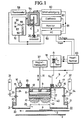
- the cathode sputtering device 1 shows a magnetron cathode sputtering device 1, which is arranged opposite a substrate carrier 2, behind which a shield 3 is located. A substrate 4 to be coated is arranged on the substrate carrier 2.
- the cathode sputtering device 1 has a cathode device 5, which in turn has the actual sputtering or target cathode 6 and a cathode trough 7.
- the z. B. consists of an alloy of rare earths and transition metals, and in the cathode trough 7 permanent magnets 8, 9, 10 are provided, which are completed by a common yoke 2.
- a cooling channel 27 for cooling the cathode is provided on the bottom of the cathode tub 7.
- the magnets 8, 9, 10 on the yoke plate 12 are not cooled. You are in the surrounding atmosphere.
- the cathode trough 7 has a flange-shaped edge 13 which, with the interposition of an insulator 14 in the form of an O-ring, is connected to the ceiling 15 of a cathode chamber 28 which is at ground potential.
- One or more pumps 16, 17 are also connected to this ceiling 15 via large suction cross sections, which constantly empty the cathode chamber 28.
- the cathode tub 7 is electrically connected to the negative pole of a controllable DC voltage source 18, which supplies a DC voltage of approximately 0 to 1000 volts.
- Opposite the sputtering cathode 6 are two legs 21, 22 standing perpendicular to one another, one leg 21 being connected to a side wall 24 of the cathode chamber 28 via an electrically conductive connecting piece 23. The legs 21, 22 are thus also at ground potential.
- the legs 22 also have an opening 25 with the diameter S and thus act as an aperture.
- This aperture is z. B. interchangeable via the connector 23 or adjustable in terms of their diameter S, which is not shown in FIG. 1.
- the size S of the aperture 25 has an influence on the composition of the sputtered alloy.
- a presetting across the width S of the aperture diaphragm is required in order to generate uniform compensation temperatures over the entire length of the cathode and transversely to the transport direction. This default setting is not changed during operation.
- the gas required for the process comes from gas sources 31, 32 and reaches the cathode chamber 28 via control valves 33, 34. Argon, for example, can be used as the gas.
- the magnetic field 40 of the magnetron 1 which consists of the two subfields 41, 42, is changed.
- the field 40 of the magnetron is changed by changing the position of the permanent magnets 8, 9, 10 by means of a rod or the like relative to the surface of the target 6, but not in its geometry.
- the magnetic field 40 of the cathode 7 determines the voltage that is applied to the cathode 7 by the voltage source 18.
- the magnetic properties of the applied layers are continuously measured using a magnetometer.
- a special Kerr magnetometer 51, 58 is provided for the measurement of these properties, which is shown in the upper part of FIG. 1 for the sake of clarity, although it is arranged in the vicinity of the substrate carrier 2.
- the substrate carrier 2 with the substrate 4 is shown again in the upper part of FIG. 1.
- the Kerr magnetometer consists of a head 51, a thermometer 58 and a measuring magnet 54.
- This Kerr magnetometer measures the Kerr magnetization curve of the alloy layer produced on the substrate 4 at point 53.
- the carrier 2 is moved by two drive rollers 20, 26.
- the Kerr magnetometer 51, 58 is controlled by a personal computer 59 which changes the magnetic field of the measuring magnet 54 in preselectable steps via a power supply 60.
- the personal computer 59 registers the rotation of polarized light originating from the laser 50, which is reflected on a sample surface of the carrier 2. This registration is carried out with the aid of a Woolaston prism 55 and two photodiodes 56, 57.
- Electronics 62 determine the degree of polarization of the measuring light from the electrical signal of these two diodes 56, 57. Since the sample temperature at point 53 and the optical thermometer 58 is also determined at the same time, the personal computer 59 is able to determine the compensation temperature from a fit for the coercive field strength.
- the value for the compensation temperature is fed to a main computer 63, which compares the current value for T comp with a predetermined value desired for the respective product.
- the regulation then takes place with the aid of the magnetic lifting system, which is known, for example, from DE-OS 30 47 113 or US Pat. No. 4,426,264, the dependencies shown in FIGS. 3, 4, 5 described below being taken into account, ie the magnetic lifting system 37 moves the cathode 6 to the corresponding voltage by changing the position of the magnets 8, 9, 10.
- the target voltage is a measure of the strength of the magnetic field on the target surface.
- the task of the electronics 62 is to amplify the signals of the two photodiodes 56, 57 in the measuring head 51 and the size to form, which is a direct measure of the torsion of the sputtered layer, which the personal computer 59 calculates.
- the main computer 63 controls the entire coating system, the control of the cathode voltage via the magnetic lifting system and the control of the cathode power density via the sputtering power supply being particularly important.
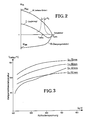
- Curve A shows the behavior of the rare earths. It can be seen from this illustration that the magnetic moment of the rare earths assumes a positive value M SE at low temperatures, which is very high, and that this value decreases continuously with increasing temperature in order to assume the value zero at the Curie temperature T curie .
- the coercive field strength H c has a pole point, ie it assumes the value infinity on both sides of T comp , since at this temperature the magnetization disappears, the energy density M s . H c remains. If this compensation temperature T comp is brought to the value of the ambient temperature, this means that no information can be deleted at ambient temperature. This is a desirable condition, which is why it makes sense to choose the composition of the alloy so that T comp corresponds to the ambient temperature.
- the compensation temperature shifts by 40 ° C or the Curie temperature by 8 ° C.
- the sputtering behavior of magneto-optical targets can be interpreted to mean that the individual elements of the target alloy have different angular distributions in front of the magnetron's racetrack.
- the rare earth sputter particles are more extended laterally or more concentrated in the center than the transition metals. If the surrounding geometry of the cathode is adapted accordingly, outer parts of the particle flow to the substrate can be hidden. Since a change in the magnetic field of the cathode changes the plasma geometry, the hidden part can be controlled. This is the basis of the control principle according to the invention, since the layer composition varies accordingly.
- FIG. 3 shows the dependence of the compensation temperature T comp for a Tb 0.24 Fe 0.68 Co 0.08 target on the target or cathode voltage U K , the various curves showing the widths S of the opening 25 (FIG 1) represent. It can be seen from this illustration that the compensation temperature T comp increases with increasing target voltage and with decreasing gap width. A fresh target is always assumed. 3 also shows that a change in the magnetic field of the magnetron cathode 6 leads to smaller field strengths, which is indicated by higher cathode voltages. This in turn leads to an increase in the proportion of rare earth in the alloy produced.
- the compensation temperature of the alloy layers produced can be roughly adjusted by changing this aperture diaphragm width S, while the change in the magnetic field enables finer displacements. For a given sputtering or cathode voltage, there is a different compensation temperature for each gap width. If the normal control range is exhausted, it is possible to switch to a different aperture width S switch. Since the cathode voltage is a measure of the strength of the magnetic field on the target surface, the voltage axis of FIG. 3 can also be understood as a magnetic field strength axis.
- FIG. 4 shows the dependence of the compensation temperature T comp on the cathode voltage U K with a constant gap S of the shield 22 and with an eroded target.
- the target erosion is assumed to be 50%. It can be seen from this that the dependence of the compensation temperature T comp on the cathode voltage U K changes in the course of the target erosion. In contrast to the illustration in FIG. 3, this is not always a fresh target. The practical consequence of this is that production actually has to be continuously measured and readjusted. Compared to the regulation based only on the current cathode voltage, the target life can be extended considerably, which is very important because magneto-optical targets are very expensive.
- a diagram or a computer can be used to determine in which way the cathode voltage has to be changed, which in turn can be adjusted via the controller of the magnet spacing happens. It is a closed control loop.
Landscapes
- Chemical & Material Sciences (AREA)
- Engineering & Computer Science (AREA)
- Physics & Mathematics (AREA)
- Plasma & Fusion (AREA)
- Analytical Chemistry (AREA)
- Chemical Kinetics & Catalysis (AREA)
- Materials Engineering (AREA)
- Mechanical Engineering (AREA)
- Metallurgy (AREA)
- Organic Chemistry (AREA)
- Physical Vapour Deposition (AREA)
- Thin Magnetic Films (AREA)
Applications Claiming Priority (2)
| Application Number | Priority Date | Filing Date | Title |
|---|---|---|---|
| DE3800449 | 1988-01-09 | ||
| DE3800449A DE3800449A1 (de) | 1988-01-09 | 1988-01-09 | Verfahren und einrichtung zur herstellung magnetooptischer, speicher- und loeschfaehiger datentraeger |
Publications (2)
| Publication Number | Publication Date |
|---|---|
| EP0324123A2 true EP0324123A2 (fr) | 1989-07-19 |
| EP0324123A3 EP0324123A3 (fr) | 1990-11-07 |
Family
ID=6345017
Family Applications (1)
| Application Number | Title | Priority Date | Filing Date |
|---|---|---|---|
| EP19880120847 Withdrawn EP0324123A3 (fr) | 1988-01-09 | 1988-12-14 | Procédé et dispositif pour la fabrication d'un support d'information magnéto-optique enregistrable et/ou effaçable |
Country Status (4)
| Country | Link |
|---|---|
| US (1) | US4927513A (fr) |
| EP (1) | EP0324123A3 (fr) |
| JP (1) | JPH01290144A (fr) |
| DE (1) | DE3800449A1 (fr) |
Cited By (1)
| Publication number | Priority date | Publication date | Assignee | Title |
|---|---|---|---|---|
| DE10119533A1 (de) * | 2001-04-12 | 2002-10-24 | Siemens Ag | Verfahren zur Steuerung eines Plasmas in einem Magnetron-Sputterprozess |
Families Citing this family (26)
| Publication number | Priority date | Publication date | Assignee | Title |
|---|---|---|---|---|
| DE4017111C2 (de) * | 1990-05-28 | 1998-01-29 | Hauzer Holding | Lichtbogen-Magnetron-Vorrichtung |
| JPH07110991B2 (ja) * | 1989-10-02 | 1995-11-29 | 株式会社日立製作所 | プラズマ処理装置およびプラズマ処理方法 |
| US5427665A (en) * | 1990-07-11 | 1995-06-27 | Leybold Aktiengesellschaft | Process and apparatus for reactive coating of a substrate |
| DE4109018C2 (de) * | 1991-03-20 | 2002-02-28 | Unaxis Deutschland Holding | Vorrichtung zum Beschichten eines Substrats |
| US5482610A (en) * | 1991-11-14 | 1996-01-09 | Leybold Aktiengesellschaft | Cathode for coating a substrate |
| DE4137483A1 (de) * | 1991-11-14 | 1993-05-19 | Leybold Ag | Kathode zum beschichten eines substrats |
| US5277779A (en) * | 1992-04-14 | 1994-01-11 | Henshaw William F | Rectangular cavity magnetron sputtering vapor source |
| US5439500A (en) * | 1993-12-02 | 1995-08-08 | Materials Research Corporation | Magneto-optical alloy sputter targets |
| US6030511A (en) * | 1995-02-03 | 2000-02-29 | Nec Corporation | Collimated sputtering method and system used therefor |
| JPH08271880A (ja) * | 1995-04-03 | 1996-10-18 | Toshiba Corp | 遮光膜,液晶表示装置および遮光膜形成用材料 |
| DE19513691A1 (de) * | 1995-04-11 | 1996-10-17 | Leybold Ag | Vorrichtung zum Aufbringen dünner Schichten auf ein Substrat |
| US5824197A (en) * | 1996-06-05 | 1998-10-20 | Applied Materials, Inc. | Shield for a physical vapor deposition chamber |
| TW460599B (en) * | 1998-01-14 | 2001-10-21 | Toshiba Corp | Method for forming fine wiring pattern |
| DE19813075A1 (de) * | 1998-03-25 | 1999-09-30 | Leybold Ag | Vorrichtung zum Beschichten eines Substrates |
| US6342131B1 (en) | 1998-04-17 | 2002-01-29 | Kabushiki Kaisha Toshiba | Method of depositing a multilayer thin film by means of magnetron sputtering which controls the magnetic field |
| US6620298B1 (en) * | 1999-04-23 | 2003-09-16 | Matsushita Electric Industrial Co., Ltd. | Magnetron sputtering method and apparatus |
| DE10004824B4 (de) * | 2000-02-04 | 2009-06-25 | Oc Oerlikon Balzers Ag | Verfahren zur Herstellung von Substraten, Magnetronquelle, Sputterbeschichtungskammer und Verwendung des Verfahrens |
| RU2199170C2 (ru) * | 2000-06-27 | 2003-02-20 | Дочернее государственное предприятие "Институт ядерной физики" Национального ядерного центра Республики Казахстан | Способ формирования сверхпроводящего пленочного покрытия и проводник на его основе |
| US7182843B2 (en) * | 2003-11-05 | 2007-02-27 | Dexter Magnetic Technologies, Inc. | Rotating sputtering magnetron |
| US20050133361A1 (en) * | 2003-12-12 | 2005-06-23 | Applied Materials, Inc. | Compensation of spacing between magnetron and sputter target |
| WO2007075435A2 (fr) * | 2005-12-15 | 2007-07-05 | Fluens Corporation | Appareil de projection reactive |
| WO2007068768A1 (fr) * | 2005-12-16 | 2007-06-21 | Fundacion Tekniker | Machine d'evaporation cathodique |
| JP2008163355A (ja) * | 2006-12-26 | 2008-07-17 | Nec Electronics Corp | マグネトロンスパッタ装置及び薄膜製造方法 |
| WO2010076862A1 (fr) * | 2008-12-29 | 2010-07-08 | キヤノンアネルバ株式会社 | Commande de champ magnétique pour la distribution d'une épaisseur de film uniforme dans un dispositif de pulvérisation |
| US20110005920A1 (en) * | 2009-07-13 | 2011-01-13 | Seagate Technology Llc | Low Temperature Deposition of Amorphous Thin Films |
| US20220186357A1 (en) * | 2020-11-12 | 2022-06-16 | Ark Power Tech. Corp. | Apparatus and method for depositing thin sputtered film |
Family Cites Families (10)
| Publication number | Priority date | Publication date | Assignee | Title |
|---|---|---|---|---|
| US3336154A (en) * | 1963-12-20 | 1967-08-15 | Sperry Rand Corp | Testing apparatus and method |
| DE2735525A1 (de) * | 1977-08-06 | 1979-02-22 | Leybold Heraeus Gmbh & Co Kg | Katodenanordnung mit target fuer zerstaeubungsanlagen zum aufstaeuben dielektrischer oder amagnetischer schichten auf substrate |
| DE3047113A1 (de) * | 1980-12-13 | 1982-07-29 | Leybold-Heraeus GmbH, 5000 Köln | Katodenanordnung und regelverfahren fuer katodenzerstaeubungsanlagen mit einem magnetsystem zur erhoehung der zerstaeubungsrate |
| JPS5935098A (ja) * | 1982-08-17 | 1984-02-25 | Matsushita Electric Ind Co Ltd | 強誘電性薄膜 |
| US4415427A (en) * | 1982-09-30 | 1983-11-15 | Gte Products Corporation | Thin film deposition by sputtering |
| US4500409A (en) * | 1983-07-19 | 1985-02-19 | Varian Associates, Inc. | Magnetron sputter coating source for both magnetic and non magnetic target materials |
| DE3331707A1 (de) * | 1983-09-02 | 1985-03-21 | Leybold-Heraeus GmbH, 5000 Köln | Verfahren und vorrichtung zum reaktiven aufstaeuben von verbindungen von metallen und halbleitern |
| DE3521053A1 (de) * | 1985-06-12 | 1986-12-18 | Leybold-Heraeus GmbH, 5000 Köln | Vorrichtung zum aufbringen duenner schichten auf ein substrat |
| JPS6282516A (ja) * | 1985-10-07 | 1987-04-16 | Victor Co Of Japan Ltd | 磁気デイスクの製造法 |
| DE3624150C2 (de) * | 1986-07-17 | 1994-02-24 | Leybold Ag | Zerstäubungskatode nach dem Magnetronprinzip |
-
1988
- 1988-01-09 DE DE3800449A patent/DE3800449A1/de not_active Withdrawn
- 1988-12-14 EP EP19880120847 patent/EP0324123A3/fr not_active Withdrawn
-
1989
- 1989-01-06 US US07/294,734 patent/US4927513A/en not_active Expired - Fee Related
- 1989-01-09 JP JP1002668A patent/JPH01290144A/ja active Pending
Cited By (1)
| Publication number | Priority date | Publication date | Assignee | Title |
|---|---|---|---|---|
| DE10119533A1 (de) * | 2001-04-12 | 2002-10-24 | Siemens Ag | Verfahren zur Steuerung eines Plasmas in einem Magnetron-Sputterprozess |
Also Published As
| Publication number | Publication date |
|---|---|
| DE3800449A1 (de) | 1989-07-20 |
| US4927513A (en) | 1990-05-22 |
| EP0324123A3 (fr) | 1990-11-07 |
| JPH01290144A (ja) | 1989-11-22 |
Similar Documents
| Publication | Publication Date | Title |
|---|---|---|
| EP0324123A2 (fr) | Procédé et dispositif pour la fabrication d'un support d'information magnéto-optique enregistrable et/ou effaçable | |
| DE2340475C3 (de) | Optischer Speicher | |
| DE69229322T2 (de) | Magnetowiderstandseffekt-Element und Magnetowiderstandseffekt-Fühler | |
| DE2827429A1 (de) | Magnetische duennfilmstruktur mit ferro- und antiferromagnetischem austausch- vorspannungsfilm | |
| DE69009467T2 (de) | Dicke, eine Kobalt-Platinschicht aufweisende Magnetfolie und Verfahren zur Herstellung derselben. | |
| DE2911992C2 (de) | Magnetooptisches Speicherelement, Verfahren zu seiner Herstellung und es verwendende Speichervorrichtung | |
| DE3912572A1 (de) | Zerstaeube-vorrichtung | |
| DE68923876T2 (de) | Träger für Datenspeicher und Verfahren zu seiner Herstellung. | |
| EP0383216B1 (fr) | Couche magnéto-optique et son procédé de fabrication | |
| DE2435901A1 (de) | Verfahren zur herstellung eines magnetaufzeichnungsmaterials | |
| Wirtz et al. | Precipitation and coarsening of magnesioferrite in dilute solutions of iron in MgO | |
| DE68910338T2 (de) | Magnetooptisches Aufzeichnungsmedium mit Siliziumkarbid-Dielektrikum. | |
| DE69727574T2 (de) | Magnetfeldfühler und verfahren zur herstellung eines magnetfeldfühlers | |
| DE2342886C3 (de) | Magnetische Dünnschichtanordnung zum Verarbeiten von binär codierten Daten durch Verschieben von Zylinderdomänen und Verfahren zu ihrer Herstellung | |
| DE1957755A1 (de) | Film zur magnetischen Datenaufzeichnung | |
| Alex et al. | Ce‐substituted garnet media for magneto‐optic recording | |
| Dorner et al. | Giant magnetoresistance of Co/Cu multilayers with and without Fe buffer layers | |
| EP0324854B1 (fr) | Support d'enregistrement optomagnetique et procede de fabrication | |
| DE69014224T2 (de) | Ein magnetischer Spin-Glas-Körper, ein magnetischer Aufnahmeträger und ein magnetisches Aufnahmegerät. | |
| DE3836838A1 (de) | Photomagnetisches aufzeichnungsmedium mit nicht-saeulenfoermiger struktur | |
| DE1814472A1 (de) | Verfahren und Einrichtung zur Herstellung duenner,eine unaxiale Anisotropie aufweisender Magnetschichten | |
| Imamura et al. | Amorphous Gd-Fe alloy films prepared by RF cosputtering technique | |
| DE3440391C2 (fr) | ||
| DE602004003047T2 (de) | Verfahren zur herstellung eines nano-teilchen mediums | |
| DE69316484T2 (de) | Magnetischer Aufzeichnungsträger und Verfahren zu seiner Herstellung |
Legal Events
| Date | Code | Title | Description |
|---|---|---|---|
| PUAI | Public reference made under article 153(3) epc to a published international application that has entered the european phase |
Free format text: ORIGINAL CODE: 0009012 |
|
| AK | Designated contracting states |
Kind code of ref document: A2 Designated state(s): DE FR GB IT NL |
|
| PUAL | Search report despatched |
Free format text: ORIGINAL CODE: 0009013 |
|
| RHK1 | Main classification (correction) |
Ipc: C23C 14/36 |
|
| AK | Designated contracting states |
Kind code of ref document: A3 Designated state(s): DE FR GB IT NL |
|
| 17P | Request for examination filed |
Effective date: 19901207 |
|
| 17Q | First examination report despatched |
Effective date: 19920831 |
|
| STAA | Information on the status of an ep patent application or granted ep patent |
Free format text: STATUS: THE APPLICATION IS DEEMED TO BE WITHDRAWN |
|
| 18D | Application deemed to be withdrawn |
Effective date: 19940301 |