EP0324456A2 - Circuit de sortie d'un dispositif de transfert de charge - Google Patents
Circuit de sortie d'un dispositif de transfert de charge Download PDFInfo
- Publication number
- EP0324456A2 EP0324456A2 EP89100428A EP89100428A EP0324456A2 EP 0324456 A2 EP0324456 A2 EP 0324456A2 EP 89100428 A EP89100428 A EP 89100428A EP 89100428 A EP89100428 A EP 89100428A EP 0324456 A2 EP0324456 A2 EP 0324456A2
- Authority
- EP
- European Patent Office
- Prior art keywords
- output
- circuit
- section
- diode
- charge transfer
- Prior art date
- Legal status (The legal status is an assumption and is not a legal conclusion. Google has not performed a legal analysis and makes no representation as to the accuracy of the status listed.)
- Granted
Links
Images

Classifications
-
- G—PHYSICS
- G11—INFORMATION STORAGE
- G11C—STATIC STORES
- G11C19/00—Digital stores in which the information is moved stepwise, e.g. shift registers
- G11C19/28—Digital stores in which the information is moved stepwise, e.g. shift registers using semiconductor elements
- G11C19/282—Digital stores in which the information is moved stepwise, e.g. shift registers using semiconductor elements with charge storage in a depletion layer, i.e. charge coupled devices [CCD]
- G11C19/285—Peripheral circuits, e.g. for writing into the first stage; for reading-out of the last stage
Definitions
- the present invention relates to an output circuit of a charge transfer device and, more particularly, to an improvement thereof for controlling the DC level of an output signal.
- the charge transfer device such as a charge-coupled device (CCD) transfers charges through a semiconductor substrate along a channel on which a plurality of electrodes are aligned in a line through a thin insulator film. Charges transferred along the channel are detected in a form of voltage by introducing them into a floating diffusion region formed in contact with the channel.
- the floating diffusion region is formed in the semiconductor substrate as a diode region to operate as a capacitor element.
- the capacitor element produces a voltage in accordance with the quantity of the introduced charges.
- the produced voltage is amplified by a MOS source-follower circuit to derive it as an electrical signal.
- the electrical signal is supplied to a clamping circuit to remove an affection thereon from the pulses for operating the CCD, and then used in various circuits using the output from the CCD.
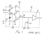
- This output circuit has been demonstrated by M.H. White et al in a publication of "IEEE JOURNAL OF SOLID-STATE CIRCUITS" Vol. SC-9 (February, 1974), pp 1-12 and is shown in Fig. 1 of the attached drawings in a simplified fashion.
- the output circuit shown in Fig. 1 includes an output-detection circuit 20 and a clamp circuit 30.
- the output-detection circuit 20 is formed on a silicon substrate together with a charge transfer region 10 in which a channel is formed for transferring charges. Charges transferred through the channel are injected into a diode 27 which is formed as a floating diffusion region in the charge transfer region 10 in contact with the channel.
- a change in potential at an electrode P of the diode 27 is detected and amplified by a source follower circuit formed of transistors 22 and 23. Thereafter, the detected and amplified potential change is applied to the clamp circuit 30 having a capacitor 36, a transistor 35 and a buffer amplifier 4, thus obtaining an output the DC level of which is clamped at V CL by the clamp circuit 30.
- a transistor 21 is a depletion type MOS transistor which functions as a reset transistor of the diode 27 and the reference symbols RD and ⁇ R denote a reset drain terminal held at a constant potential and reset pulse for operating the reset transistor 27, respectively. Further, AG denotes a bias voltage for controlling a DC current flowing through the source follower circuit.
- the threshold voltages V T2 and V T3 of the MOS transistors 22 and 23 vary due to variations in the manufacturing process and, therefore, it has heretofore been impossible to adjust the level of the output DC potential V OUT as will be understood from the formula (2). Accordingly, it has heretofore been difficult to connect directly the charge transfer device with a peripheral circuit using the output V OUT . Therefore, it is necessary to interpose the clamp circuit 30 or the like as shown in Fig. 3 in order to control the DC level together with to remove the affection from the pulses for operating the charge transfer region 10.
- an output circuit of a charge transfer device comprising an output-detection circuit receiving charges to inject them into a floating diffusion region for converting the quantity of the charges into a voltage form output signal, the floating diffusion region being reset periodically to a constant voltage, an output holding section holding a D.C. level of the voltage form output signal, a comparing section comparing the D.C. level held by the output holding section with a reference D.C. voltage, and a means for controlling the constant voltage so as to control the D.C. level of the voltage form output signal to the reference D.C. voltage.
- the control of the D.C. level of the voltage form output signal may be achieved by constituting the output holding section with the same constitution as the output-detection circuit and controlling the constant voltages applied to the output-detection circuit and the output holding circuit by the comparison result of the comparing section.
- the control of the D.C. level of the voltage form output signal may be alternatively achieved by constituting the output holding section with a sample hold circuit holding the voltage form output signal at a time when the floating diffusion region is reset to the constant voltage, and controlling the constant voltage by the comparison result of the comparing section.
- the constant voltage to which the floating diffusion region is reset is controlled by the output holding section, the comparing section and the controlling means, so as to keep the D.C. level of the voltage form output signal at the reference D.C. voltage, it is possible to give a constant and controlled D.C. level to the voltage form output signal even if the threshold voltages of the transistors used vary. Due to this constant and controlled D.C. level, the voltage form output signal can be directly applied to a circuit using the CCD output without interposing any clamp circuit. There is another merit based on the constant and controlled D.C. level that the derived voltage form output signal does not have a noise component which fluctuates the D.C. level of the voltage form output signal by the affection of the pulses for operating the charge transfer device.
- Fig. 2 is a circuit diagram showing a first embodiment of the present invention.
- a charge transfer device is formed on a silicon substrate with a charge transfer region 70 and an output detection circuit 60.
- the charge transfer region 70 has a channel region on which a plurality of transfer electrodes are formed in series via a thin-insulator film to form a charge coupled device.
- a diode 67 is formed as a floating diffused region of a conductivity type opposite to the silicon substrate to receive charges transferred through the channel region.
- the floating diffused region is connected to receive a reset voltage R DB through a reset transistor 61.
- the ON and OFF of the reset transistor 61 is controlled by a reset pulse ⁇ R applied to a gate electrode of the reset transistor 61.
- a reset pulse ⁇ R applied to a gate electrode of the reset transistor 61.
- a bias-current control transistor 63 is connected to the source electrode of the source-follower transistor 62 as a load.
- the bias current flowing through the source-follower transistor 62 is controlled by a bias control voltage V AG at a terminal AG.
- An output signal Vout B is derived from the source electrode of the source-follower transistor 62.
- a dummy output circuit 50 is employed to hold the same DC level as the output signal V out B .
- the DC level held by the dummy output circuit 50 is derived as the output V out A .
- a diode 57 and transistors 51 to 53 having the same dimensions and impurity concentrations as the diode 67 and the transistors 61 to 63 are connected in the same circuit as the output-detection circuit 60, except for the connection of the gate electrode of the transistor 51, to produce the same DC voltage as the output signal V out B as the output V out A .
- the same reset voltage V RD the same bias-control voltage V AG and the same power voltage V DD are similarly applied to the terminals RDA, AG and OD in the dummy output circuit 50.
- the output V out A of the dummy output circuit 50 is compared with a reference voltage V ref . by a comparator 5.
- the comparison result is commonly applied to the terminals RDA and RDB as the reset voltage V RD .
- the dummy output circuit 50 and the comparator 5 forms a feedback loop to control the level of the output V out A to have a value of the reference voltage V ref .
- the comparison result of the comparator 5 that is, the reset voltage V RD to the terminal RDB
- the DC level of the output V out B from the output-detection circuit 60 is controlled to have the value of the reference voltage V ref .
- the output V out A of the dummy output circuit 50 is compared with a reference voltage Vref by a comparator 5. Assuming that V out A > V ref , the output voltage of the comparator 5 lowers to lower the reset voltage V RD . When the reset voltage V RD lowers, since the transistor 51 is constantly ON, the gate potential of the source-follower transistor 52 also lowers, resulting in a lowering in the output V out A . The lowering of the output V out A stops when the output V out A becomes equal to the reference voltage Vref. In this way, the DC voltage level of the output V out A is constantly controlled so as to be the same as the reference voltage Vref.
- the dummy output circuit 50 is constructed of the diode 57 and the transistors 51 to 53 having the same dimensions and the same impurity concentrations as those of the diode 67 and the transistors 61 to 63 of the output detection circuit 60 to have the same stray capacitance and the same voltage gains, respectively.
- the dummy output circuit 50 thus formed of the same constituent elements as those of the output-detection circuit 60 has the same input-output characteristics as those of the latter.
- the diode 67 in the output-detection circuit 60 is constituted of a floating diffusion region formed at an end of a channel portion in the charge transfer region 70 and the potential at the node between the diode 67 and the reset transistor 61 is outputted through the source follower circuit formed of the transistors 62 and 63 to be directly applied to a peripheral circuit using the output of the charge transfer region 70 or a CCD device.
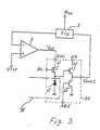
- Fig. 3 is a circuit diagram showing a second preferred embodiment of the present invention.
- This embodiment differs from the first preferred embodiment shown in Fig. 2 in that a sample-hold circuit (S/H) 2 is employed in place of the dummy output circuit 50 for holding the DC level of the output-detection circuit 40.
- the sampled voltage and the reference voltage V ref are compared with each other by the comparator 5 to control the reset voltage V RD at the terminal RDC.
- the basic feedback operation of this embodiment is the same as that of the first embodiment shown in Fig. 2.
- the DC level of the output V out C from the output-detection circuit 60 is held at the reference voltage V ref .
- the S/H pulse ⁇ SH is synchronized with the reset pulse ⁇ R so that, at least during the period when the reset pulse ⁇ R is ON, the DC level of the output V out C is sampled to be held, whereas, during the period when a signal involving the charge information is being outputted (i.e., during the period when the reset pulse ⁇ R is OFF), the DC level of the output V out C is not sampled.
- the arrangement is such that the sample-and-hold operation is conducted only during the period when the DC level of the output V out C is being outputted.
- the sampled DC level is compared with the reference voltage V ref to apply the comparison result to the terminal RDC (drain electrode of the reset transistor 61) as the reset voltage V RD . Due to the feedback operation in a loop of the output-detection circuit 60, the sample-hold circuit 2 and the comparator 5, the DC level of the output V out C is controlled to keep the same level as the reference voltage Vref, similarly to the first preferred embodiment shown in Fig. 2.
- sample-hold circuit 2 any kind of the well-known sample-hold circuit may be used.
- One example is shown in the above-mentioned publication "IEEE JOURNAL OF SOLID-STATE CIRCUITS" Vol. SC-9 (February 1974) page 4, at the right-hand side of Fig. 5 in which the switch 2 should be formed of a MOSFET.
- the output circuit of a charge transfer device incorporates a feedback circuit which applies a reset voltage having a controlled potential to a floating diffusion region through a reset transistor for resetting the charges in the floating diffusion region and is, therefore, capable of controlling the DC level of the output signal which varies in accordance with manufacturing error of circuit elements in the output circuit, so that it is advantageously possible to connect the output circuit directly to a peripheral circuit using the output signal.
- the above-described feedback circuit may be applied not only to a floating diffusion type sense amplifier but also to a floating gate type sense amplifier.
Landscapes
- Solid State Image Pick-Up Elements (AREA)
- Electronic Switches (AREA)
- Transforming Light Signals Into Electric Signals (AREA)
Applications Claiming Priority (2)
| Application Number | Priority Date | Filing Date | Title |
|---|---|---|---|
| JP63005231A JPH084137B2 (ja) | 1988-01-12 | 1988-01-12 | 電荷転送装置の出力回路 |
| JP5231/88 | 1988-01-12 |
Publications (3)
| Publication Number | Publication Date |
|---|---|
| EP0324456A2 true EP0324456A2 (fr) | 1989-07-19 |
| EP0324456A3 EP0324456A3 (en) | 1990-10-31 |
| EP0324456B1 EP0324456B1 (fr) | 1995-05-17 |
Family
ID=11605412
Family Applications (1)
| Application Number | Title | Priority Date | Filing Date |
|---|---|---|---|
| EP89100428A Expired - Lifetime EP0324456B1 (fr) | 1988-01-12 | 1989-01-11 | Circuit de sortie d'un dispositif de transfert de charge |
Country Status (4)
| Country | Link |
|---|---|
| US (1) | US4974239A (fr) |
| EP (1) | EP0324456B1 (fr) |
| JP (1) | JPH084137B2 (fr) |
| DE (1) | DE68922627T2 (fr) |
Cited By (2)
| Publication number | Priority date | Publication date | Assignee | Title |
|---|---|---|---|---|
| US7808535B2 (en) | 2000-04-12 | 2010-10-05 | Semiconductor Energy Laboratory Co., Ltd. | Semiconductor device and method of driving the same |
| WO2021203544A1 (fr) * | 2020-04-10 | 2021-10-14 | 深圳市华星光电半导体显示技术有限公司 | Circuit goa et panneau d'affichage |
Families Citing this family (14)
| Publication number | Priority date | Publication date | Assignee | Title |
|---|---|---|---|---|
| JP2707784B2 (ja) * | 1990-03-10 | 1998-02-04 | 日本電気株式会社 | 電荷転送装置 |
| JP2666522B2 (ja) * | 1990-05-14 | 1997-10-22 | 日本電気株式会社 | 電荷転送装置 |
| KR920006991A (ko) * | 1990-09-25 | 1992-04-28 | 김광호 | 반도체메모리 장치의 고전압발생회로 |
| JP2586727B2 (ja) * | 1990-11-09 | 1997-03-05 | 三菱電機株式会社 | 電荷検出回路の制御装置 |
| US5349303A (en) * | 1993-07-02 | 1994-09-20 | Cirque Corporation | Electrical charge transfer apparatus |
| FR2707440B1 (fr) * | 1993-07-09 | 1995-08-18 | Thomson Csf Semiconducteurs | Convertisseur charge-tension à rétroaction commandée. |
| JP4305970B2 (ja) * | 1998-06-05 | 2009-07-29 | ソニー株式会社 | 固体撮像素子の駆動方法 |
| JP4200545B2 (ja) * | 1998-06-08 | 2008-12-24 | ソニー株式会社 | 固体撮像素子およびその駆動方法、並びにカメラシステム |
| US6730863B1 (en) | 1999-06-22 | 2004-05-04 | Cirque Corporation | Touchpad having increased noise rejection, decreased moisture sensitivity, and improved tracking |
| US20100078483A1 (en) * | 2008-09-26 | 2010-04-01 | Rong Liu | Arrangement for and method of generating uniform distributed line pattern for imaging reader |
| US7834676B2 (en) * | 2009-01-21 | 2010-11-16 | Samsung Electronics Co., Ltd. | Method and apparatus for accounting for changes in transistor characteristics |
| JP2010068545A (ja) * | 2009-12-21 | 2010-03-25 | Semiconductor Energy Lab Co Ltd | 半導体装置の駆動方法 |
| JP2012054952A (ja) * | 2011-09-28 | 2012-03-15 | Semiconductor Energy Lab Co Ltd | 半導体装置及び半導体装置の駆動方法 |
| JP5619122B2 (ja) * | 2012-12-19 | 2014-11-05 | 株式会社半導体エネルギー研究所 | 半導体装置、x線カメラ及び電子機器 |
Family Cites Families (8)
| Publication number | Priority date | Publication date | Assignee | Title |
|---|---|---|---|---|
| US3946368A (en) * | 1974-12-27 | 1976-03-23 | Intel Corporation | System for compensating voltage for a CCD sensing circuit |
| US4156818A (en) * | 1975-12-23 | 1979-05-29 | International Business Machines Corporation | Operating circuitry for semiconductor charge coupled devices |
| US4099075A (en) * | 1977-03-23 | 1978-07-04 | General Electric Company | Signal detection apparatus using an adaptive threshold |
| JPS58177596A (ja) * | 1982-04-13 | 1983-10-18 | Sony Corp | 固体デジタルメモリの信号出力回路 |
| JPS5919297A (ja) * | 1982-07-23 | 1984-01-31 | Toshiba Corp | 電荷結合装置の出力回路 |
| US4556851A (en) * | 1983-08-22 | 1985-12-03 | Rca Corporation | Reduction of noise in signal from charge transfer devices |
| JPS6358968A (ja) * | 1986-08-29 | 1988-03-14 | Mitsubishi Electric Corp | 電荷結合素子 |
| JP2635325B2 (ja) * | 1987-04-17 | 1997-07-30 | キヤノン株式会社 | 固体撮像装置 |
-
1988
- 1988-01-12 JP JP63005231A patent/JPH084137B2/ja not_active Expired - Lifetime
-
1989
- 1989-01-11 EP EP89100428A patent/EP0324456B1/fr not_active Expired - Lifetime
- 1989-01-11 DE DE68922627T patent/DE68922627T2/de not_active Expired - Fee Related
- 1989-01-12 US US07/296,574 patent/US4974239A/en not_active Expired - Lifetime
Cited By (9)
| Publication number | Priority date | Publication date | Assignee | Title |
|---|---|---|---|---|
| US7808535B2 (en) | 2000-04-12 | 2010-10-05 | Semiconductor Energy Laboratory Co., Ltd. | Semiconductor device and method of driving the same |
| US8203636B2 (en) | 2000-04-12 | 2012-06-19 | Semiconductor Energy Laboratory Co., Ltd. | Semiconductor device and method of driving the same |
| US8355065B2 (en) | 2000-04-12 | 2013-01-15 | Semiconductor Energy Laboratory Co., Ltd. | Semiconductor device and method of driving the same |
| US8743250B2 (en) | 2000-04-12 | 2014-06-03 | Semiconductor Energy Laboratory Co., Ltd. | Semiconductor device and method of driving the same |
| US9019408B2 (en) | 2000-04-12 | 2015-04-28 | Semiconductor Energy Laboratory Co., Ltd. | Semiconductor device and method of driving the same |
| US9274236B2 (en) | 2000-04-12 | 2016-03-01 | Semiconductor Energy Laboratory Co., Ltd. | Semiconductor device and method of driving the same |
| US9568615B2 (en) | 2000-04-12 | 2017-02-14 | Semiconductor Energy Laboratory Co., Ltd. | Semiconductor device and method of driving the same |
| WO2021203544A1 (fr) * | 2020-04-10 | 2021-10-14 | 深圳市华星光电半导体显示技术有限公司 | Circuit goa et panneau d'affichage |
| US11705034B2 (en) | 2020-04-10 | 2023-07-18 | Shenzhen China Star Optoelectronics Semiconductor Display Technology Co., Ltd. | GOA circuit and display panel |
Also Published As
| Publication number | Publication date |
|---|---|
| JPH01181564A (ja) | 1989-07-19 |
| EP0324456A3 (en) | 1990-10-31 |
| EP0324456B1 (fr) | 1995-05-17 |
| JPH084137B2 (ja) | 1996-01-17 |
| DE68922627D1 (de) | 1995-06-22 |
| US4974239A (en) | 1990-11-27 |
| DE68922627T2 (de) | 1995-12-21 |
Similar Documents
| Publication | Publication Date | Title |
|---|---|---|
| EP0324456B1 (fr) | Circuit de sortie d'un dispositif de transfert de charge | |
| US4463383A (en) | Image pickup apparatus | |
| KR0175299B1 (ko) | Fet 비교기 회로 | |
| EP0875904A2 (fr) | Circuit échantillonneur-bloqueur | |
| EP0407859B1 (fr) | Comparateur à haute vitesse se plaçant automatiquement au point zéro | |
| US4528684A (en) | Charge-coupled device output circuit | |
| US6600513B1 (en) | Charge transfer device | |
| US4984256A (en) | Charge transfer device with booster circuit | |
| US4633101A (en) | Semiconductor sample and hold switching circuit | |
| KR910007841B1 (ko) | 전하전송소자 | |
| US5276723A (en) | Floating diffusion type charge detection circuit for use in charge transfer device | |
| US4700085A (en) | Circuit for detecting signal charges transferred in a charge transfer device | |
| US4050065A (en) | Dual slope analog to digital converter with delay compensation | |
| JP2777302B2 (ja) | オフセット検出回路、出力回路および半導体集積回路 | |
| US5029189A (en) | Input structure for charge coupled devices with controllable input bias | |
| US5252868A (en) | CMOS amplifier circuit and CCD delay line with CMOS amplifier | |
| EP0349981A2 (fr) | Circuit logique | |
| US4978925A (en) | Unity-gain CMOS/SOS zero-offset buffer | |
| EP0415852B1 (fr) | Circuit d'entrée pour ligne à retard CCD | |
| JP3701037B2 (ja) | サンプル・ホールド回路 | |
| JP2000152090A (ja) | 固体撮像装置 | |
| CA1234917A (fr) | Structure d'entree pour dispositifs a transfert de charge a polarisation d'entree controlable | |
| JP2707784B2 (ja) | 電荷転送装置 | |
| US5115155A (en) | CCD delay line | |
| EP0522292B1 (fr) | Dispositif détecteur de charge |
Legal Events
| Date | Code | Title | Description |
|---|---|---|---|
| PUAI | Public reference made under article 153(3) epc to a published international application that has entered the european phase |
Free format text: ORIGINAL CODE: 0009012 |
|
| 17P | Request for examination filed |
Effective date: 19890111 |
|
| AK | Designated contracting states |
Kind code of ref document: A2 Designated state(s): DE FR GB |
|
| PUAL | Search report despatched |
Free format text: ORIGINAL CODE: 0009013 |
|
| AK | Designated contracting states |
Kind code of ref document: A3 Designated state(s): DE FR GB |
|
| ITF | It: translation for a ep patent filed | ||
| 17Q | First examination report despatched |
Effective date: 19921120 |
|
| GRAA | (expected) grant |
Free format text: ORIGINAL CODE: 0009210 |
|
| AK | Designated contracting states |
Kind code of ref document: B1 Designated state(s): DE FR GB |
|
| REF | Corresponds to: |
Ref document number: 68922627 Country of ref document: DE Date of ref document: 19950622 |
|
| ET | Fr: translation filed | ||
| PLBE | No opposition filed within time limit |
Free format text: ORIGINAL CODE: 0009261 |
|
| STAA | Information on the status of an ep patent application or granted ep patent |
Free format text: STATUS: NO OPPOSITION FILED WITHIN TIME LIMIT |
|
| 26N | No opposition filed | ||
| REG | Reference to a national code |
Ref country code: GB Ref legal event code: IF02 |
|
| PGFP | Annual fee paid to national office [announced via postgrant information from national office to epo] |
Ref country code: GB Payment date: 20020109 Year of fee payment: 14 |
|
| PGFP | Annual fee paid to national office [announced via postgrant information from national office to epo] |
Ref country code: FR Payment date: 20020110 Year of fee payment: 14 |
|
| PGFP | Annual fee paid to national office [announced via postgrant information from national office to epo] |
Ref country code: DE Payment date: 20020212 Year of fee payment: 14 |
|
| PG25 | Lapsed in a contracting state [announced via postgrant information from national office to epo] |
Ref country code: GB Free format text: LAPSE BECAUSE OF NON-PAYMENT OF DUE FEES Effective date: 20030111 |
|
| PG25 | Lapsed in a contracting state [announced via postgrant information from national office to epo] |
Ref country code: DE Free format text: LAPSE BECAUSE OF NON-PAYMENT OF DUE FEES Effective date: 20030801 |
|
| GBPC | Gb: european patent ceased through non-payment of renewal fee | ||
| PG25 | Lapsed in a contracting state [announced via postgrant information from national office to epo] |
Ref country code: FR Free format text: LAPSE BECAUSE OF NON-PAYMENT OF DUE FEES Effective date: 20030930 |
|
| REG | Reference to a national code |
Ref country code: FR Ref legal event code: ST |