EP0324629A2 - Vielfachstecker - Google Patents
Vielfachstecker Download PDFInfo
- Publication number
- EP0324629A2 EP0324629A2 EP89300286A EP89300286A EP0324629A2 EP 0324629 A2 EP0324629 A2 EP 0324629A2 EP 89300286 A EP89300286 A EP 89300286A EP 89300286 A EP89300286 A EP 89300286A EP 0324629 A2 EP0324629 A2 EP 0324629A2
- Authority
- EP
- European Patent Office
- Prior art keywords
- connector
- module
- housing
- sets
- contact pins
- Prior art date
- Legal status (The legal status is an assumption and is not a legal conclusion. Google has not performed a legal analysis and makes no representation as to the accuracy of the status listed.)
- Withdrawn
Links
Images

Classifications
-
- H—ELECTRICITY
- H01—ELECTRIC ELEMENTS
- H01R—ELECTRICALLY-CONDUCTIVE CONNECTIONS; STRUCTURAL ASSOCIATIONS OF A PLURALITY OF MUTUALLY-INSULATED ELECTRICAL CONNECTING ELEMENTS; COUPLING DEVICES; CURRENT COLLECTORS
- H01R13/00—Details of coupling devices of the kinds covered by groups H01R12/70 or H01R24/00 - H01R33/00
- H01R13/66—Structural association with built-in electrical component
- H01R13/665—Structural association with built-in electrical component with built-in electronic circuit
- H01R13/6666—Structural association with built-in electrical component with built-in electronic circuit with built-in overvoltage protection
Definitions
- This invention relates to a multicontact connector for making connections between first and second sets of conductors.
- Multicontact connectors are widely used to make connections between first and second sets of conductors, which may be the conductors of a wire bundle or of a multiconductor cable which may be, for example a flat or a round cable.
- the conductors of one or both sets may be contacts on a piece of equipment, which may be formed as, for example, a plug or a socket to engage a cooperating socket or plug respectively which is connected to another set of conductors.
- US-4295704 discloses a multicontact connector for terminating a multiconductor cable.
- the connector body houses electrical contacts, and has a passage formed in its wall which allows the contacts to be probed from outside the body.
- US-4487464 discloses a multicontact connector for connecting a multiconductor cable to contacts on a printed wiring board.
- the connector housing has an array of electrical contacts arranged within a cavity within it, and has a slot in its wall for receiving a strip of conductive material which can be used to interconnect predetermined ones of the pins.
- US-4473755 discloses a device for protecting audio equipment from noise generated by digital electronic apparatus.
- the device commprises a connector which includes a metal casing and a plurality of connector pins, and a plurality capacitors, each capacitor being connected between a respective connector pin and the metal casing.
- the present invention provides a connector which comprises a multicontact connector for making connections between first and second sets of conductors, comprising:
- the connector of the invention has the advantage that it can readily be adapted to suit the requirements of a par ticular application by selection of a module which houses appropriate electronic components.
- the selected module can conveniently be fitted to the housing by virtue of the shell causing the module and the housing to fit together.
- the ease with which the module can be fitted to, and removed from, the connector facilitates repair, testing or replacement of the components. This also allows the inventory of connectors to be kept small. Furthermore, when it is necessary to replace an electronic component because it is faulty, the cost of doing so is very much reduced by replacing a module which houses the faulty component compared with replacing the entire connector as would be necessary if the component were an integral part of the entire connector.
- the conductors to which the contacts are to be connected may be, for example, the conductors of a cable, or contacts on a piece of equipment.
- the connector is one part of a plug and socket combination, one of the sets of conductors will generally be provided by the contacts in the other part of the combination.
- the module When the connector is a round connector, the module will preferably be arc-shaped, the angle of the arc occupied by the module preferably being less than about 90°.
- the connector is a flat connector which is suitable for forming connections to flat cable.
- a module can be provided as a planar element which can be fitted on a principal surface of the connector.
- the connector may be of the type which comprises a shell and one or more housings in the form of wafers within the shell, the wafers housing contact pins for connection to first and second sets of conductors.
- the connector when there is one wafer, it will preferably receive a module on one or both of its principal surfaces.
- each wafer receive a module on its exposed principal surface.
- the nature and arrangement of the electronic components in the module will be selected according to the function that they are required to perform. For example, they may be arranged to filter a signal that is to be transmitted between the first and second sets of conductors through a connector. They may be arranged to protect sensitive equipment that is connected, directly or indirectly, to the connector from a potentially damaging electrical event such as high current or voltage, which may be, for example, in the form of a pulse. Such a damaging event may result from a lightning strike on the conductors. The equipment may be protected for example against a signal whose voltage exceeds a predetermined value, whose current exceeds a predetermined value, or whose frequency is outside a predetermined range.
- Protection may be influenced by for example the conditions in which the components are operating or by the signal itself.
- sensitive equipment may be protected by use of a material whose resistivity is dependent on temperature, such as a conductive polymer material which has a positive temperature coefficient of resistivity.
- a suitable material is disclosed in US-4329726, and devices for circuit protection which comprise such a material are disclosed in US-4237441 and US-4238812. The matter disclosed in the listed documents is incorporated herein by these references.
- Use of a material whose resistivity varies with temperature in this way ensures protection in the event of an external temperature rise or, particularly usefully, in the event of a potentially damaging high current being transmitted in the conductors.
- Protection of sensitive equipment may also be made dependent on the signal itself, by being sensitive to a voltage surge. Such protection can be achieved by use of a material or a device as disclosed in any of EP-A-196891, EP-A-198624, EP-A-242902, EP-A-259176, EP-A-259177, EP-A-259178, EP-A-259179, EP-A-261939, EP-A-261937 and EP-A-261938.
- the electronic components include a threshold switch having an energy to latch (i.e., the electrical energy required to force the switch into its low resistance state) of at least 40 mJ measured on a sample of 10 micrometer thickness and 1 mm2 area using electrical energy of 1 MHz frequency, and in addition or alternatively a current carrying capacity of at least about 20 amps, especially at least about 40 amps.
- the voltage at which the switch is caused to latch is preferably from about 50V to about 500V, especially from 90V to about 150V.
- a threshold switch a composition which comprises:
- threshold switches are connected to each of the contact pins, between the contact pins and a conductor at a reference potential, and a capacitor is connected in series with each switching element. Further information on this arrangement can be found in EP-A-259178, referred to above.
- the module is provided as a package in which the electronic components are sealed.
- the module may comprise electronic components with appropriate connectors and sealed within potting material such as an epoxy resin.
- At least one electrical component is connected between at least one of the contact pins and a conductor which, when the connector is in use, is at a reference potential.
- the said conductor may for example be at ground potential.
- the conductor at the reference potential may be one of the conductors which is connected to a contact on the connector.
- the component When the housing is constructed at least partially of a conductive material, the component may be connected between one of the contact pins and the housing, the housing being at the reference potential.
- the contact pins may be arranged in first and second sets for connection respectively to first and second sets of conductors, the connection between respective pins of the first and second sets being made through electronic components in the module.
- the signal transmitted through the connector can be modified individually for each contact pin, and the signal passes through one or more electronic components on passing through the connector.
- This arrangement may be used to protect sensitive electrical equipment by arranging the electronic components to filter the signal passing between each pair of contact pine of the first and second sets. For example the equipment may be protected against a signal of a potentially damaging frequency by arranging the components to filter out frequencies outside a predetermined range.
- connection between the contacts and the module may be made by means of pins which fit into cooperating recesses in the manner of a plug and socket.
- a spur pin is attached at one end to each contact pin and is received at its other end in a recess in the module.
- the spur pin and the contact pin may be formed as one unit, or they may be formed separately and then joined together, for example by welding or by means of a solder.
- each contact pin and spur pin assembly will preferably be approximately L-shaped; the spur pin portions between which the module makes the connections will be provided by one of the arms of the L's, and the conductors will be made through the other arms of the L's.
- the contact pin and spur pin assembly will preferably be approximately T-shaped; the spur pin portion will be provided by the upright arm of the T, and the connections to the conductors of the first and second sets will be made through the horizontal arms of the T.
- the module and the housing are provided with a latch so that the module is retained securely on the housing when the housing is in use, when it can be subjected to severe vibration and shock.
- the module may be retained on the housing by a C-shaped spring or by a screw threaded clamp.
- the or each module may be forced against its corresponding housing by the walls of the shell when the module and housing are inserted in the shell.
- an internal dimension of the shell may decrease gradually as the housing and module are inserted into the shell so that the housing and module, contacting opposite surfaces of the shell, are forced towards one another.
- the connector includes means for sealing the electrical connections between the housing and the module.
- a preferred form of seal takes the form of a gasket of a sealing material such as a gel or of an elastomeric material such as silicone rubber.
- the gasket may be positioned between the mating surfaces of the module and the housing, and the seal may be enhanced by forcing the module and the housing towards one another, for example as described above.
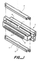
- Figure 1 shows a connector which comprises a housing 1 and a plurality of contact pins 3 in two layers for connection at one end 5 to a plurality of conductors of a wire bundle, for example by wire wrapping, and for connection at their other end 7 to a cooperating connector (not shown).
- Each contact pin has a spur pin 9 attached to it, which extends from the contact pin and protrudes above a surface of the connector.
- a module 11 is fitted on each surface of the connector such that the spur pins 9 are received in recesses 13 therein.
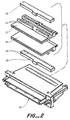
- Figure 2 shows a connector which comprises a plug shell 20 and a pair of wafers 21.
- the wafers house contact pins for connection to first and second sets of conductors.
- Spur pins 23 protrude above the surface of the wafer to engage recesses 24 in a module 25 which houses electronic components.
- the conductors of a flat cable are connected to the contact pins of one of the wafers 21, the module 25 is located on the spur pins 23, and the wafer is inserted into the plug shell 20 for connection to an appropriate socket, which may be connected to a piece of electrical equipment or to another cable.
- Figure 3 shows a connector which comprises a housing 31 having a contact pin 33 extending through it.
- One end 35 of the pin extends beyond the housing for connection to a conductor of a multiconductor cable, for example by means of a solder.
- the other end 37 of the pin is recessed within the housing, for mating with a corresponding pin on a cooperating socket.
- a spur pin 39 is attached at one end to the contact pin 33 and protrudes at its other end above the surface of the housing, for connection to a module 41.
- the spur pin and contact pin assembly is thus T-shaped. It is preferably formed as one unit.
- Figure 4 shows a connector which comprises a housing 51 having two L-shaped contact pins 53,55.
- One of the contact pins 53 extends beyond the housing for connection to a conductor of a multiconductor cable.
- the end of the other contact pin 55 is recessed within the housing, for mating with a corresponding pin on a cooperating socket.
- Spur pins 57 are attached to each of the contact pins and protrude above the surface of the housing.
- the spur pins 57 are received within recesses in a module 59 which houses electronic components, by means of which the spur pins, and therefore also the contact pins, are interconnected.
- Figure 5 shows a connector of the type shown in Figure 2 which comprises a connector shell 61 and a pair of wafers 63, each of which houses contact pins 65 and spur pins 67.
- a module 69 is located on the exposed principal surface of each of the wafers 63 where they are electrically connected to the spur pins 67.
- a layer of silicone rubber 71 is located between the opposing surfaces of the modules and the wafers for sealing the electrical connections between them.
- the modules and the wafers are forced towards one another, so as to compress the layers of silicone rubber and therefore to enhance the seal between the modules and the wafers, on insertion into the connector shell 61. This is caused by the gradual decrease in the internal dimension of the shell, from right to left as depicted in Figure 5 due to the increase in thickness of the wall of the plug shell.
Landscapes
- Engineering & Computer Science (AREA)
- Microelectronics & Electronic Packaging (AREA)
- Details Of Connecting Devices For Male And Female Coupling (AREA)
- Coupling Device And Connection With Printed Circuit (AREA)
Applications Claiming Priority (2)
| Application Number | Priority Date | Filing Date | Title |
|---|---|---|---|
| US07/143,796 US4820203A (en) | 1988-01-14 | 1988-01-14 | Multicontact connector |
| US143796 | 1988-01-14 |
Publications (2)
| Publication Number | Publication Date |
|---|---|
| EP0324629A2 true EP0324629A2 (de) | 1989-07-19 |
| EP0324629A3 EP0324629A3 (de) | 1990-04-25 |
Family
ID=22505683
Family Applications (1)
| Application Number | Title | Priority Date | Filing Date |
|---|---|---|---|
| EP89300286A Withdrawn EP0324629A3 (de) | 1988-01-14 | 1989-01-12 | Vielfachstecker |
Country Status (6)
| Country | Link |
|---|---|
| US (1) | US4820203A (de) |
| EP (1) | EP0324629A3 (de) |
| JP (1) | JPH01231279A (de) |
| BR (1) | BR8900107A (de) |
| CA (1) | CA1296787C (de) |
| IL (1) | IL88952A0 (de) |
Cited By (1)
| Publication number | Priority date | Publication date | Assignee | Title |
|---|---|---|---|---|
| DE9104337U1 (de) * | 1991-04-10 | 1992-08-06 | Hermann Kleinhuis GmbH & Co KG, 5880 Lüdenscheid | Überspannungsschutzadapter |
Families Citing this family (3)
| Publication number | Priority date | Publication date | Assignee | Title |
|---|---|---|---|---|
| WO1995013621A1 (en) * | 1993-11-12 | 1995-05-18 | Alcoa Fujikura Ltd. | Short circuit protected splice connector |
| TW417872U (en) * | 1999-05-15 | 2001-01-01 | Hon Hai Prec Ind Co Ltd | Electrical connector |
| US7207843B1 (en) * | 2006-04-24 | 2007-04-24 | Hung-Lin Chang | Spark leakage shutoff protective device for plug |
Family Cites Families (15)
| Publication number | Priority date | Publication date | Assignee | Title |
|---|---|---|---|---|
| US3343034A (en) * | 1961-06-21 | 1967-09-19 | Energy Conversion Devices Inc | Transient suppressor |
| US3271591A (en) * | 1963-09-20 | 1966-09-06 | Energy Conversion Devices Inc | Symmetrical current controlling device |
| US3993394A (en) * | 1974-07-31 | 1976-11-23 | Raychem Corporation | Connector half having connector wafer retained therein |
| US4274699A (en) * | 1978-04-27 | 1981-06-23 | E. I. Du Pont De Nemours And Company | Press fit terminal with spring arm contact for edgecard connector |
| US4206962A (en) * | 1978-06-05 | 1980-06-10 | Amp Incorporated | Data/logic connector |
| US4295704A (en) * | 1979-12-03 | 1981-10-20 | Thomas & Betts Corporation | Side probeable connector using flat cable |
| JPS57168540A (en) * | 1981-04-10 | 1982-10-16 | Nissan Motor Co Ltd | Noise preventing device and its production for electronic controller |
| US4487464A (en) * | 1982-09-07 | 1984-12-11 | At&T Bell Laboratories | Electrical socket connector construction |
| US4575704A (en) * | 1984-01-27 | 1986-03-11 | Fire Savr | Electrical adaptor |
| WO1986002496A1 (en) * | 1984-10-16 | 1986-04-24 | Amp Incorporated | Electronic key assemblies |
| AU584998B2 (en) * | 1985-03-29 | 1989-06-08 | Raychem Limited | Circuit protection device |
| US4647717A (en) * | 1985-05-02 | 1987-03-03 | Raychem Corp. | Gel filled container |
| US4726776A (en) * | 1986-06-10 | 1988-02-23 | Amp Incorporated | Socket for zig-zag inline package |
| US4679885A (en) * | 1986-08-01 | 1987-07-14 | General Motors Corporation | Electrical component packaging assembly |
| US4772225A (en) * | 1987-11-19 | 1988-09-20 | Amp Inc | Electrical terminal having means for mounting electrical circuit components in series thereon and connector for same |
-
1988
- 1988-01-14 US US07/143,796 patent/US4820203A/en not_active Expired - Fee Related
-
1989
- 1989-01-11 BR BR898900107A patent/BR8900107A/pt unknown
- 1989-01-12 EP EP89300286A patent/EP0324629A3/de not_active Withdrawn
- 1989-01-13 IL IL88952A patent/IL88952A0/xx unknown
- 1989-01-13 JP JP1007519A patent/JPH01231279A/ja active Pending
- 1989-01-13 CA CA000588243A patent/CA1296787C/en not_active Expired - Fee Related
Cited By (1)
| Publication number | Priority date | Publication date | Assignee | Title |
|---|---|---|---|---|
| DE9104337U1 (de) * | 1991-04-10 | 1992-08-06 | Hermann Kleinhuis GmbH & Co KG, 5880 Lüdenscheid | Überspannungsschutzadapter |
Also Published As
| Publication number | Publication date |
|---|---|
| US4820203A (en) | 1989-04-11 |
| EP0324629A3 (de) | 1990-04-25 |
| IL88952A0 (en) | 1989-08-15 |
| BR8900107A (pt) | 1989-09-05 |
| CA1296787C (en) | 1992-03-03 |
| JPH01231279A (ja) | 1989-09-14 |
Similar Documents
| Publication | Publication Date | Title |
|---|---|---|
| RU2394322C1 (ru) | Многополюсный разрядник молниезащиты и/или защиты от перенапряжений, выполненный в виде клеммной колодки | |
| EP0801815B1 (de) | Aufhängungssystem für elektrische schaltung | |
| EP0635907B1 (de) | Gefilterter elektrischer Verbinder | |
| US6450837B1 (en) | Electrical connector having surge suppressing device | |
| US7497737B2 (en) | Subminiature electrical connector including over-voltage and over-current circuit protection | |
| US4804332A (en) | Filtered electrical device and method for making same | |
| US8908346B2 (en) | Overvoltage protection device | |
| EP0305186A2 (de) | Abgeschirmte elektrische Verbinder | |
| US5281150A (en) | Method and apparatus for connecting cable to the surface of printed circuit boards or the like | |
| WO1988005218A1 (en) | Filtered electrical device and method for making same | |
| CN1007482B (zh) | 电信装置连接器触排 | |
| WO1998034296A2 (en) | Multifunction electronic connector | |
| EP0843908B1 (de) | Überspannungsschutzvorrichtung für fernmeldeleitungen | |
| US4820203A (en) | Multicontact connector | |
| EP0724312B1 (de) | Elektrischer Verbinder mit Mehrstellungsfilteradapter | |
| CN111684671B (zh) | 具有防浪涌功能的连接器和包括该连接器的电路板 | |
| US5399099A (en) | EMI protected tap connector | |
| US6935879B2 (en) | Connectors having circuit protection | |
| WO1998027625A1 (en) | Telephone adaptor | |
| US3961226A (en) | Multi-terminal arrestor holder and connector module | |
| WO1997022998A1 (en) | Electrostatic discharge protection device | |
| EP0286440A2 (de) | Verbinderanordnung | |
| US4920443A (en) | Electrical protection assemblies | |
| JPS5873297A (ja) | 通信ラインのタ−ミナル構造 | |
| GB2224402A (en) | Solid state station protector device |
Legal Events
| Date | Code | Title | Description |
|---|---|---|---|
| PUAI | Public reference made under article 153(3) epc to a published international application that has entered the european phase |
Free format text: ORIGINAL CODE: 0009012 |
|
| 17P | Request for examination filed |
Effective date: 19890119 |
|
| AK | Designated contracting states |
Kind code of ref document: A2 Designated state(s): AT BE CH DE ES FR GB IT LI NL SE |
|
| PUAL | Search report despatched |
Free format text: ORIGINAL CODE: 0009013 |
|
| AK | Designated contracting states |
Kind code of ref document: A3 Designated state(s): AT BE CH DE ES FR GB IT LI NL SE |
|
| 17Q | First examination report despatched |
Effective date: 19921223 |
|
| STAA | Information on the status of an ep patent application or granted ep patent |
Free format text: STATUS: THE APPLICATION IS DEEMED TO BE WITHDRAWN |
|
| 18D | Application deemed to be withdrawn |
Effective date: 19940210 |