EP0324827B1 - Installation d'impression pourvue de circuits perfectionnes de formatage de donnees - Google Patents
Installation d'impression pourvue de circuits perfectionnes de formatage de donnees Download PDFInfo
- Publication number
- EP0324827B1 EP0324827B1 EP88906387A EP88906387A EP0324827B1 EP 0324827 B1 EP0324827 B1 EP 0324827B1 EP 88906387 A EP88906387 A EP 88906387A EP 88906387 A EP88906387 A EP 88906387A EP 0324827 B1 EP0324827 B1 EP 0324827B1
- Authority
- EP
- European Patent Office
- Prior art keywords
- memory
- image signals
- data
- shift register
- line
- Prior art date
- Legal status (The legal status is an assumption and is not a legal conclusion. Google has not performed a legal analysis and makes no representation as to the accuracy of the status listed.)
- Expired
Links
Images


Classifications
-
- G—PHYSICS
- G06—COMPUTING OR CALCULATING; COUNTING
- G06K—GRAPHICAL DATA READING; PRESENTATION OF DATA; RECORD CARRIERS; HANDLING RECORD CARRIERS
- G06K15/00—Arrangements for producing a permanent visual presentation of the output data, e.g. computer output printers
- G06K15/02—Arrangements for producing a permanent visual presentation of the output data, e.g. computer output printers using printers
- G06K15/12—Arrangements for producing a permanent visual presentation of the output data, e.g. computer output printers using printers by photographic printing, e.g. by laser printers
- G06K15/1238—Arrangements for producing a permanent visual presentation of the output data, e.g. computer output printers using printers by photographic printing, e.g. by laser printers simultaneously exposing more than one point
- G06K15/1242—Arrangements for producing a permanent visual presentation of the output data, e.g. computer output printers using printers by photographic printing, e.g. by laser printers simultaneously exposing more than one point on one main scanning line
- G06K15/1247—Arrangements for producing a permanent visual presentation of the output data, e.g. computer output printers using printers by photographic printing, e.g. by laser printers simultaneously exposing more than one point on one main scanning line using an array of light sources, e.g. a linear array
-
- G—PHYSICS
- G11—INFORMATION STORAGE
- G11C—STATIC STORES
- G11C7/00—Arrangements for writing information into, or reading information out from, a digital store
- G11C7/10—Input/output [I/O] data interface arrangements, e.g. I/O data control circuits, I/O data buffers
- G11C7/1015—Read-write modes for single port memories, i.e. having either a random port or a serial port
- G11C7/1018—Serial bit line access mode, e.g. using bit line address shift registers, bit line address counters, bit line burst counters
-
- H—ELECTRICITY
- H04—ELECTRIC COMMUNICATION TECHNIQUE
- H04N—PICTORIAL COMMUNICATION, e.g. TELEVISION
- H04N1/00—Scanning, transmission or reproduction of documents or the like, e.g. facsimile transmission; Details thereof
- H04N1/04—Scanning arrangements, i.e. arrangements for the displacement of active reading or reproducing elements relative to the original or reproducing medium, or vice versa
- H04N1/19—Scanning arrangements, i.e. arrangements for the displacement of active reading or reproducing elements relative to the original or reproducing medium, or vice versa using multi-element arrays
- H04N1/191—Scanning arrangements, i.e. arrangements for the displacement of active reading or reproducing elements relative to the original or reproducing medium, or vice versa using multi-element arrays the array comprising a one-dimensional [1D] array
- H04N1/192—Simultaneously or substantially simultaneously scanning picture elements on one main scanning line
- H04N1/193—Simultaneously or substantially simultaneously scanning picture elements on one main scanning line using electrically scanned linear arrays, e.g. linear CCD arrays
Definitions
- the present invention relates to non-impact printing apparatus for recording on a moving recording medium.
- printing apparatus which comprises a multiplicity of individually addressable and energizable point-like radiation sources, such as light-emitting diodes (LED's), arranged in a row(s) for exposing points upon a photoreceptor during movement thereof relative to and in a direction normal to the row(s).
- Driver circuits are provided for simultaneously energizing the radiation sources responsive to respective data bit input signals applied to the driver circuits during an information line period.
- the print or recording head includes a support upon which are mounted chips placed end to end and upon each of which are located a group of LED's.
- the driver circuits are incorporated in other chips located to the side of the linear array of LED chips.
- the driver circuits in this apparatus each include a shift register for serially receiving data-bit signals and for driving respective LED's in accordance with the data or image signals.
- the shift registers on adjacent chips are coupled together to function as a single "shift register assemblage" so that the data bits (image signals) flow down and fill the shift registers in the shift register assemblage bit by bit under clock control.
- the data management for this type of apparatus may be complex or simple depending upon the arrangement of the data.
- data management for distributing this data for use with a multiple array printhead may present some difficulties. This is due to the consecutive sequential order in which data is provided for a laser exposure device that employs, say, a rotating polygon to expose a line in the mainscanning direction, first pixel first, and so on until the last pixel on that line is exposed.
- consecutive sequential order refers to an order of data that is congruous with the order of the data as it is to appear on the recording medium.
- Data management is made particularly difficult where it is desired to provide a single buffer memory chip for storing a single line of data prior to feeding this data to the shift registers on the printhead.
- An image recording apparatus comprises a memory means that includes one or more, but less than a first predetermined plural number, N, of integrated circuit memory chips, having at least a second plural predetermined number, M, of memory sites for storing in said chip(s) as a buffer memory image signals representing a full line of image signals to be printed by said apparatus.
- Means are provided for writing serially the image signals to said memory means in consecutive sequential order.
- a recording means has said second predetermined number of recording elements and driver means for activating same for recording an image on a recording material on a line by line basis.
- a shift register assemblage means has the first predetermined number of shift register assemblages, each for storing image signals that are serially inputted into each shift register assemblage and for outputting said image signals in parallel to said driver means.
- the apparatus is characterized by intermediate register means for shifting image signals to each of said shift register assemblages; and extracting means for serially extracting image signals from said first memory means in consecutive sequential order and for feeding said image signals to said intermediate register means.
- the apparatus of the preferred embodiment will be described in accordance with an electrophotographic recording medium.
- the invention is not limited to apparatus for creating images on such a medium, as other media such as photographic film etc. may also be used within the spirit of the invention.
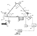
- an electrophotographic reproduction apparatus 10 includes a recording medium such as a photoconductive web 11 or other photosensitive medium that is trained about three transport rollers 12, 13 and 14, thereby forming an endless or continuous web.
- Roller 12 is coupled to a driver motor M in a conventional manner.
- Motor M is connected to a source of potential when a switch (not shown) is closed by a logic and control unit (LCU) 15.
- LCU logic and control unit
- the roller 12 is driven by the motor M and moves the web 11 in clockwise direction as indicated by arrow A. This movement causes successive image areas of web 11 to sequentially pass a series of electrophotographic work stations of the reproduction apparatus.
- a charging station 17 is provided at which the photoconductive surface 16 of the web 11 is sensitized by applying to such surface a uniform electrostatic primary charge of a predetermined voltage.
- the output of the charger may be controlled by a grid connected to a programmable power supply (not shown).
- the supply is in turn controlled by the LCU 15 to adjust the voltage level Vo applied onto the surface 16 by the charger 17.
- an electrostatic image is formed by modulating the primary charge on an image area of the surface 16 with selective energization of point-like radiation sources in accordance with signals provided by a data source 19 such as a computer.
- the point-like radiation sources are supported in a printhead 20 to be described in more detail below.
- a development station 21 includes developer which may consist of iron carrier particles and electroscopic toner particles with an electrostatic charge opposite to that of the latent electrostatic image. Developer is brushed over the photoconductive surface 16 of the web 11 and toner particles adhere to the latent electrostatic image to form a visible toner particle, transferable image.
- the development station may be of the magnetic brush type with one or two rollers. Alternatively, the toner particles may have a charge of the same polarity as that of the latent electrostatic image and develop the image in accordance with known reversal development techniques.
- the apparatus 10 also includes a transfer station 25 shown with a corona charger 22 at which the toner image on web 11 is transferred to a copy sheet S; and a cleaning station 28, at which the photoconductive surface 16 of the web 11 is cleaned of any residual toner particles remaining after the toner images have been transferred.
- a transfer station 25 shown with a corona charger 22 at which the toner image on web 11 is transferred to a copy sheet S
- a cleaning station 28 at which the photoconductive surface 16 of the web 11 is cleaned of any residual toner particles remaining after the toner images have been transferred.
- a copy sheet S is fed from a supply 23 to driver rollers 24, which then urge the sheet to move forward onto the web 11 in alignment with a toner image at the transfer station 25.
- the web has a plurality of indicia such as perforations along one of its edges. These perforations generally are spaced equidistantly along the edge of the web 11.
- suitable means 26 for sensing web perforations. This sensing produces input signals into the LCU 15 which has a digital computer, preferably a microprocessor.
- the microprocessor has a stored program responsive to the input signals for sequentially actuating, then de-actuating the work stations as well as for controlling the operation of many other machine functions. Additional or other encoding means may be provided as known in the art for providing the precise timing signals for control of the various functions of the apparatus 10.
- the printhead 20 is provided with a multiplicity of energizable point-like radiation sources 30, preferably light-emitting diodes (LED's) although other recording devices such as thermal devices, liquid crystal display elements or needle electrodes are also contemplated.
- Optical means 29 may be provided for focusing light from each of the LED's onto the photoconductive surface.
- the optical means preferably comprises an array of optical fibers such as sold under the name Selfoc, a trademark for a gradient index lens array sold by Nippon Sheet Glass, Limited. Due to the focusing power of the optical means 29, a row of emitters will be imaged on a respective transverse line on the recording medium.
- the printhead 20 comprises a suitable support with a series of LED chips 31 mounted thereon.
- Each of the chips 31 includes in this example 64 LED's arranged in a single row.
- Chips 31 are also arranged end-to-end in a row and where fifty-six LED chips are so arranged, the printhead will extend across the width of the web 11 and include 3584 LED's arranged in a single row.
- Each of these driver chips include circuitry for addressing the logic associated with each of 32 LED's to control whether or not an LED should be energized or activated. Two driver chips 40 are thus associated with each chip of 64 LED's.
- Each of the two driver chips will be coupled for driving of alternate LED's.
- one driver chip will drive the odd numbered LED's of the 64 LED's and the other will drive the even numbered LED's of these 64 LED's.
- the driver chips 40 are electrically connected in parallel to a plurality of lines 34-37 providing various electrical control signals and potentials.
- Lines 34 and 35 provide electrical energy for operating the various logic devices and current drivers in accordance with their voltage requirements.
- Lines 32 and 37 provide ground or return lines for lines 34 and 35, respectively.
- a series of lines, 36a, b and c provide clock signals and other pulses for controlling the movement of data to the LED's in accordance with known techniques.
- Data lines 33A, 33B, 33C and 33D are also provided for providing digital data or image signals in the form of either a high or low logic level.
- the driver chips each include a data-in and data-out port so that data is serially passed between appropriate chips.
- Driver chips having respective shift registers linked together as such comprise a "shift register assemblage.”
- the driver chips receiving the data for the odd numbered LED's are divided into two shift register assemblage groups.
- the first group of shift register assemblages receive data serially through line 33A.
- the second group of driver chips receive data through line 33B.
- the driver chips receiving the data for the even-numbered LED's are divided into two shift register assemblage groups and receive data over lines 33C, 33D, respectively.
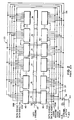
- each driver chip 40 includes a 32-bit bi-directional shift register 41.
- a logic signal carried over line R/LB determines the direction data will flow down this register. Assume that this chip is enabled to cause data to flow down the register from left to right as shown in FIG. 3.
- Data thus enters shift register 41 over line 33C through the driver chip's data-in port at the left from say the data-out port of a driver chip immediately to the left or from the LCU if the driver chip 40 is the first chip for data to enter. Data exits from this chip at the data-out port to be input to the next adjacent driver chip to the right of driver chip 40.
- Each latch register is associated with a particular LED and adjacent latch registers are associated with every other LED.
- a logic AND gate 43 is associated with each latch register and has one input coupled to the output of its respective latch register and its other input coupled to a line 36c for providing a strobe or timing pulse from the LCU. This strobe pulse determines when to trigger the LED's to turn on in relation to the position of the recording medium and the duration for which the LED's are turned on. All the AND gates have one of their inputs connected to this strobe line. The output of each of the AND gates is coupled to a logic circuit that is part of a constant current driver circuit 44.
- Leads to the constant current driver circuit include voltage supply and ground lines (35 and 37, respectively) to the logic devices therein as well as separate voltage and return lines (34 and 32, respectively) for providing current to the LED's.
- voltage supply and ground lines 35 and 37, respectively
- separate voltage and return lines 34 and 32, respectively
- several strobe signals of varying durations may be used to control the "on" times of the LED's in accordance with time durations designed to provide uniform light output on the average for the subgroups of LED's on each chip.
- Data is generated by a data source 19 such as a computer or document image scanner and provided as a bit stream of rasterized data by RIP 54.
- the rasterized data as noted above is in consecutive sequential order.
- the smallest single memory device generally available for storing this many bits is a 4Kx1 static RAM (random access memory) device 52 which contains 4096 memory sites.
- the 3584 bits of memory must be stored in this device yet read out in an order that allows a latch register 58 to simultaneously feed a first set of four bits comprising data bits (1790, 1791, 3582, 3583); then the next set of four data bits (1788, 1789, 3580, 3581); then the next set of four data bits (1786, 1787, 3578, 3579) and so on until the last set of bits (0, 1, 1792,1793) is sent to the shift register assemblages on the printhead.
- This requirement is due to the use of odd and even driver chips and of grouping both the odd and even driver chips further into low and high numbered LED driver chips.
- the apparatus of the invention includes an up/down counter 53 (which may be plural ganged integrated circuit counters), a first flip-flop register (FF1) and a second flip-flop register (FF2).
- FF1, counter 53, and FF2 have outputs denoted in FIG. 4 as A o , A1 through A10, and A11, respectively.
- RAM 52 designate addresses for memory locations in RAM 52
- PDA programmable logic array
- the PLA in turn has outputs which, together with outputs from additional logic circuitry 55, determine the synchronous state changes of FF1, FF2, and counter 53.
- RAM 52 receives serial data from a raster image processor (RIP) 54, which also may provide a clock signal that is synchronized with the data bits.
- the clock for example, may be 15 MHz.
- the RIP is delivering the data bits for this line of print in consecutive sequential order such that the first bit represents the "0" numbered pixel at the beginning of a line in the main scanning direction and the last bit represents data for the 3583rd numbered pixel at the end of the line.
- a cycle of operation starts with the rising edge of the first clock pulse, which triggers reset of FF1, FF2, and all counter outputs to logic “0" so that they "point to” or address memory location “0” in RAM 52.
- the data bit associated therewith is written into location “0” by application of a write pulse from logic circuitry 55 to RAM 52.
- the output of FF1 is set to logic level “1”, but the counter output and output of FF2 remain logic “0” through inhibit signals provided by PLA 56.
- the bit of data associated with this clock pulse is entered into memory location "1" of RAM 52.
- the output A o from FF1 controls whether the bit is odd or even.
- the counter On the next clock pulse the counter is not inhibited and increments to an output of "1". As the output on line A o is now logic "0", the RAM "sees” this as identifying memory location "2" since A o represents the least significant bit for addressing memory locations in RAM 52, while A1 from the counter 53 represents the next to the least significant bit.
- the outputs of A o through A11 represent in the order shown a binary address number. The above procedure for storage of data in odd and even memory locations continues until a count of 1791 is represented by the output of the counter 53 including A o as the least significant bit.
- the PLA 56 removes the inhibit on FF2 and on the next clock pulse causes reset of the counter outputs A1 through A10 and output A o from FF1 to "0".
- the logic circuitry 55 causes the counter 53 to count down instead of up, and the PLA 56 inhibits FF1, FF2, and the counter in a way that produces a different address sequence than was used for data writing.
- Write pulses are not applied to the RAM, and data read from the RAM is input to a 4-bit serial shift register 57 forming with a latch register 58 an intermediate register means between RAM 52 and the shift register assemblages. Note that the data is written into and read out from the RAM at the same high clock speed simplifying the circuitry acting upon RAM 52. prior to initiating reading of data out from RAM 52, several clock cycles occur to allow data from the previous line to be read out of register 58.
- next clock pulse A o goes to logic "0" and A11 to logic “1” (since in the read-out mode of the RAM the PLA is programmed to cause FF2 to change state on every second clock pulse), so the data bit in location 2K + 1790 is output to the shift register.
- a o is logic "1”
- A11 is logic "1”
- memory location 2K + 1791 is thus addressed.
- the PLA removes the inhibition on the counter, allowing it to decrement by one, and the count output of the counter including A o then points to memory location 1788 (both A o and A11 are 0). Note that as read-out from the RAM 52 continues, the counter 53 is inhibited by the PLA for three of every four clock cycles.
- the data in the 4-bit register 57 is shifted out in parallel fashion to a latch register 58 in response to a latch signal that corresponds to every fourth clock pulse.
- the counter 53 is inhibited so that it decrements every fourth clock pulses, it allows the shifting into the serial register 57 of the data bits remaining in the 4 highest memory locations of quadrants which can be identified as even number - lower level; odd number - lower level; even number - higher level; odd number - higher level.
- the bits in turn shifted by four from the latch register 58 are distributed to the proper shift registers on the printhead.
- data is transferred to the printhead at the same high data rate that is output from the RIP, even though the shift registers on the printhead have a shifting speed of only one fourth of the RIP's clock.
- a serial stream of data bits representing in consecutive sequential order a data bit stream of pixels 0 through 3583 is reformatted by relatively inexpensive circuitry and output to the printhead in groups of four data bits representing bits (1790, 1791, 3582, 3583); (1788, 1789, 3580, 3581); (1786, 1787, 3578, 3579) - - - - (0, 1, 1792, 1793).
- the address control circuitry described herein for addressing a line buffer memory comprising several flip-flops, counter integrated circuits, logic devices and a programmable logic array may be considered a synchronous state machine.
- the state machine produces memory address signals in a different sequence for read-out of data than for write-in.
- the basic concepts described herein could be used to design circuits to reorganize serial data for a printhead with virtually any number, length and arrangement of shift register assemblages.
Landscapes
- Engineering & Computer Science (AREA)
- Physics & Mathematics (AREA)
- Optics & Photonics (AREA)
- General Engineering & Computer Science (AREA)
- General Physics & Mathematics (AREA)
- Theoretical Computer Science (AREA)
- Multimedia (AREA)
- Signal Processing (AREA)
- Printers Or Recording Devices Using Electromagnetic And Radiation Means (AREA)
Abstract
Claims (11)
des organes mémoires (52), comprenant une ou plusieurs, mais en nombre inférieur à un premier nombre prédéterminé N, puces mémoires sous forme de circuits intégrés possédant au moins un second nombre M de sites mémoires pour emmagasiner dans lesdites puces, en tant qu'image mémoire temporaire, des signaux représentant la totalité d'une ligne de signaux images à imprimer par ledit dispositif,
des moyens (54, 53, FF₁, FF₂) pour écrire, successivement en série, les signaux images dans lesdits organes mémoires en ordre séquentiels consécutifs,
des moyens d'enregistrement (30) présentant ledit second nombre M d'éléments d'enregistrement et des moyens d'entrainement (44) pour exciter les moyens d'enregistrement en vue d'enregistrer une image sur un matériau d'enregistrement une ligne après l'autre,
un ensemble (41) d'éléments de registre à décalage, présentant le premier nombre prédéterminé d'éléments de registre à décalage, chacun étant destiné à l'enregistrement des signaux images qui sont fournis successivement dans chaque élément de registre à décalage et pour extraire lesdits signaux images en parallèle vers les moyens d'entrainement (44), dispositif caractérisé par :
des registres intermédiaires (57, 58) pour décaler les signaux images vers chacun des éléments de registre à décalage, et
des moyens d'extraction (53, FF₁, FF₂, 55, 56) pour successivement extraire les signaux images à partir des organes mémoires dans un ordre séquentiel non-consécutif et pour alimenter lesdits signaux images auxdits registres intermédiaire (57, 58).
Applications Claiming Priority (2)
| Application Number | Priority Date | Filing Date | Title |
|---|---|---|---|
| US07/064,739 US4882686A (en) | 1987-06-22 | 1987-06-22 | Printing apparatus with improved data formatting circuitry |
| US64739 | 1998-04-23 |
Publications (2)
| Publication Number | Publication Date |
|---|---|
| EP0324827A1 EP0324827A1 (fr) | 1989-07-26 |
| EP0324827B1 true EP0324827B1 (fr) | 1992-10-28 |
Family
ID=22057976
Family Applications (1)
| Application Number | Title | Priority Date | Filing Date |
|---|---|---|---|
| EP88906387A Expired EP0324827B1 (fr) | 1987-06-22 | 1988-06-13 | Installation d'impression pourvue de circuits perfectionnes de formatage de donnees |
Country Status (5)
| Country | Link |
|---|---|
| US (1) | US4882686A (fr) |
| EP (1) | EP0324827B1 (fr) |
| JP (1) | JPH01503655A (fr) |
| DE (1) | DE3875605T2 (fr) |
| WO (1) | WO1988010478A1 (fr) |
Families Citing this family (14)
| Publication number | Priority date | Publication date | Assignee | Title |
|---|---|---|---|---|
| US5261046A (en) * | 1988-12-27 | 1993-11-09 | Eastman Kodak Company | Resequencing line store device |
| US6517859B1 (en) * | 1990-05-16 | 2003-02-11 | Southern Research Institute | Microcapsules for administration of neuroactive agents |
| US5347617A (en) * | 1990-11-09 | 1994-09-13 | Dataproducts Corporation | Printer having a multiple scan line printhead controller |
| JPH04276465A (ja) * | 1991-03-04 | 1992-10-01 | Ricoh Co Ltd | 画像形成装置 |
| US5581295A (en) * | 1992-11-27 | 1996-12-03 | Eastman Kodak Company | Method and apparatus for resequencing image data for a printhead |
| KR0155082B1 (ko) * | 1996-03-29 | 1998-12-01 | 김광호 | 프린터 드라이버의 데이타 변환방법 |
| US6021256A (en) * | 1996-09-03 | 2000-02-01 | Eastman Kodak Company | Resolution enhancement system for digital images |
| US5937147A (en) * | 1996-09-03 | 1999-08-10 | Eastman Kodak Company | Printing of enhanced images |
| US6471320B2 (en) * | 2001-03-09 | 2002-10-29 | Hewlett-Packard Company | Data bandwidth reduction to printhead with redundant nozzles |
| US6607257B2 (en) | 2001-09-21 | 2003-08-19 | Eastman Kodak Company | Printhead assembly with minimized interconnections to an inkjet printhead |
| US6712451B2 (en) | 2002-03-05 | 2004-03-30 | Eastman Kodak Company | Printhead assembly with shift register stages facilitating cleaning of printhead nozzles |
| US6817127B2 (en) * | 2002-11-15 | 2004-11-16 | Anheuser-Busch, Inc. | Movable advertising display system and method |
| US7181572B2 (en) | 2002-12-02 | 2007-02-20 | Silverbrook Research Pty Ltd | Cache updating method and apparatus |
| JP6197412B2 (ja) * | 2013-07-01 | 2017-09-20 | 株式会社リコー | 撮像装置、画像読取装置、画像形成装置、および撮像装置の駆動方法 |
Family Cites Families (14)
| Publication number | Priority date | Publication date | Assignee | Title |
|---|---|---|---|---|
| US3832488A (en) * | 1972-06-29 | 1974-08-27 | Singer Co | Non-impact printer |
| US4198680A (en) * | 1977-08-30 | 1980-04-15 | Xerox Corporation | Control system for electrostatic type copy reproducing machines |
| JPS54141134A (en) * | 1978-04-24 | 1979-11-02 | Minolta Camera Co Ltd | Control system of mechanical apparatus |
| US4280186A (en) * | 1978-07-07 | 1981-07-21 | Tokyo Shibaura Denki Kabushiki Kaisha | Exposure apparatus using electron beams |
| US4729987A (en) * | 1978-07-28 | 1988-03-08 | The Dow Chemical Company | Insecticidal O,O-diethyl-O-(2-(1,1-dimethylethyl)-5-pyrimidinyl)-phosphorothioate |
| JPS55143652A (en) * | 1979-04-25 | 1980-11-10 | Hitachi Ltd | Series-parallel signal converter |
| JPS5910073A (ja) * | 1982-07-09 | 1984-01-19 | Canon Inc | 記録装置 |
| US4455578A (en) * | 1982-08-30 | 1984-06-19 | Eastman Kodak Company | Electronics for arrayed photosources |
| CA1243138A (fr) * | 1984-03-09 | 1988-10-11 | Masahiro Kodama | Circuit d'acces rapide a la memoire d'un ecran cathodique |
| JPS6172327A (ja) * | 1984-09-17 | 1986-04-14 | Casio Comput Co Ltd | 画像メモリのアドレス分配方式 |
| JPS6174063A (ja) * | 1984-09-18 | 1986-04-16 | Casio Comput Co Ltd | データ処理装置 |
| WO1986002045A1 (fr) * | 1984-09-27 | 1986-04-10 | Sanyo Electric Co., Ltd. | Tete imprimante optique pour appareil a impression optique |
| JPH0731491B2 (ja) * | 1985-07-19 | 1995-04-10 | ヤマハ株式会社 | 画像メモリの読出回路 |
| JPS62149458A (ja) * | 1985-12-24 | 1987-07-03 | Tokyo Electric Co Ltd | ドツトマトリクスプリンタ |
-
1987
- 1987-06-22 US US07/064,739 patent/US4882686A/en not_active Expired - Lifetime
-
1988
- 1988-06-13 DE DE8888906387T patent/DE3875605T2/de not_active Expired - Fee Related
- 1988-06-13 EP EP88906387A patent/EP0324827B1/fr not_active Expired
- 1988-06-13 JP JP63505783A patent/JPH01503655A/ja active Pending
- 1988-06-13 WO PCT/US1988/002016 patent/WO1988010478A1/fr not_active Ceased
Also Published As
| Publication number | Publication date |
|---|---|
| WO1988010478A1 (fr) | 1988-12-29 |
| DE3875605T2 (de) | 1993-05-19 |
| JPH01503655A (ja) | 1989-12-07 |
| US4882686A (en) | 1989-11-21 |
| EP0324827A1 (fr) | 1989-07-26 |
| DE3875605D1 (de) | 1992-12-03 |
Similar Documents
| Publication | Publication Date | Title |
|---|---|---|
| EP0324827B1 (fr) | Installation d'impression pourvue de circuits perfectionnes de formatage de donnees | |
| US4995089A (en) | Method and apparatus for providing font rotation | |
| EP0651349A1 (fr) | Imprimante sans impact à circuit d'attaque de courant à miroir | |
| US5675719A (en) | Method and apparatus for parallel processing of a document image | |
| US4835551A (en) | Optical recorder with plural resolution recording | |
| US3850517A (en) | High speed printout system | |
| EP0088555B1 (fr) | Méthode d'impression sous la forme d'une matrice de points et imprimante à cet effet | |
| US5384646A (en) | Marking engine for grey level printing having a high productivity image data processing mode | |
| US3141170A (en) | High speed printing apparatus | |
| US5515097A (en) | Apparatus with beam shifting assembly means controlled to increase recording resolution | |
| US4783146A (en) | Liquid crystal print bar | |
| US3132206A (en) | High speed printing apparatus | |
| US4963989A (en) | Method and apparatus for grey level printing | |
| US5614936A (en) | Image forming apparatus for reproducing an image with multiple density levels of gray scale | |
| EP0403625B1 (fr) | Dispositif de stockage de lignes pour remise en sequence | |
| JPS6141415B2 (fr) | ||
| US5261046A (en) | Resequencing line store device | |
| US3705543A (en) | Optical recorder | |
| EP0483321A1 (fr) | Appareil et procede d'impression de niveaux de gris utilisant une tete d'impression a architecture binaire. | |
| US5124726A (en) | Non-impact printer apparatus for grey level printing | |
| US5680167A (en) | Printing apparatus and method for tri-level color imaging | |
| EP0349628B1 (fr) | Appareil d'enregistrement electro-optique ayant une pluralite d'elements d'enregistrement de resolution | |
| US4686545A (en) | Laser recording apparatus | |
| JP3309397B2 (ja) | 固体走査型光記録装置 | |
| JPH0273379A (ja) | Ledプリンタのヘッド装置 |
Legal Events
| Date | Code | Title | Description |
|---|---|---|---|
| PUAI | Public reference made under article 153(3) epc to a published international application that has entered the european phase |
Free format text: ORIGINAL CODE: 0009012 |
|
| AK | Designated contracting states |
Kind code of ref document: A1 Designated state(s): DE FR GB |
|
| 17P | Request for examination filed |
Effective date: 19890602 |
|
| 17Q | First examination report despatched |
Effective date: 19910709 |
|
| GRAA | (expected) grant |
Free format text: ORIGINAL CODE: 0009210 |
|
| AK | Designated contracting states |
Kind code of ref document: B1 Designated state(s): DE FR GB |
|
| REF | Corresponds to: |
Ref document number: 3875605 Country of ref document: DE Date of ref document: 19921203 |
|
| ET | Fr: translation filed | ||
| PGFP | Annual fee paid to national office [announced via postgrant information from national office to epo] |
Ref country code: GB Payment date: 19930510 Year of fee payment: 6 |
|
| PGFP | Annual fee paid to national office [announced via postgrant information from national office to epo] |
Ref country code: FR Payment date: 19930607 Year of fee payment: 6 |
|
| PLBE | No opposition filed within time limit |
Free format text: ORIGINAL CODE: 0009261 |
|
| STAA | Information on the status of an ep patent application or granted ep patent |
Free format text: STATUS: NO OPPOSITION FILED WITHIN TIME LIMIT |
|
| 26N | No opposition filed | ||
| PG25 | Lapsed in a contracting state [announced via postgrant information from national office to epo] |
Ref country code: GB Effective date: 19940613 |
|
| GBPC | Gb: european patent ceased through non-payment of renewal fee |
Effective date: 19940613 |
|
| PG25 | Lapsed in a contracting state [announced via postgrant information from national office to epo] |
Ref country code: FR Effective date: 19950228 |
|
| REG | Reference to a national code |
Ref country code: FR Ref legal event code: ST |
|
| PGFP | Annual fee paid to national office [announced via postgrant information from national office to epo] |
Ref country code: DE Payment date: 19980625 Year of fee payment: 11 |
|
| PG25 | Lapsed in a contracting state [announced via postgrant information from national office to epo] |
Ref country code: DE Free format text: LAPSE BECAUSE OF NON-PAYMENT OF DUE FEES Effective date: 20000503 |