EP0325005A1 - Hochgeschwindigkeitsübertragungssystem für binäre Daten - Google Patents
Hochgeschwindigkeitsübertragungssystem für binäre Daten Download PDFInfo
- Publication number
- EP0325005A1 EP0325005A1 EP88300355A EP88300355A EP0325005A1 EP 0325005 A1 EP0325005 A1 EP 0325005A1 EP 88300355 A EP88300355 A EP 88300355A EP 88300355 A EP88300355 A EP 88300355A EP 0325005 A1 EP0325005 A1 EP 0325005A1
- Authority
- EP
- European Patent Office
- Prior art keywords
- signal
- output
- binary
- phase
- sideband
- Prior art date
- Legal status (The legal status is an assumption and is not a legal conclusion. Google has not performed a legal analysis and makes no representation as to the accuracy of the status listed.)
- Withdrawn
Links
- 238000004891 communication Methods 0.000 title claims abstract description 21
- 230000005540 biological transmission Effects 0.000 claims abstract description 34
- 238000001914 filtration Methods 0.000 claims abstract description 8
- 230000007704 transition Effects 0.000 claims abstract description 5
- 230000001902 propagating effect Effects 0.000 claims abstract 2
- 238000000034 method Methods 0.000 claims description 29
- 230000010363 phase shift Effects 0.000 claims description 28
- 230000008859 change Effects 0.000 claims description 25
- 239000003990 capacitor Substances 0.000 claims description 22
- 239000000654 additive Substances 0.000 claims description 2
- 230000000996 additive effect Effects 0.000 claims description 2
- 230000008878 coupling Effects 0.000 claims 3
- 238000010168 coupling process Methods 0.000 claims 3
- 238000005859 coupling reaction Methods 0.000 claims 3
- 230000001747 exhibiting effect Effects 0.000 claims 2
- 238000010586 diagram Methods 0.000 description 15
- 230000006870 function Effects 0.000 description 7
- 230000006872 improvement Effects 0.000 description 7
- 238000001228 spectrum Methods 0.000 description 6
- 238000013461 design Methods 0.000 description 4
- 230000001360 synchronised effect Effects 0.000 description 4
- 230000008901 benefit Effects 0.000 description 3
- 230000001419 dependent effect Effects 0.000 description 3
- 238000001514 detection method Methods 0.000 description 3
- 230000000694 effects Effects 0.000 description 3
- 230000004044 response Effects 0.000 description 3
- 238000013459 approach Methods 0.000 description 2
- 238000004590 computer program Methods 0.000 description 2
- 238000006073 displacement reaction Methods 0.000 description 2
- 230000036039 immunity Effects 0.000 description 2
- 230000000630 rising effect Effects 0.000 description 2
- 230000003595 spectral effect Effects 0.000 description 2
- 238000004804 winding Methods 0.000 description 2
- 230000018199 S phase Effects 0.000 description 1
- 238000010420 art technique Methods 0.000 description 1
- 238000006243 chemical reaction Methods 0.000 description 1
- 230000001427 coherent effect Effects 0.000 description 1
- 238000007796 conventional method Methods 0.000 description 1
- 230000003111 delayed effect Effects 0.000 description 1
- 229910003460 diamond Inorganic materials 0.000 description 1
- 239000010432 diamond Substances 0.000 description 1
- 230000008030 elimination Effects 0.000 description 1
- 238000003379 elimination reaction Methods 0.000 description 1
- 230000003993 interaction Effects 0.000 description 1
- 238000002955 isolation Methods 0.000 description 1
- 230000010355 oscillation Effects 0.000 description 1
- 230000008569 process Effects 0.000 description 1
- 230000009467 reduction Effects 0.000 description 1
- 238000009877 rendering Methods 0.000 description 1
- 239000004065 semiconductor Substances 0.000 description 1
- 230000035945 sensitivity Effects 0.000 description 1
Images




Classifications
-
- H—ELECTRICITY
- H04—ELECTRIC COMMUNICATION TECHNIQUE
- H04L—TRANSMISSION OF DIGITAL INFORMATION, e.g. TELEGRAPHIC COMMUNICATION
- H04L27/00—Modulated-carrier systems
- H04L27/18—Phase-modulated carrier systems, i.e. using phase-shift keying
- H04L27/22—Demodulator circuits; Receiver circuits
- H04L27/227—Demodulator circuits; Receiver circuits using coherent demodulation
- H04L27/2271—Demodulator circuits; Receiver circuits using coherent demodulation wherein the carrier recovery circuit uses only the demodulated signals
- H04L27/2272—Demodulator circuits; Receiver circuits using coherent demodulation wherein the carrier recovery circuit uses only the demodulated signals using phase locked loops
-
- H—ELECTRICITY
- H04—ELECTRIC COMMUNICATION TECHNIQUE
- H04L—TRANSMISSION OF DIGITAL INFORMATION, e.g. TELEGRAPHIC COMMUNICATION
- H04L27/00—Modulated-carrier systems
- H04L27/18—Phase-modulated carrier systems, i.e. using phase-shift keying
- H04L27/20—Modulator circuits; Transmitter circuits
- H04L27/2032—Modulator circuits; Transmitter circuits for discrete phase modulation, e.g. in which the phase of the carrier is modulated in a nominally instantaneous manner
- H04L27/2035—Modulator circuits; Transmitter circuits for discrete phase modulation, e.g. in which the phase of the carrier is modulated in a nominally instantaneous manner using a single or unspecified number of carriers
Definitions
- This invention relates to communication systems and in particular to a communication system which is capable of transmitting binary data in a reliable and efficient way.
- single sideband suppressed carrier modulation was employed to transmit the binary data in an effort to reduce the effective bandwidth.
- single sideband transmission techniques as those techniques employing band pass filtering and suppressed carrier modulation, one had to restore the carrier in exact phase and frequency.
- band pass filtering and suppressed carrier modulation require that there be a minimal phase shift in the band pass to avoid data distortion.
- the prior art suffered from many disadvantages in the use of single sideband transmission systems and such systems are not widely employed for the efficient transmission of such data except over "High Frequency" or "Short Wave" circuits.
- Nyquist 1, 2 Criterion The efficiency is expressed in bits per cycle of bandwidth.
- Some typical figures utilizing this rating are as follows. For a base band NRZ (non-return to zero) system, there is a Nyquist Criterion of 2. When one employs a modulated carrier such as an amplitude modulated carrier, this system has a Nyquist Criterion of 1. In a single sideband carrier system where one employs only one sideband, the Nyquist Criterion is 2.
- MFM signal encoding
- Miller Encoding This encoding technique is widely used in computer disc recording to narrow the bandwidth required by the heads and media.
- the system uses a series of rules to determine when a voltage change is to be made. For example, during a 1, the voltage will change at the center of the bit. During a 0, the voltage will change at the end of the bit. When a 1 follows a 0, the change is delayed until the center of the 1.
- the overall format employed in the MFM or Miller Encoding System employs bit widths of 1, 1.5 and 2.0. Ignoring the spectral content of the square corners in the frequency analysis, the time periods involved are 2, 3 and 4 times the clock period.
- the Nyquist Criterion can be made to equal 4 with suitable filtering.
- the Nyquist Criterion is also equal to four.
- the MFM single sideband system or the quaternary SSB system affords a transmission improvement of 2 times over base band NRZ or the single sideband carrier system, while it gives an improvement of 4 times over the typical AM modulated carrier system.
- the present invention enables one to achieve a Nyquist Criterion of 6 utilizing and employing the techniques to be described and relating to the present invention.
- single sideband transmission combined with improved encoding greatly improves the efficiency of a communication system. Since a narrower bandwidth is also employed, it will also improve the signal to noise ratio.
- the system described herein which employs a unique encoding technique, utilizes periods of 2.0, 2.5 and 3.0 times the clock period so that a band pass filter can be narrowed more than that utilized in an MFM system. Thus, an efficiency which is 50% greater is achieved since the period difference is 2-3 instead of 2-4.
- the system to be described herein utilizes three unique features which are not known to be incorporated in any other communication systems and which enables the system to operate more efficiently and more effectively than other prior art systems.
- the system to be described has particular relevance to telemetric systems including FM/SSB subcarriers and also has applications in sending digital data on FM broadcast station subcarriers, through narrow band communication receivers, local area networks and data over voice telephone exchanges.
- the system to be described employs a newly conceived technique that enables data to be sent at efficiencies of 6 bits per cycle of bandwidth (Nyquist efficiency).
- the system is usable in all radio and cable systems, but has a primary use for FM/SCA systems where up to four high speed data channels can be transmitted within a single FM station subcarrier space.
- These channels can be 38.4, 19.2, 19.2 and 19.2 KB channels offering several times the utilization capability of the SCA spectrum when compared to a 38.4 KB FM/FM system.
- four audio and one high speed data channel can occupy the same space.
- 38.4 KB data can be passed through a standard 455 KHz IF system bandwidth.
- a main advantage of the system to be described is the complete elimination of the carrier.
- the carrier is completely eliminated at the transmitting end and does not have to be recovered at the receiving end.
- This technique alone results in a great savings of bandwidth and also reduces receiver complexity.
- carrier reinsertion is not required and all the disadvantages of such systems are circumvented.
- the first disadvantage is that there is low frequency distortion based on the isolation of one of the sidebands and there is a great deal of distortion which is provided by carrier reinsertion for coherent detection at the receiver.
- the concept of transmitting a signal without a carrier has been investigated in the prior art. See for example, U.S.
- Patent No. 3,835,386 issued on September 10, 1974 entitled Binary Data Communication Apparatus and issued to Frederick C. Court.
- This patent describes a system for single sideband transmission of binary data.
- the apparatus comprises a coder which converts a binary data sequence to a related code sequence.
- gate circuit means with a carrier signal generator and a band pass filter.
- the related code sequence and carrier signal are applied to the gate circuit so that the related code sequence gates the carrier signal through to the output.
- the output of the gate circuit comprises bursts of carrier signals.
- the gate circuit is further arranged so that alternate bursts of carrier signals are in anti-phase relationship with each other. These carrier signal bursts are applied to a band pass filter.
- the response of the filter is such that when a half bit duration burst is applied to it, the output is a burst of oscillations of twice the bit duration rising from 0 amplitude to maximum during the first bit period and falling again to 0 in the second bit period.
- the filter's output is an amplitude dipolar angle modulated signal which only occupies a single sideband and purportedly can be detected at the receiver by a simple envelope detector. There are a great many difficulties encountered when one tries to employ this technique.
- the difficulty with this system is that the filter means as described offers a uniform phase shift with frequency.
- the patent indicates a phase shift occurring with time which is absolutely contrary to the fact that such filters do not exist.
- the modulation means creates signals varying in frequency according to the relationship F c + F m , where F m is equal to 1/T, where T is the time between pulses.
- F c must be at one edge of the filter and F c + F m (the highest value of F m ) at the other edge. It is possible utilizing only one value of F m to obtain a 180° phase shift, but not all values.
- data is pre-encoded in a narrow band width format as in a MFM or other format.
- the data as applied to the modulator is NRZ of bit widths equal to or greater than one bit width.
- the system employs a standard balanced modulator which is commonly used and of the type which suppresses the carrier as will be explained.
- the system requires a special filter having 0° phase shift across its passband, which is unique, and enables one to remove all signs of the carrier in conjunction with the modulator.
- the pre-encoder and the modulator filter removes all lower base band signals thus requiring a bandwidth 1/4 or less than that required by a double sideband communication system.
- phase detection means is employed by the system resulting in a reduced bandwidth by a significant factor, which results in more efficient use of the radio spectrum. Because of the narrow bandwidth, the signal to noise ratio is greatly improved resulting in an increased range and improved noise immunity.
- the system employs further techniques to achieve further noise reduction.
- the detector means is not synchronous or any way dependent upon the carrier frequency. Envelope zero crossings are not essential at all. Phase differences other than 180° are completely detectable and in practice, differences of plus or minus 45° from the ideal do not result in any significant errors.
- the sytem is centered on detectable phase changes and has no need to set a particular clipping level as is taught in the above-noted reference. In fact, another difficulty regarding the system as described above is that it will not function if a plus or minus 45° variation in phase from the ideal were received.
- FIG. 1 there is shown typical wave forms involved in a typical data communication system.
- a of Figure 1 shows a typical clock signal where data is clocked out as a series of ones and zeros as shown in the NRZ (non-return to zero) diagram of Figure B.
- the non-return to zero signal or NRZ of Figure 1B is a widely employed signal which is used in data communications as well as in recording of data on magnetic tape.
- the non-return to zero or NRZ signal is characterized in that there is no transition except at the leading edge of a bit that is changed.
- the NRZ technique is well known and has been fully described in the literature.
- NRZ data is difficult to record on tape and transmit over long wires or radio systems since it has a frequency spectrum ranging from 0 to one half the clock frequency. Even wider frequency requirements are imposed if the original wave form is to be preserved.
- various encoding/decoding methods are used to eliminate the need as explained above for low frequency response. Typical of these is the MFM or Miller Encoding which is widely used as indicated above. Shown in Figure 1C is a typical signal using modified Miller or MFM encoding in which the relationship between Figures 1B and 1C should be evident. The techniques for providing the MFM system have been described in the Background of the Invention and has been further shown in Figure 1C with relation to a typical NRZ signal.
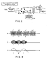
- the digital data is passed through an encoder 10.
- the encoder 10 converts the digital data to an MFM signal or to a Walker encoded signal as will be further explained.
- Walker Encoding is attributable to the invention herein and is a typical way of describing a new encoding technique such as Miller Encoding.
- Miller Encoding or MFM is well known in the art and there are many examples of typical encoding devices which can be employed according to MFM operation for encoder 10.
- the output of the encoder is passed through a RC network 11 which consists of a resistor 12 and a capacitor 13.
- the resistor and capacitor serve as an integrator whereby the output of the encoder is passed through the RC pair to reduce the abruptness of transitions through 0 volts.
- Equal positive and negative swings are applied to a balanced modulator 14 of conventional design.
- Balanced modulators such as modulator 14 are well known in the art. See, for example, a textbook entitled Single Sideband Principles and Circuits by E. W. Pappenfus et al., McGraw-Hill Book Company (1964) Chapter 5 entitled “Balanced Modulators”. It is of course understood that the modulator 14 is sometimes designated as a ring modulator and is employed to create a double sideband suppressed carrier signal with sidebands centered around the frequency determined by the subcarrier oscillator 15.
- the subcarrier oscillator 15 has its output applied to a balancing potentiometer 16 to therefore enable one to adjust the system to null out any residual carrier.
- the techniques for making such a balanced modulator as well as techniques for balancing the same are well known.
- the output of the encoder would be at a 38.4 KB rate with the subcarrier oscillator operating for example at 108 KHZ.
- the signal contains the sidebands which are the carrier frequency plus or minus the envelope frequency of the data, which as indicated in the case of encoded data, relates to the bit rate or baud rate by the factors given above.
- the output also contains sizable third, fifth and higher order harmonics and is therefore quite broad in terms of spectral utilization.
- the output of the transformer or the secondary winding is coupled to an ideal filter 18.
- the filter 18 is a special filter of unique design that has as close to uniform phase shift as possible and a bandwidth as close to that of an ideal filter as possible. It is known and indicated that filters of formal design such as the Butterworth, Chebychev, Synchronous and so on are not suitable for this operation since they do not exhibit uniform phase shift characteristics.
- the bandpass of this filter is one half or less of the frequency spectrum including the carrier frequency and a single sideband. It specifically rejects the carrier and all frequencies below the lowest frequency resulting from encoding, plus all third, fifth and higher harmonics resulting from encoding and modulation.
- FIG. 3A there is shown the data signal which has been modulated by means of the circuit employed in Figure 2 as seen at transformer 17.
- the wave form of Figure 3B is indicative of the wave form obtained after passing through the narrow bandpass filter according to this invention which essentially is shown in Figure 2 as the ideal filter 18. It will not be uniform in amplitude and phase changes occurring at the points between 1, 2 and 3 of Figure 3A will not be exactly 180°. The dips may be as low as 25% of the peak value as shown in Figure 3B. Following FM and PM practice, this envelope can be limited or clipped to remove all noise spikes and variations in amplitude. Such a limited signal would closely resemble Figure 3A with an area of phase confusion between part 1, 2 and 3.
- Figure 5 shows the detector employed to detect the signal generated by the structure of Figure 2.
- the detector shown in Figure 5 is unique in that it utilizes the sideband energy to recreate the original signal, but does not require reconstruction of the carrier to do so.
- the carrier is never required to accurately restore the data and there is no need to worry about carrier frequency, phase or which sideband is being used. In fact, the carrier could well lie within the pass band of another carrier signal when multiple signal channels are employed. This of course results in a great economic benefit to manufacturers and to users of the system.
- the generated RF signal which is the signal shown in Figure 3B is applied to the input of a limiter 20.
- Limiter 20 is a conventional integrated circuit component and essentially will pass a signal exceeding a given amplitude at input 21 depending upon the setting of the gain threshold at input 22.
- the gain threshold setting is conventionally determined by means of a potentiometer 23.
- the output of the limiter is coupled to a phase change detector which is shown in Figure 6.
- the output of the phase change detector is a series of pulses as shown in Fig. 7b which can be decoded by a conventional decoder 25 to obtain the restored NRZ data.
- Such circuits are extremely well known to those skilled in the art. are extremely well known to those skilled in the art.
- phase change detector 24 of Figure 5 Essentially as seen, the RF signal is applied to the limiter 20 as described in conjunction with Figure 5.
- the output of the limiter is applied to an OR gate 26 which has another input obtained from a voltage controlled oscillator or VCO 27.
- the phase comparator and voltage controlled oscillator, or VCO may also be a conventional component such as that supplied by the RCA Corporation and sold under the designation 4046.
- the frequency of the oscillator is controlled by an RC network which is coupled externally to the VCO 27 consisting of a capacitor 28 and a variable resistor 29.
- the VCO is tuned to a lower sideband, which in the example given above is a frequency between the limits of 89 to 97 KHZ, a carrier of 108 KHZ being used, but suppressed.
- the output of the VCO 27 is a square wave at the above-noted selected frequencies.
- the detector as shown in Figure 6 appears to be a conventional phase lock loop, but as will be explained, it is not.
- a conventional phase lock loop detector requires a carrier just as any other conventional single sideband detecting scheme.
- the detector of Figure 6 has no carrier upon which to lock and hence must endeavor to follow the sidebands alone which represent the modulating frequency time periods. Each change in sideband frequency is accompanied by a nearly 180° phase shift.
- the circuit is set to respond within 2 or 3 cycles of the input. Essentially, the circuit does not follow or reproduce the signal envelope, but responds only with a pulse that marks each major phase change.
- the detector is therefore a phase change detector and not a phase lock and loop in the conventional tracking mode.
- Figure 7A there is shown an input RF signal prior to limiting.
- Figure 7B shows the output of the detector, designated as output in the figure 6.
- the output of the phase comparator is applied to a low pass filter and then to a conventional decoder 25 as shown for example in Figure 2 obtain the original NRZ signal.
- the signal of Figure 7B Prior to application of the output of the comparator to the decoder 25, the signal of Figure 7B is applied to an operational amplifier 23 arranged as a clipping circuit to remove noise, where the clipping level is adjustable by means of the potentiometer 24.
- the output of the amplifier 23 is shown in Figure 7C.
- Use of a conventional phase lock loop would result in an output which resembles the output shown in Figure 3C. As one can see from Figure 7B, the output of this detector is completely different.
- This detector is tuned to the sideband filter band pass and does not follow the envelope but essentially creates pulses when the phase changes.
- the RC low pass filter at the output is used to reduce the RF and noise components only.
- the decoder 25 which may be a microprocessor used for MFM or Walker decoding can be constructed to accept a wide variation in the phase change position so that the effects of noise on the limited signal are further minimized.
- the data distortion which results can be corrected in a microprocessor program as will be further explained. This is particularly advantageous when only a few cycles are present between phase changes as in the case when the band rate approaches the carrier frequency.
- a conventional FM or PM detector of the envelope type will cause errors much more easily than the abrupt phase change detector shown in Figure 6, especially in the presence of noise or when only four or five cycles represent a bit of data.
- the detector shown in Figure 6 has employed some of the advantages of the phase lock loop and therefore exhibits some noise immunity. Suitable filtering and limiting, if necessary, can also be used to reduce jitter when the time period of the data approaches that of the carrier frequency.
- the output of the detector is then used to create pulses which are employed by the decoder 25 which then restores the data to its original form (Fig. 1B). It is also indicated that at no time is any effort made to restore the data wave form directly from the RF signal as would be done in a conventional single sideband system.
- Signal reconstruction is implemented by digital means after detecting the almost instantaneous change in phase.
- the filter is made as narrow as possible to accommodate the bandwidth required to transmit a proper signal. Narrowing the bandwidth of the system also results in improvements in signal to noise ratio compared with wider bandwidth systems.
- the filter By employing the filter with the characteristics to be described, one can improve the low level signal to noise ratio by as much as 10 decibels (10 dB.)
- the signal can also be processed by a microprocessor which will handle distortion.
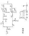
- the filter configuration is shown in Figure 8 and as indicated is extremely critical. Essentially, located below the filter schematic is a typical representation of the band pass K (gain) together with the phase characteristics of the filter which is essentially shown in a conventional format. For the system to function, distant almost 180° phase shifts are required at all frequencies involved. As an example, MFM encoded 19.2 KB data signals will have frequencies ranging from 4.8 KHZ to 9.6 KHZ above and below the carrier frequency. At any point in time, there must be a shift from high to low sideband frequency, or to an intermediate frequency, without losing the 0 to 180° phase shift relationship.
- the filter shown in Figure 8 has been devised to provide 0 phase shift across the pass band while also causing the band pass filter to exhibit a sharper band pass characteristic.
- the filter functions as follows.
- the signal from the modulator which is shown in Figure 2 is passed through the secondary winding of the transformer 17.
- This transformer 17 is coupled via a capacitor 31 to capacitor 30 of Figure 8.
- the capacitor 30 is large in comparison to any capacitor in the resonant circuits. In the case of the circuits shown, it is ten times larger than capacitor 31 and ten times larger than the resonant capacitors 35 and 36.
- This capacitor 30 is shared by two resonant circuits operating at different frequencies and must be large to minimize inter-reaction. A resistor of very low value could also be employed. Any excessive interaction will destroy the filter's phase shift characteristics.
- a first signal path is through a low pass filter consisting of variable inductor 37 and capacitor 36 which are resonated or tuned to an upper frequency limit, for example, which in regard to the embodiment described above, may for example be 95 KHZ.
- a second path is provided through a high pass filter consisting of capacitor 35 in series with variable inductor 38.
- the high pass filter is tuned to the lower frequency limit, which for example may be 93 KHZ.
- a signal larger than that coming from the input source will appear at the input to the amplifiers 40 and 42.
- the gain of the amplifiers is adjusted in a conventional manner by the resistors coupled from input to output as shown in the schematic. This signal level is approximately Q x the incoming signal. Where Q is the quality factor of the resonant circuits.
- the amplifiers 40 and 42 are used to provide very high input impedance to avoid lowering the Q of the resonant circuits. At the same time, the amplifiers provide a very low output impedance to permit resistive mixing of the two signals. The gain of each amplifier is made adjustable to balance the two outputs.
- the amplifiers 40 and 42 are conventional operational amplifiers available in integrated circuit form and sold through many vendors. As indicated, the series circuits as consisting of coil 37 and capacitor 36 and coil 38 with capacitor 35 are stagger tuned and adjusted in Q to provide the desired band width. At frequencies giving a phase shift of more than 45° above and below resonance, the signals at the mixing resistors 41 and 45 are nearly equal in amplitude and cancel in phase.
- the filter is therefore an active filter dependent upon passive circuit elements to function. At frequencies near resonance, with the elements slightly stagger tuned, the phase shifts to ⁇ 90° in the two resonant circuits.
- One op amp 42 inverts its signal, so the signals appear at resistors 41, 45 in phase and adding. As the frequency varies above and below the center, the phase shifts away from in phase, but in opposite directions, i.e., one going positive, the other negative. Since they are added, the effect is to cancel phase shift until the skirt of the filter is reached. Over a narrow range, the two signals are additive and result in a summed output of uniform phase shift (flat phase shift).
- the capacitor 30 is made to be much larger than capacitors 35 and 36 and 31. It is shown that capacitor 30 is ten times larger, but essentially could be 50 or more times larger without affecting the circuit operation.
- the Miller or MFM decoding is a very conventional technique and in fact such decoders can be implemented conventionally by discrete component means.
- MFM encoding can also be accomplished by using a microcontroller or microprocessor chip with an encode/decode program in internal Read Only Memory (ROM). The time between pulses is measured and a computer program determines whether a 1 or 0 has been transmitted.
- the present invention also may employ a unique decoding/encoding method which will be referred to as Walker Encoding and utilizes a narrow bandwidth consistent with good data reliability.
- the method used to accomplish Walker encoding is relatively complex and can be implemented by a microcontroller or microprocessor with the encode/decode program in ROM.
- Figure 9A thus shows a typical clock signal as for example the type of clock signal depicted in regard to Figure 1A.
- Figure 9B shows an NRZ signal which indicates a particular data format.
- Figure 9C depicts the encoding scheme during a reset condition where a previous 1 has been missed.
- Figure 9D shows the encoding scheme from a reset condition where a previous 0 has been missed.
- the rules for formulating such a signal as depicted in Figures 9C and 9D are relatively complicated and will be given as follows. The rules are:
- Figure 9 shows the data encoding according to these rules.
- using the receiver decoders shown in Figure 5 requires a number of carrier cycles to function properly. If the frequency is too low, there will not be a sufficient number of pulses to adequately define the gap or indicate the phase change. Each peak, if missed, results in a displacement to the next peak. For example, if there are 10 cycles in the bit period, missing one will cause a jitter of 10%.
- the detector shown in Figure 6 results in an improvement in this characteristic since it responds to both positive and negative drive.
- the use of a computer program in the microprocessor or microcontroller chip that has wide windows for the timing will further reduce the chance of error. This will be futher explained.
- the system described utilizing the Walker Encoding provides superior operation over conventional communication systems.
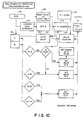
- NRZ data which is obtained from a conventional NRZ source 50 is applied to the input of a shift register 51 and to a leading edge detector 52. It is of course known that circuits for detecting a leading edge of a pulse are well known as circuit 52 while shift register circuits are also well known. Essentially, the NRZ data emanating from source 50 is input to the shift register 51 which holds two bits designated as A and B and which are the present and the last bit. The leading edge of the data is used to reset the counters based on detecting the leading edge via circuit 52.
- the leading edge of the data is used to reset various counters as will be explained.
- a divide by four counter 54 is shown.
- the divide by four counter 54 is reset on each rising edge of the data and is done via the circuit 53 which essentially is a one shot or monostable multivibrator.
- a four times clock is employed which is designated by numeral 55.
- the clock 55 is four times the normal data clock.
- the output of the clock circuit is applied to a delay counter 60 as well as serving as a clock source for the divide by four counter 54.
- the output from the divide by four counter is passed through a delay register 61 where it is used to clock data into the shift register 51 after the input data is stable.
- Various comparator circuits compare the data in the present and the last registers. If the two are the same, the delay counter 60 is set at 4 and the data crossing will occur 4 clock periods later. If they are different, the delay counter is set at 5 and the data crossing occurs 5 counts later. If the delay is A + B indicating a 1, 0 pattern and the counter has one count to go before clocking, the delay counter is set at 6/4 and the divide by four counter is reset at 3 to go before an output.
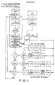
- FIG. 11 there is shown a flow chart indicative of a decode program. It is noted at the onset that the flow chart depicted in Figure 11 can also be implemented by conventional logic circuitry.
- the stack On the start of the program, the stack is cleared. The stack being a microprocessor RAM area designated as stack and three dummy characters are pushed on the stack. This is implemented by modules 70 and 71.
- the program then enters an idle loop waiting period as evidenced by module 72 which essentially waits for incoming pulses. On the first pulse pair spaced 6 clock pulses apart, the program proceeds and essentially the module 72 waits for such a signal. A 6 count indicates that a 1-0 pattern has been sent and the count should be at three counts to go before an output.
- the program sets the count and puts a 1-0 pattern on the stack. This is implemented by modules 73, 74 and 75. Future clocking will output the 1 and the 0 by popping the stack which is a conventional microprocessor technique indicated by module 76.
- a typical stack is 8 bits wide but only one bit is read at the output which is designated by reference numeral 77.
- the program seeks to read the next pulse. If the next pulse is spaced 4/4 period, the software determines the last bit then adds an additional bit of the same polarity. If the count is at 0, a 1 has been missed. Then a 1 is added to the stack in addition to the last bit. If the count is 5, the last bit is recalled, replaced, inverted and added to the stack. If the count is at 0, a 1 has been missed. This previous bit is inverted and replaced on the stack with the missed 1.
- the above-described data system as indicated enables data to be sent at efficiencies of 6 bits per HZ of bandwidth which essentially is also the Nyquist efficiency.
- the system is usable in all radio and cable systems but has applicable use over FM/SCA systems where up to 4 high speed data channels can be transmitted within a single FM station subcarrier space. These channels can be 38.4, 38.4, 19.2 and 19.2 KB channels, offering three times the utilization capability of the SCA spectrum when compared to a standard 38.4 KB FM/FM system with significant improvements in signal to noise.
Landscapes
- Engineering & Computer Science (AREA)
- Computer Networks & Wireless Communication (AREA)
- Signal Processing (AREA)
- Digital Transmission Methods That Use Modulated Carrier Waves (AREA)
Priority Applications (2)
| Application Number | Priority Date | Filing Date | Title |
|---|---|---|---|
| US06/861,049 US4742532A (en) | 1986-05-08 | 1986-05-08 | High speed binary data communication system |
| EP88300355A EP0325005A1 (de) | 1988-01-18 | 1988-01-18 | Hochgeschwindigkeitsübertragungssystem für binäre Daten |
Applications Claiming Priority (1)
| Application Number | Priority Date | Filing Date | Title |
|---|---|---|---|
| EP88300355A EP0325005A1 (de) | 1988-01-18 | 1988-01-18 | Hochgeschwindigkeitsübertragungssystem für binäre Daten |
Publications (1)
| Publication Number | Publication Date |
|---|---|
| EP0325005A1 true EP0325005A1 (de) | 1989-07-26 |
Family
ID=8199923
Family Applications (1)
| Application Number | Title | Priority Date | Filing Date |
|---|---|---|---|
| EP88300355A Withdrawn EP0325005A1 (de) | 1986-05-08 | 1988-01-18 | Hochgeschwindigkeitsübertragungssystem für binäre Daten |
Country Status (1)
| Country | Link |
|---|---|
| EP (1) | EP0325005A1 (de) |
Cited By (3)
| Publication number | Priority date | Publication date | Assignee | Title |
|---|---|---|---|---|
| US7305023B2 (en) * | 2003-07-23 | 2007-12-04 | Intel Corporation | Receivers for cycle encoded signals |
| US7308025B2 (en) * | 2003-07-23 | 2007-12-11 | Intel Corporation | Transmitters providing cycle encoded signals |
| CN108254645A (zh) * | 2018-03-16 | 2018-07-06 | 昆明理工大学 | 一种排阻好坏检测装置 |
Citations (2)
| Publication number | Priority date | Publication date | Assignee | Title |
|---|---|---|---|---|
| US3835386A (en) * | 1972-05-31 | 1974-09-10 | Secr Defence | Binary data communication apparatus |
| US4742532A (en) * | 1986-05-08 | 1988-05-03 | Walker Harold R | High speed binary data communication system |
-
1988
- 1988-01-18 EP EP88300355A patent/EP0325005A1/de not_active Withdrawn
Patent Citations (2)
| Publication number | Priority date | Publication date | Assignee | Title |
|---|---|---|---|---|
| US3835386A (en) * | 1972-05-31 | 1974-09-10 | Secr Defence | Binary data communication apparatus |
| US4742532A (en) * | 1986-05-08 | 1988-05-03 | Walker Harold R | High speed binary data communication system |
Non-Patent Citations (1)
| Title |
|---|
| IBM JOURNAL OF RESEARCH AND DEVELOPMENT, vol. 3, no. 1, January 1959, pages 74-84; New York, US. E. HOPNER: "An experimental modulation-demodulation scheme for high-speed data transmission". * |
Cited By (7)
| Publication number | Priority date | Publication date | Assignee | Title |
|---|---|---|---|---|
| US7305023B2 (en) * | 2003-07-23 | 2007-12-04 | Intel Corporation | Receivers for cycle encoded signals |
| US7308025B2 (en) * | 2003-07-23 | 2007-12-11 | Intel Corporation | Transmitters providing cycle encoded signals |
| US7720159B2 (en) | 2003-07-23 | 2010-05-18 | Intel Corporation | Receivers for cycle encoded signals |
| US8149928B2 (en) | 2003-07-23 | 2012-04-03 | Intel Corporation | Receivers for cycle encoded signals |
| US8559530B2 (en) | 2003-07-23 | 2013-10-15 | Intel Corporation | Transmitters providing cycle encoded signals |
| CN108254645A (zh) * | 2018-03-16 | 2018-07-06 | 昆明理工大学 | 一种排阻好坏检测装置 |
| CN108254645B (zh) * | 2018-03-16 | 2023-09-29 | 昆明理工大学 | 一种排阻好坏检测装置 |
Similar Documents
| Publication | Publication Date | Title |
|---|---|---|
| US4742532A (en) | High speed binary data communication system | |
| US5185765A (en) | High speed data communication system using phase shift key coding | |
| US3818347A (en) | Receiver for amplitude modulated quadrature carrier signals | |
| US6748022B1 (en) | Single sideband suppressed carrier digital communications method and system | |
| US5239672A (en) | Synchronization method and apparatus for simulcast transmission system | |
| US6741646B1 (en) | Modulation technique for transmitting a high data rate signal, and an auxiliary data signal, through a band limited channel | |
| EP1303958B1 (de) | Datenübertragung mittels pulsbreitenmodulation | |
| US4276650A (en) | Method of synchronizing a quadphase receiver and clock synchronization device for carrying out the method | |
| US5053649A (en) | Method and apparatus for high speed phase detection | |
| US5274672A (en) | Optimized clock recovery for an MSK system | |
| US6792051B1 (en) | In-band-on-channel broadcast system for digital data | |
| US4292593A (en) | Method of demodulating a quadphase coded data signal and receiver for carrying out the method | |
| JPS58130658A (ja) | デジタル通信用変調器復調器セツト | |
| JPS6347307B2 (de) | ||
| EP0325005A1 (de) | Hochgeschwindigkeitsübertragungssystem für binäre Daten | |
| US4556869A (en) | Multi-function data signal processing method and apparatus | |
| US4606048A (en) | Radio communication system | |
| US4514697A (en) | Coherent phase shift keyed demodulator with improved sampling apparatus and method | |
| US4577335A (en) | Coherent data communications technique | |
| JPH0542863B2 (de) | ||
| JPS60134545A (ja) | データ通信用信号構造 | |
| GB2029675A (en) | Circuit arrangement for generating sampling pulses for use in receiving stations of data transmission | |
| US3229209A (en) | Vestigial sideband transmission system | |
| Lender | Correlative data transmission with coherent recovery using absolute reference | |
| EP0322038B1 (de) | Digitales Vormodulationsfilter |
Legal Events
| Date | Code | Title | Description |
|---|---|---|---|
| PUAI | Public reference made under article 153(3) epc to a published international application that has entered the european phase |
Free format text: ORIGINAL CODE: 0009012 |
|
| AK | Designated contracting states |
Kind code of ref document: A1 Designated state(s): DE ES FR GB IT NL SE |
|
| 17P | Request for examination filed |
Effective date: 19891120 |
|
| 17Q | First examination report despatched |
Effective date: 19911213 |
|
| STAA | Information on the status of an ep patent application or granted ep patent |
Free format text: STATUS: THE APPLICATION IS DEEMED TO BE WITHDRAWN |
|
| 18D | Application deemed to be withdrawn |
Effective date: 19930817 |