EP0325013A1 - Appareil d'affichage électrophorétique à tableau - Google Patents
Appareil d'affichage électrophorétique à tableau Download PDFInfo
- Publication number
- EP0325013A1 EP0325013A1 EP88300448A EP88300448A EP0325013A1 EP 0325013 A1 EP0325013 A1 EP 0325013A1 EP 88300448 A EP88300448 A EP 88300448A EP 88300448 A EP88300448 A EP 88300448A EP 0325013 A1 EP0325013 A1 EP 0325013A1
- Authority
- EP
- European Patent Office
- Prior art keywords
- conductive lines
- conductor
- selectively
- conductive
- odd
- Prior art date
- Legal status (The legal status is an assumption and is not a legal conclusion. Google has not performed a legal analysis and makes no representation as to the accuracy of the status listed.)
- Granted
Links
- 239000002245 particle Substances 0.000 claims description 22
- 239000012530 fluid Substances 0.000 claims description 8
- 239000006185 dispersion Substances 0.000 claims description 3
- 230000001419 dependent effect Effects 0.000 claims 1
- 239000004020 conductor Substances 0.000 abstract description 244
- 238000000034 method Methods 0.000 abstract description 27
- 230000003111 delayed effect Effects 0.000 abstract description 5
- PXHVJJICTQNCMI-UHFFFAOYSA-N Nickel Chemical compound [Ni] PXHVJJICTQNCMI-UHFFFAOYSA-N 0.000 description 48
- 239000000463 material Substances 0.000 description 29
- 239000011521 glass Substances 0.000 description 24
- 229910052759 nickel Inorganic materials 0.000 description 24
- 229920002120 photoresistant polymer Polymers 0.000 description 23
- 239000000049 pigment Substances 0.000 description 11
- 238000010586 diagram Methods 0.000 description 10
- 238000012937 correction Methods 0.000 description 9
- 238000004519 manufacturing process Methods 0.000 description 8
- 241000283070 Equus zebra Species 0.000 description 6
- 238000005530 etching Methods 0.000 description 6
- 230000000295 complement effect Effects 0.000 description 5
- 238000012545 processing Methods 0.000 description 5
- 230000015572 biosynthetic process Effects 0.000 description 4
- 230000008859 change Effects 0.000 description 4
- 238000011161 development Methods 0.000 description 4
- 238000013508 migration Methods 0.000 description 4
- 230000005012 migration Effects 0.000 description 4
- 239000007787 solid Substances 0.000 description 4
- 230000001360 synchronised effect Effects 0.000 description 4
- 238000007689 inspection Methods 0.000 description 3
- 238000009434 installation Methods 0.000 description 3
- KXGFMDJXCMQABM-UHFFFAOYSA-N 2-methoxy-6-methylphenol Chemical compound [CH]OC1=CC=CC([CH])=C1O KXGFMDJXCMQABM-UHFFFAOYSA-N 0.000 description 2
- 238000003491 array Methods 0.000 description 2
- 230000008901 benefit Effects 0.000 description 2
- 239000011248 coating agent Substances 0.000 description 2
- 238000000576 coating method Methods 0.000 description 2
- 238000013461 design Methods 0.000 description 2
- 230000000694 effects Effects 0.000 description 2
- 230000001747 exhibiting effect Effects 0.000 description 2
- AMGQUBHHOARCQH-UHFFFAOYSA-N indium;oxotin Chemical compound [In].[Sn]=O AMGQUBHHOARCQH-UHFFFAOYSA-N 0.000 description 2
- 238000010422 painting Methods 0.000 description 2
- 239000005011 phenolic resin Substances 0.000 description 2
- 229920001568 phenolic resin Polymers 0.000 description 2
- 238000001259 photo etching Methods 0.000 description 2
- 238000000926 separation method Methods 0.000 description 2
- 238000004544 sputter deposition Methods 0.000 description 2
- LQZFGPJGXVFSTR-UHFFFAOYSA-N 2-[[2-chloro-4-[3-chloro-4-[[1-(2-methylanilino)-1,3-dioxobutan-2-yl]diazenyl]phenyl]phenyl]diazenyl]-n-(2-methylphenyl)-3-oxobutanamide Chemical compound C=1C=CC=C(C)C=1NC(=O)C(C(=O)C)N=NC(C(=C1)Cl)=CC=C1C(C=C1Cl)=CC=C1N=NC(C(C)=O)C(=O)NC1=CC=CC=C1C LQZFGPJGXVFSTR-UHFFFAOYSA-N 0.000 description 1
- 239000004215 Carbon black (E152) Substances 0.000 description 1
- CYTYCFOTNPOANT-UHFFFAOYSA-N Perchloroethylene Chemical group ClC(Cl)=C(Cl)Cl CYTYCFOTNPOANT-UHFFFAOYSA-N 0.000 description 1
- 230000006978 adaptation Effects 0.000 description 1
- 230000002411 adverse Effects 0.000 description 1
- 229910052782 aluminium Inorganic materials 0.000 description 1
- XAGFODPZIPBFFR-UHFFFAOYSA-N aluminium Chemical compound [Al] XAGFODPZIPBFFR-UHFFFAOYSA-N 0.000 description 1
- 238000013459 approach Methods 0.000 description 1
- 125000003118 aryl group Chemical group 0.000 description 1
- 239000003086 colorant Substances 0.000 description 1
- 229930195733 hydrocarbon Natural products 0.000 description 1
- 150000002430 hydrocarbons Chemical class 0.000 description 1
- 239000007788 liquid Substances 0.000 description 1
- 230000013011 mating Effects 0.000 description 1
- 239000011159 matrix material Substances 0.000 description 1
- 229910052751 metal Inorganic materials 0.000 description 1
- 239000002184 metal Substances 0.000 description 1
- 238000012986 modification Methods 0.000 description 1
- 230000004048 modification Effects 0.000 description 1
- 230000008439 repair process Effects 0.000 description 1
- 230000003252 repetitive effect Effects 0.000 description 1
- 230000004044 response Effects 0.000 description 1
- 230000000717 retained effect Effects 0.000 description 1
- 239000000725 suspension Substances 0.000 description 1
- 229950011008 tetrachloroethylene Drugs 0.000 description 1
Images




Classifications
-
- G—PHYSICS
- G09—EDUCATION; CRYPTOGRAPHY; DISPLAY; ADVERTISING; SEALS
- G09G—ARRANGEMENTS OR CIRCUITS FOR CONTROL OF INDICATING DEVICES USING STATIC MEANS TO PRESENT VARIABLE INFORMATION
- G09G3/00—Control arrangements or circuits, of interest only in connection with visual indicators other than cathode-ray tubes
- G09G3/20—Control arrangements or circuits, of interest only in connection with visual indicators other than cathode-ray tubes for presentation of an assembly of a number of characters, e.g. a page, by composing the assembly by combination of individual elements arranged in a matrix no fixed position being assigned to or needed to be assigned to the individual characters or partial characters
- G09G3/34—Control arrangements or circuits, of interest only in connection with visual indicators other than cathode-ray tubes for presentation of an assembly of a number of characters, e.g. a page, by composing the assembly by combination of individual elements arranged in a matrix no fixed position being assigned to or needed to be assigned to the individual characters or partial characters by control of light from an independent source
- G09G3/3433—Control arrangements or circuits, of interest only in connection with visual indicators other than cathode-ray tubes for presentation of an assembly of a number of characters, e.g. a page, by composing the assembly by combination of individual elements arranged in a matrix no fixed position being assigned to or needed to be assigned to the individual characters or partial characters by control of light from an independent source using light modulating elements actuated by an electric field and being other than liquid crystal devices and electrochromic devices
- G09G3/344—Control arrangements or circuits, of interest only in connection with visual indicators other than cathode-ray tubes for presentation of an assembly of a number of characters, e.g. a page, by composing the assembly by combination of individual elements arranged in a matrix no fixed position being assigned to or needed to be assigned to the individual characters or partial characters by control of light from an independent source using light modulating elements actuated by an electric field and being other than liquid crystal devices and electrochromic devices based on particles moving in a fluid or in a gas, e.g. electrophoretic devices
-
- G—PHYSICS
- G02—OPTICS
- G02F—OPTICAL DEVICES OR ARRANGEMENTS FOR THE CONTROL OF LIGHT BY MODIFICATION OF THE OPTICAL PROPERTIES OF THE MEDIA OF THE ELEMENTS INVOLVED THEREIN; NON-LINEAR OPTICS; FREQUENCY-CHANGING OF LIGHT; OPTICAL LOGIC ELEMENTS; OPTICAL ANALOGUE/DIGITAL CONVERTERS
- G02F1/00—Devices or arrangements for the control of the intensity, colour, phase, polarisation or direction of light arriving from an independent light source, e.g. switching, gating or modulating; Non-linear optics
- G02F1/01—Devices or arrangements for the control of the intensity, colour, phase, polarisation or direction of light arriving from an independent light source, e.g. switching, gating or modulating; Non-linear optics for the control of the intensity, phase, polarisation or colour
- G02F1/165—Devices or arrangements for the control of the intensity, colour, phase, polarisation or direction of light arriving from an independent light source, e.g. switching, gating or modulating; Non-linear optics for the control of the intensity, phase, polarisation or colour based on translational movement of particles in a fluid under the influence of an applied field
- G02F1/166—Devices or arrangements for the control of the intensity, colour, phase, polarisation or direction of light arriving from an independent light source, e.g. switching, gating or modulating; Non-linear optics for the control of the intensity, phase, polarisation or colour based on translational movement of particles in a fluid under the influence of an applied field characterised by the electro-optical or magneto-optical effect
- G02F1/167—Devices or arrangements for the control of the intensity, colour, phase, polarisation or direction of light arriving from an independent light source, e.g. switching, gating or modulating; Non-linear optics for the control of the intensity, phase, polarisation or colour based on translational movement of particles in a fluid under the influence of an applied field characterised by the electro-optical or magneto-optical effect by electrophoresis
-
- G—PHYSICS
- G09—EDUCATION; CRYPTOGRAPHY; DISPLAY; ADVERTISING; SEALS
- G09G—ARRANGEMENTS OR CIRCUITS FOR CONTROL OF INDICATING DEVICES USING STATIC MEANS TO PRESENT VARIABLE INFORMATION
- G09G2310/00—Command of the display device
- G09G2310/02—Addressing, scanning or driving the display screen or processing steps related thereto
- G09G2310/0264—Details of driving circuits
- G09G2310/0267—Details of drivers for scan electrodes, other than drivers for liquid crystal, plasma or OLED displays
-
- G—PHYSICS
- G09—EDUCATION; CRYPTOGRAPHY; DISPLAY; ADVERTISING; SEALS
- G09G—ARRANGEMENTS OR CIRCUITS FOR CONTROL OF INDICATING DEVICES USING STATIC MEANS TO PRESENT VARIABLE INFORMATION
- G09G2310/00—Command of the display device
- G09G2310/02—Addressing, scanning or driving the display screen or processing steps related thereto
- G09G2310/0264—Details of driving circuits
- G09G2310/0275—Details of drivers for data electrodes, other than drivers for liquid crystal, plasma or OLED displays, not related to handling digital grey scale data or to communication of data to the pixels by means of a current
-
- G—PHYSICS
- G09—EDUCATION; CRYPTOGRAPHY; DISPLAY; ADVERTISING; SEALS
- G09G—ARRANGEMENTS OR CIRCUITS FOR CONTROL OF INDICATING DEVICES USING STATIC MEANS TO PRESENT VARIABLE INFORMATION
- G09G3/00—Control arrangements or circuits, of interest only in connection with visual indicators other than cathode-ray tubes
- G09G3/20—Control arrangements or circuits, of interest only in connection with visual indicators other than cathode-ray tubes for presentation of an assembly of a number of characters, e.g. a page, by composing the assembly by combination of individual elements arranged in a matrix no fixed position being assigned to or needed to be assigned to the individual characters or partial characters
-
- G—PHYSICS
- G09—EDUCATION; CRYPTOGRAPHY; DISPLAY; ADVERTISING; SEALS
- G09G—ARRANGEMENTS OR CIRCUITS FOR CONTROL OF INDICATING DEVICES USING STATIC MEANS TO PRESENT VARIABLE INFORMATION
- G09G3/00—Control arrangements or circuits, of interest only in connection with visual indicators other than cathode-ray tubes
- G09G3/20—Control arrangements or circuits, of interest only in connection with visual indicators other than cathode-ray tubes for presentation of an assembly of a number of characters, e.g. a page, by composing the assembly by combination of individual elements arranged in a matrix no fixed position being assigned to or needed to be assigned to the individual characters or partial characters
- G09G3/34—Control arrangements or circuits, of interest only in connection with visual indicators other than cathode-ray tubes for presentation of an assembly of a number of characters, e.g. a page, by composing the assembly by combination of individual elements arranged in a matrix no fixed position being assigned to or needed to be assigned to the individual characters or partial characters by control of light from an independent source
- G09G3/3433—Control arrangements or circuits, of interest only in connection with visual indicators other than cathode-ray tubes for presentation of an assembly of a number of characters, e.g. a page, by composing the assembly by combination of individual elements arranged in a matrix no fixed position being assigned to or needed to be assigned to the individual characters or partial characters by control of light from an independent source using light modulating elements actuated by an electric field and being other than liquid crystal devices and electrochromic devices
- G09G3/344—Control arrangements or circuits, of interest only in connection with visual indicators other than cathode-ray tubes for presentation of an assembly of a number of characters, e.g. a page, by composing the assembly by combination of individual elements arranged in a matrix no fixed position being assigned to or needed to be assigned to the individual characters or partial characters by control of light from an independent source using light modulating elements actuated by an electric field and being other than liquid crystal devices and electrochromic devices based on particles moving in a fluid or in a gas, e.g. electrophoretic devices
- G09G3/3446—Control arrangements or circuits, of interest only in connection with visual indicators other than cathode-ray tubes for presentation of an assembly of a number of characters, e.g. a page, by composing the assembly by combination of individual elements arranged in a matrix no fixed position being assigned to or needed to be assigned to the individual characters or partial characters by control of light from an independent source using light modulating elements actuated by an electric field and being other than liquid crystal devices and electrochromic devices based on particles moving in a fluid or in a gas, e.g. electrophoretic devices with more than two electrodes controlling the modulating element
-
- G—PHYSICS
- G09—EDUCATION; CRYPTOGRAPHY; DISPLAY; ADVERTISING; SEALS
- G09G—ARRANGEMENTS OR CIRCUITS FOR CONTROL OF INDICATING DEVICES USING STATIC MEANS TO PRESENT VARIABLE INFORMATION
- G09G5/00—Control arrangements or circuits for visual indicators common to cathode-ray tube indicators and other visual indicators
- G09G5/18—Timing circuits for raster scan displays
Definitions
- This invention relates to electrophoretic display panel apparatus and methods therefor and more particularly electrophoretic display panel apparatus having improved contrast and image alignment.
- the electrophoretic display described therein generally takes the form of a wafer structure formed on a glass sheet generally slightly larger than the size of the panel.
- the glass sheet is coated with indium-tin-oxide (ITO) having a horizontal cathode line pattern etched therein to form horizontal row conductors.
- ITO indium-tin-oxide
- the ITO layer is very thin those of ordinary skill in the art will appreciate that it is relatively transparent.
- An insulating layer formed by photoresist such as phenolic resin impregnated with photoactive material is deposited over the cathode line structure. Thereafter, the photoresist material is overcoated with a nickel layer through the use of sputtering techniques or the like and then the nickel is overcoated by another thin layer of photoresist material.
- a mask having vertically disposed column conductors is placed on the top layer of photoresist and thereafter the wafer formed is exposed to ultraviolet light and developed. Where the photoresist material has been exposed to ultraviolet light the same will be removed leaving vertically disposed columns of photoresist overcoating the nickel layer together with adjacent vertical columns of nickel from which the photoresist has been removed. The nickel is then etched so that nickel material which is not overcoated by photoresist is removed. Subsequently, the wafer structure is flooded with ultraviolet light and again developed so that the vertical layers of photoresist overlying the remaining vertical strips of nickel are removed.
- the wafer is placed in a plasma etcher which effectively removes all photoresist material which is not overcoated by nickel so that columns of vertically disposed nickel conductors which act as grids in the triode structure being formed remain. If a panel display having dimensions of 8 1/2 x 11 inch and a resolution of 200 lines per inch is again considered it will be appreciated that 1,700 vertical columns consisting of 1,700 grid lines are required.
- the electrophoretic display panel being formed is configured to correspond in size to a normal page such as here indicated as comprising an 8 1/2 x 11 inch display and exhibits high resolution characteristics such as a 200 line per inch level described in U.S. Patent Application Serial No. 670,571.
- a normal page such as here indicated as comprising an 8 1/2 x 11 inch display and exhibits high resolution characteristics such as a 200 line per inch level described in U.S. Patent Application Serial No. 670,571.
- 2,200 horizontal row conductors and 1,700 vertical column conductors are employed in forming the cathode grid matrix and hence appropriate alignment at the 3,740,000 intersections which result can be a substantial problem.
- the electrophoretic panel is completed by forming an enclosing anode structure which may typically be formed of ITO in such a manner as described in connection with U.S. Patent Application Serial No. 670,571.
- the anode structure encloses the cathode-grid structure described above and provides an area in which a fluid containing appropriate electrophoretic pigment particles which have been charged may be enclosed. Thereafter, charged pigment particles dispersed in a dielectric fluid to form an electrophoretic dispersion are inserted into the cell and the resulting structure is enclosed within a frame or the like through which electrical connection to the individual grid and cathode conductors is provided.
- connection pads are provided within the frame employed to house the panel and provide electrical connection thereto. Interconnection of pads on the frame and on the panel may be conveniently supplied through the use of Zebra strips or the like as the same readily avoids shorting.
- etching or painting indicia on the panel and frame and providing an assembly fixture therefor would impose a requirement that such fixture include precise optics to preform the required alignment so that such a fixture could not be utilized in the field and would be disproportionately costly in a manufacturing environment.
- An object of one aspect of this invention is to provide electrphoretic display panel apparatus having improved contrast characteristics and methods for allowing the contrast exhibited by such panels to be optimized.
- An object of a further aspect of the present invention is to provide electrophoretic display panel apparatus and methods therefor wherein individual grid electrode structure is tined in appearance and permits the formation of reservoirs for electrophoretic particles intermediate such tines.
- An object of another aspect of the present invention is to provide electrophoretic display panel apparatus having an adjustable delay line structure which is operable to correct misalignment of the panel within a mounting frame or the like.
- An object of yet another aspect of the present invention is to provide electrophoretic display panel apparatus and methods therefor wherein each grid electrode includes a plurality of parallel conductors in the form of tines so that appropriate intersections with cathode conductors will occur even if minor misalignment between an array of row conductors in the form of cathodes and an array of grid electrodes occurs.
- An object of a yet further aspect of the instant invention is to provide electrophoretic display panel apparatus and methods therefor wherein the grid electrodes take the form of a plurality of parallel tines each tine having width characteristics which may selectively vary to optimize contrast conditions exhibited by the display apparatus.
- electrophoretic display panel apparatus having improved alignment and contrast characteristics and methods therefor are provided wherein, according to a first aspect of the invention a display panel having a plurality of rows of cathodes and a plurality of perpendicularly disposed grid conductors are provided and each grid conductor is formed as a plurality of commonly connected parallely disposed lines formed on an insulating tine structure to enable the thickness of each conductor and tine to be adjusted for optimum contrast characteristics and ensure that the requisite number of intersections are provided between rows and columns even should slight misalignment therebetween occur; and according to a second aspect of the instant invention the resulting display panel is mounted in a frame having connecting pads corresponding to similarly disposed pads associated with each column and row conductor within the panel formed to enable connected therebetween to be achieved; however, electrical connections for the conductive pads within the frame are provided through selectively actuatable delay means so that if misalignment between a column or row conductor and a corresponding pad within the frame occurs a signal applied
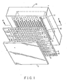
- the electrophoretic display panel apparatus illustrated in Figure 1 comprises a glass plate 2, a plurality of row conductors 4 having contact pads 6, a photoresist layer 8, a plurality of column conductors 10 having contact pads 12 and an anode 14.
- the exploded view of the electrophoretic display panel apparatus illustrated in Figure 1 has been shown substantially out of scale for purposes of illustrating the wafer arrangement formed and in similar manner the presence of the photoresistive layer 8 has been simply shown in Figure 1 as a layer of material to facilitate ease of illustration.
- Figure 3 is a front view, partially in section, illustrating a portion of the electrophoretic display panel apparatus shown in Figure 1 while Figure 4 is an enlarged top view showing an exemplary one of the plurality of column conductors 10 and contact pads 12.
- the glass plate 2 acts to provide a port through which a view of the display may discern image information set forth thereon.
- the glass plate 2 is preferably coated with an extremely thin layer of indium-tin-oxide (ITO) as available as described in the aforesaid U.S. Patent Application Serial No. 670,571 from many suppliers.
- ITO indium-tin-oxide
- the layer of ITO is relatively thin approximately in the range of 300 angstroms in thickness so that the glass plate 2 retains its relatively transparent characteristics.
- the plurality of row conductors 4 and their associated contact pads 6 while illustrated in the exploded view of Figure 1 as residing on the photoresist layer 8 are in fact best shown in Figure 3 as etched from the ITO layer overcoated on the glass plate 2.
- the glass plate 2 bearing the ITO layer may be initially overcoated with a photoresistive layer of any conventional form and thereafter a mask having the conductor pattern associated with the plurality of row conductors 4 and contact pads 6 is placed on the photoresistive layer formed.
- the glass plate is then exposed to ultraviolet light through the mask and developed. What remains will be a conductor pattern corresponding to that illustrated in Figure 1 for the plurality of row conductors 4 and the contact pads 6 wherein each conductor and pad will be overcoated by photoresistive material.
- the remaining ITO will be exposed in that the same will not be overcoated with photoresistive material.
- the ITO layer may be etched using conventional etching techniques so that only ITO material overcoated by photoresistive material which corresponds to the mask employed in the exposure step remains. Thereafter, the entire glass plate 2 is again exposed to ultraviolet light without the benefit of the mask so that the photoresistive material on top of the ITO row conductor pattern formed, as shown in Figure 1, is now exposed. Upon development, this photoresistive material is removed leaving the plurality of row conductors 4 having contact pads 6 illustrated in Figure 1 on the backside of the glass plate 2. Inspection of Figure 3 will readily reveal that this conductor pattern is effectively formed on the back of the glass plate 2 rather than on the layer of photoresistive material 8 illustrated in Figure 1.
- the electrophoretic display panel apparatus described herein is a triode type device employing discrete cathode, grid, and anode structure.
- a triode form of the device is preferred since use of independent grid structures allows a ready threshhold to be established which enables electrophoretic particles which are charged to displace to and from wells formed at the intersection, as shall be seen below, of the cathode and grid structures toward and away from the anode 14.
- the plurality of row conductors 4 and their contact pads 6 are utilized herein as cathode elements which are selectively provided with a potential of approximately 0 volts when the row defined thereby is to be written.
- the single row conductor 4 defining a row to be written is referenced to zero potential causing electrophoretic material to propagate toward or away from the wells associated with each intersection of that row with each column driver depending upon whether or not a 1 or a 0, i.e. +7.5 volts or -7.5 volts is applied to the column driver in question.
- the electrophoretic materials as more fully described in U.S. Patent Application Serial No. 670,571, are pigment particles having a different color than the fluid within the electrphoretic display panel.
- the electrophoretic display panel apparatus illustrated in Figure 1 is similarly configured to be a high resolution 8 1/2 x 11 inch display of the type described in the aforesaid U.S. Patent Application Serial No. 670,571 and for this reason a portion of the glass plate 2 upon which image information is displayed will exhibit an active area of approximately 8 1/2 x 11 inches.
- the display illustrated in Figure 1 is also a high resolution display of the type described in U.S. Patent Application Serial No. 670,571 and employs each of the materials and basic modes of electrophoretic operation described therein. This means that the display illustrated in Figure 1 will exhibit resolution of 200 lines per inch. Hence while only a relatively few row conductors 4 and their associated pads 6 are illustrated in Figure 1, those of ordinary skill in the art will appreciate that assuming the active are of the display is 8 1/2 inches wide and 11 inches long there will be 2,200 horizontally disposed cathode or row conductors 4 etched on the back surface of the glass plate 2.
- connection pads 6 for each row are brought out to opposite sides of the display such that contact pads for rows 1, 3, 5...2199 are brought out to the right side of the display while contact pads 2, 4, 6...2200 are brought out to the left side of the display.
- this interleaving of the connection pads 6 for the row conductors is done for the practical purpose of increasing connection space on the display and should a smaller number of row or cathode conductors be involved such interleaving would be unnecessary.
- resolution of 200 lines per inch is viewed as highly desirable since the same at least equals or exceeds the majority of CRT displays available today, specific resolution characteristics set forth may be varied to suit the choice of the designer.
- each of the row conductors 4 formed from the 300 angstrom coating of ITO was typically of the order of 112 um while separation between adjacent row conductors was 15 um.
- the length of each row conductor was typically 9 inches and each of the pads 6 took the form of a rectangle having dimensions of 3/8 of an ich by .005 of an inch. Quarter inch spacing was also provided between the end of each row conductor and the connection pad 6 associated with the adjacent row conductor.
- contact pads 6 illustrated in Figure 1 are shown on the photoresistive layer 8, the same in fact are preferably not overcoated with photoresistive material and are left exposed in the manner clearly shown in Figure 3 so that the same are available for connection without processing to remove photoresistive material.
- the photoresistive material may typically take the form of phenolic resin impregnated with photoactive material.
- the photoresistive layer 8 is overcoated with a thin layer of nickel in the same manner described in connection with U.S. Patent Application Serial No. 670,571 and it is from this layer that the plurality of vertical conductors 10 and associated contact pads 12 are formed.
- the thin layer of nickel overcoated on the photoresistive layer 8 may be formed using conventional sputtering techniques well-known to those of ordinary skill in the art.
- a second photoresistive layer is formed over the nickel so that the plurality of vertically disposed conductors 10 which form grid electrodes and their associated contact pads 12 may be formed through conventional etching techniques.
- each of the colum conductors 10 and their associated pads 12 will take the form of a tine like structure typically illustrated in Figure 4 which shows an exemplary tine column conductor structure according to the instant invention. More particularly, each column conductor as best seen in Figure 4 will comprise contact portion 12 which may be dimensioned in a manner which corresponds to the dimensions of the contact portion 6 or, alternatively, any other convenient dimension may be employed.
- the structure here employed for the column conductors 10 takes the form of a plurality of parallel conductor members 16 shown in Figure 4 which are connected in parallel by the contact pad 12 and an interconnecting conductor portion 18.
- four individual parallel conductor members 16 for each column conductor have been illustrated; however, those of ordinary skill in the art will appreciate that a greater or lesser number of parallel conductor members may be employed to facilitate design requirements and, more particularly, the contrast requirements of the display being designed due to the presence of the wells established.
- grid conductors 10 having multiple conductor memebrs 16 is viewed as highly advantageous for two basic reasons. The first is that, as shall be seen below, wells for electrophoretic material are established between the conductor memebrs 16 as well as about the periphery. This means, as will be appreciated by those of ordinary skill in the art, that displays provided with such grid structure may be designed to exhibit desired contrast characteristics. This occurs since the nickel conductor members employed will not change color when electrophoretic material is present or removed from the well and hence the thicker the grid member 10 is the less contrast will be exhibited. However, those of ordinary skill in the art will appreciate that in the areas of intersection a substantial voltage gradient must be established to cause the electrophoretic pigment particles to migrate from and to wells established.
- each conductor member 16 employed in a given column conductor 10 had a width of from 10-15 um while the spacing therebetween was typically 20 um.
- the length of each conductor member 16 was typically 11 3/8 inches it being noted that the interconnecting contact portion 18 had a length of 112 um and a height of approximately 1/8 of an inch.
- the plurality of column conductors 10 having contact pads 12 are formed in the nickel layer sputtered on the photoresistive layer 8 in much the same way as the row conductors 4 were formed. More particularly, a mask having the column conductor pattern illustrated in Figure 1 is placed on top of the photoresistive-nickel-photoresistive wafer previously described as formed on top of the row conductors 4. The sandwich is then exposed to ultraviolet light through the mask and developed. This will cause portions of the photoresistive layer overlying the nickel to be removed in areas where the mask is not present. Thus, the column conductor pattern illustrated in Figure 1 is formed with photoresistive material overlying the contact pads 12 and each of the conductor memebrs 16 within each conductor 10.
- the nickel is then etched so that all portions of the nickel layer not covered by photoresist are removed. This will then leave the conductor pattern illustrated in Figure 1 for the vertical conductors 10 present wherein each conductor 10 and pad 12 is covered with photoresist overlying a nickel layer which in turn overlies a layer of photoresist while other areas have only the original photoresist layer 8 remaining.
- the original photoresist layer 8 it may be noted, will have been hardened after the same was applied so that the same will not be removed by standard development techniques. Once this has occurred the surface is flooded with ultraviolet light and developed so that the photoresist overlying the nickel which remains is removed.
- each of the 4 tines 16 and the contact pad 12 of the column conductor formed of nickel is mounted on corresponding tines 20 of photoresistive material formed of the layer 8 and each contact pad 12 resides on corresponding size portion of photoresist 8.
- a section hs been taken through AA to better show the tine arrangement formed.
- a well is effectively formed at the surface of each row conductor 4 intermediate each tine of photoresistive 20 underlying a conductor member 16 as well as adjacent thereto. Exemplary well locations for electrophoretic material are illustrated in Figure 3 by the reference numerals 22.
- the anode structure 14 as illustrated in Figures 1 and 3 may take the form of glass plate or the like which is coated with ITO material.
- the anode is shown curving down to the surface associated with the row conductor 4, however, those of ordinary skill in the art will appreciate that it is only the inner surface of the anode 14 which is parallel to the array of column and row conductors that is made conductive while the side surfaces thereof are not conductive nor energized and are employed solely for the purpose of providing a fluid tight chamber above the electrodes.
- essentially a hollow cavity 24 is formed over the row and column electrodes 4 and 10 for purposes of retaining electophoretic pigment particles disposed within a suitable fluid medium which is preferably dielectric in character. More particularly, once the anode 14 is formed on the display panel, the cavity 24 is filled with an electrophoretic suspension which comprises any of the dielectric liquids and charged electrophoretic particles described in U.S. Patent Application Serial No. 670,571.
- a typical solution which has proved to be highly advantageous comprises 4% of AAOT yellow, .16% of CENTROLEX P, 80.51% of tetrachloroethylene and 15.3% of a hydrocarbon such as Aromatic 150 sold and distributed by Exxon Company and .03% of Sudan Black dye.
- a hydrocarbon such as Aromatic 150 sold and distributed by Exxon Company and .03% of Sudan Black dye.
- the display will appear dark grey except at locations where charge is impressed. In these regions graphic yellow image portions upon a black or dark grey background will be formed providing a bright, effective and clear display.
- the display may be formed either at the glass associated with the cathode or that of the anode depending upon the nature of the charges impressed on the electrophoretic particles.
- Fluid tight enclosure 24 may be formed by the anode through conventional bonding techniques well-known to those of ordinary skill in the art.
- the electrophoretic display panel apparatus may be mounted in a frame structure in which the same is securely retained.
- the frame structure will typically contain contact pads for supplying electrical signals to the contact pads 6 and 12 on the display together will conventional interface and control logic for supplying image formation obtained, for instance, from a character generator ROM in a word processing station or the like to the display.
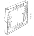
- FIG. 2 there is shown a pictorial view illustrating frame structure suitable for mounting the electrophoretic display panel apparatus shown in Figure 1 and, more particularly, the arrangement of contact pads therein.
- the contact pads per se have been illustrated so that a reader hereof will be fully aprised of alignment problems which typically occur in mounting display panels of the type illustrated in Figure 1.
- Interface and logic components such as shown in Figures 5, 6 and 8 herein which are normally included within such a frame structure as illustrated in Figure 2 have not been shown therein to simplify the illustration set forth.
- Those of ordinary skill in the art will appreciate that the same when normally incorporated are on conventional logic boards and may be mounted in a convenient manner within the frame of a separate structure.
- the frame structure illustrated in Figure 2 comprises a frame structure 30 which may be formed of metal, plastic or the like and have the look of a conventional picture frame such as the modern aluminum picture frames employed for photographs or the like.
- the frame will have an internal cut-out 32 corresponding to a dimension of 8 1/2 x 11 inches or that corresponding to the anode 14.
- Mounted about the rectangular periphery internal to the frame are a pair of rows 34 and 36 of contact pads for the column conductors 12 for the display panel illustrated in Figure 1 and a pair of columns 38 and 40 of contact pads for the row contact pads 6 for the display illustrated in Figure 1.
- rows 34 and 36 shall each contain 850 contact pads; row 34 containing contact pads for the odd column conductors brought out at the top of the display while row 36 contains 850 contact pads assigned, as indicated to the even contact columns brought out at the bottom of the display.
- each column of contact pads 38 and 40 will have 1,100 contact pads wherein 1,100 contact pads in column 38 are assigned for connection to the 1,100 odd contact pads 6 brought out to the right of the display panel illustrated in Figure 1 while the column of contact pads 40 will have 1,100 contact pads assigned respectively to the evenly numbered contact pads 6 brought out to the left of the display illustrated in Figure 1.
- the odd and even assignment of the contact pads in rows 34 and 36 has been indicated in Figure 2 as has the odd and the even assigned contact pads within columns 38 and 40.
- column information in the form of 1's and 0's are loaded into a 1,700 bit latch arrangement formed by a pair of 850 bit, odd and even latches whereupon all 1,700 bits are simultaneously applied to corresponding ones of the 1,700 contact pads within the rows 34 and 36 of the frame.
- the same time loading takes place the single contact pad in columns 38 and 40 associated with the complete row of information being written is energized. If this information is appropriately applied to corresponding contact pads 6 and 12 on the display illustrated in Figure 1 an appropriate row of information will be written on to the display. This will be continued until all 2,200 rows of the display have been written. Since the migration of electrophoretic particles will remain until the display is erased there is no need for a refreshing of the display until new information is to be written.
- FIG. 5 there is shown a block diagram schematically illustrating a portion of an exemplary embodiment of column driver circuitry suitable for supplying data to the column conductors 10 employed within the instant invention by way of applying 850 bits of column information to each of the contact pads in rows 34 and 36 of the contact pads on the frame 30. Since the circuitry illustrated in Figure 5 is configured in a repetitive manner only circuitry for the odd contact pads in row 34 is illustrated it being appreciated by those of ordinary skill in the art, with the minor exception noted in the description thereof, identical circuitry would be employed for the even contact pads present in row 36 in Figure 2.
- the column driver circuitry illustrated in Figure 5 comprises an 850 bit serial in, parallel out shift register 44, 850 latches 46 and 850 AND gates 481-48850.
- the 850 bit serial in, parallel out shift register 44 may be formed by interconnecting a plurality of 64 bit, 32 bit, serial in, parallel out shift registers or a combination thereof until an 850 bit shift register configuration is obtained.
- 13, 64 bit and 1 32 bit shift register chips could be interconnected in such a manner that the Data Output of a preceding shift register is interconnected to the Data Input of the next shift register in sequence while the Clock and Clear inputs are connected in parallel.
- the set inputs thereto may also be connected in parallel, however, in the usual case it is only the set input of the first shift register chip which is utilized to set a 1 into the initial stage thereof after the same has been cleared and hence parallel connection of this input is not usually required.
- the Data In input is connected to conductor 50 in the manner indicated and would receive 1,700 bits of serial information representing dot information as would be typically generated by the character generator ROM employed within a word processing station or other processor to which the display being driven is connected.
- the line is typically assembled by the processor and supplied a character at a time to a character generator ROM which will output appropriate dot information thereof.
- the character generator ROM will produce bits of dot or no dot information for each character in the line of information provided and this information plus appropriate spacing information will typically be assembled in a shift register and output serially to the display which in this case would be the Data In input connected to conductor 50.
- the character generator ROM 7 lines of dot or no dot information will be output for each character and line information corresponding to the entire line of ASCII code supplied to the character generator ROM will be supplied to the display one line at a time.
- the terminal annotated Data Out which is connected through conductor 52 to the shift register 44 takes the form of a conventional overflow or Data Out output of a shift register.
- the data output of each register chip except for the last would be connected to the Data In input of the following shift register chip so that a series chain for that data being clocked through the devices is established in a manner well-known to those of ordinary skill in the art.
- a 1 is written into the first bit position of the first shift register chip the Data Out output of the last stage thereof may be monitored and when a 1 output is shifted therefrom the same may be employed to indicate that the 850 bit shift register 44 has been fully loaded. Hence the presence of the 1 output may be employed to generate an enable level or other strobe signal.
- the Clock 1 input connected to conductor 54 is developed from the circuit illustrated in Figure 6.
- 850 clock pulses are generated thereby in response to a system data clock which effectively generates 1,700 clock pulses.
- the Clock 1 pulses are timed to occur during the presence of the 850 odd bits of data present in the 1,700 bit data stream supplied to the Data In input 50.
- alternate bits of data present in the data stream applied to conductor 50 which correspond to the 850 odd data bits therein are serially clocked into the shift register 44 so that upon the expiration of 850 clock pulses the shift register 44 will be loaded with the 850 odd bits of data within the data stream.
- a Clock 2 input also generated in Figure 6 is utilized.
- the Clock 2 input as shall be seen below generates 850 synchronously timed clock pulses which correspond to the presence of the 850 even bits of data presentin the 1,700 bit data stream supplied to the Data In input of the 850 bit shift register employed for the evenly designated connector pads in row 36.
- the data need not be separated for the application to the odd and even column connector pads in rows 34 and 36 in Figure 2 and similarly separate connection from a 1,700 bit driver arrangement is not necessary.
- the Clear input to the shift register 44 which is connected to conductor 56 is employed to clear the shift register 44 each time 850 bits of odd column information have been written into the shift register 44 and subsequently loaded in parallel into the 850 latches 46. Thereafter, while the latches 46 are being read, new column information may be clocked into the 850 bit shift register 44 so that information may be written into the shift register 44 and read from the latches 46 in a flip flopped or alternating manner well-known to those of ordinary skill in the art.
- the Set input to the 850 bit shift register 44 connected on conductor 48 is not generally employed except, for the purpose of writing an initializing 1 into stage one of the first shift register in the 850 bit shift register 44 or for diagnostic purposes which are not here relevant.
- the output of the 850 bit shift register 44 is applied in parallel though conductors 601-60850 to the individual latches within the 850 latch array 46.
- the operation of the shift register 44 is that the same is cleared subsequent to the gating of information therefrom into the 850 latch array 46. This is done by the application of a clear pulse to a conductor 56. Once clearing has occurred a 1 may be written into the initial stage thereof by the application of a 1 level to the set input thereof and thereafter data and clock signals on conductors 50 and 54 are awaited. More particularly, serial data is applied to conductor 50 in the manner aforesaid so that a serial stream of 1,700 bits is applied thereto.
- Clock 1 pulses are applied to conductor 54 in such a manner that 850 clock pulses timed to occur during the presence of the odd data pulses within the data stream are applied to conductor 54. This will cause, in a manner well-known to those of ordinary skill in the art, the odd data pulses present in the serial data stream applied to conductor 50 to be clocked through the 850 bit storage locations within the shift register 44 in a serial manner.
- the shift register 44 may be cleared to await a next group of 850 bits of information associated with the next 1,700 bits of data for the row within the display. It will also be appreciated that what has just been described for the odd column driver array shown in Figure 5 will also be occuring with respect to the even column driver array, not shown, under the auspices of the Clock 2 clocking signal.
- the latch array 46 may comprise 850 individual latches or alternatively a plurality of multi-latch chips may be employed. In either case the latch input to each chip is connected in parallel to conductor 62.
- Each of the latches act in the manner well-known to those of ordinary skill in the art to load any data supplied to the inputs thereto on conductors 601-60850 during the presence of a latching pulse on conductor 62.
- each of AND gates 481-48850 acts in a manner well-known to those of ordinary skill in the art to produce a high at the outputs thereof only when both of the inputs thereto are high and only for the duration of such high inputs. Therefore, it will be appreciated that when a high level is applied to the strobe conductor 66 whatever input is supplied to the AND gates 481-48850 on conductors 641-64850 is applied to the outputs of the AND gates and for the duration of the strobe pulse.
- the outputs of each of the AND gates 481-48850 as indicated by the terminal annotations C1-C1699 are connected to the odd column connector pads disposed within the row of connector pads 34 illustrated in Figure 2.
- Each 1,100 bit shift register may be clocked in an alternate manner each time the column driver arrangement for the odd and even columns as shown in Figure 5 in enabled or strobed and the 1,100 bit latches thereof are strobed in an alternate manner when the 1,700 bit column latches are strobed.
- a row is written when a 0 volt level is applied to a row conductor 4 and 1 and 0 information is present on all 1,700 column lines 10.
- FIG. 6 there is shown a block diagram schematically illustrating an exemplary embodiment of a circuit suitable for separating data between odd and even columns.
- the circuit illustrated in Figure 6 serves to generate the Clock1 input described in connection with Figure 5 as well as a Clock2 input which would be employed in a circuit identical to that illustration in Figure 5 to drive even columns C2, C4, C6 . . . C1700.
- the use of separate odd and even driver circuits such as illustrated in Figure 5 is preferred in order to permit installation of such driver circuits in association with the odd and even column connection pads illustrated in Figure 2.
- the circuit of Figure 5 may be replaced by a 1700 bit arrangement and under these circumstances direct connection to odd and even connection pads could be implemented. This of course would avoid the need for the use of the exemplary embodiment of a circuit for separating data between odd and even columns as illustrated in Figure 6
- the function of the exemplary circuit illustrated in Figure 6 is to separate a stream of data clock pulses into two streams of clock pulses herein designated Clock1 and Clock2 which represent the odd and even clock pulses respectively within the stream of data clock pulses.
- Data clock pulses as shall be seen in greater detail below are pulses which are synchronized to the system clock and correspond in width thereto. However, the same represent a burst of pulses which are synchronized to the beginning of data to be written and have a fixed length corresponding to the number of bits to be written. Thus under the circumstances here being described data clock pulses will correspond in number to 1700, the number of column bits written in each row.
- the exemplary embodiment of a circuit suitable for separating data between odd and even columns illustrated in Figure 6 comprises first and second flip flops 70 and 72, a plurality of inverters 74 and 78, NAND gates 80 and 82 and an OR gate 84 whose inputs are inverted.
- the flip flops 70 and 72 may take the form of conventional D type flip flops which act in the conventional manner to present the logic condition applied at the D input thereto to its Q output whenever a clock pulse is applied during the presence of such D input. The complementary condition is maintained at the Q Not output.
- the clear input to each of the flip flops 70 and 72 is connected as indicated through conductors 86 and 88 to a system reset.
- each of the flip flops 70 and 72 is connected through conductors 90 and 92 to the Q Not or complementary output present at that flip flop.
- the Q output of each of the flip flops 70 and 72 is connected through conductors 94 and 96, respectively, to one input of a NAND gate 80 or 82 associated therewith.
- the exemplary clock pulse separation circuit illustrated in Figure 6 is highly symmetrical.
- the clock input to the flip flop 70 is connected through a conductor 98 to an input annotated DACLK bar or the Data Clock Not input which represents the inverted data clock.
- the data clock corresponds to the system clock in frequency, pulsewidth and polarity; however, the number of pulses present therein is limited to the number of bits to be written into the column drivers or in the case being discussed 1700.
- the data clock may be conveniently developed by ANDing the system clock with the output of a counter. This data clock is then inverted through the use of a conventional inverter in order that negatively directed clock pulses appropriate for switching the D flip flops 70 and 72 are obtained.
- the data clock input on conductor 98 is also supplied through conductor 100 to the inverters 74.
- the inverter 74 may take the conventional form of an inverter device which acts to produce a complement of an input at the output thereof and is here employed to ensure appropriate timing.
- the inverter 74 produces a complementary clocking level at it's output.
- the output of inverter 74 is applied through the conductor 102 to a second input of the NAND gate 80.
- the NAND gate 80 acts in the conventional manner to produce a low at the output thereof on conductor 104 when both of the inputs thereto are high.
- the output of NAND gate 80 will go low on conductor 104; however, when either input to NAND gate 80 is low the output on conductor 104 will be high.
- the output of the NAND gate 80 on conductor 104 is directly applied through conductor 106 to the terminal annotated clock1 which is a signal directly employed in Figure 5 as a aforesaid.
- a negative pulse will be produced on conductor 106 to correspond with the presence of the first, third, fifth . . . .1699th clock pulses within the data clock.
- the output of NAND gate 80 as present on conductor 104 is also applied as indicated in Figure 6 to one input of the OR gate 84 whose inputs are inverted.
- the OR gate 84 acts in the conventional manner of this well known class of device to produce a high at the output thereof on conductor 108 only when one of the inputs thereto is low.
- the output of OR gate 84 as supplied on conductor 108 is employed to generate the clock input for the second flip flop 72 after the same is inverted by the inverter 78 in the manner plainly illustrated in Figure 6. It will be appreciated that each time the clock1 output on conductor 106 goes high or terminates the output of OR gate 84 will go low and after inversion by the inverter 78 will effectively act as a clock input to the second flip flop 72.
- This means that the Q Not output of flip flop 72 as supplied to the D input thereof on conductor 92 is clocked into the Q2 output thereof on conductor 96 when the Clock1 output goes high or terminates.
- a second input to the OR gate 84 is supplied through conductor 110 from the output of the NAND gate 82 on conductor 112.
- This output of the NAND gate 82 corresponds to the Clock2 output of the circuit or the clock output which comprises even pulses 2, 4, 6 . . . 1700 as present within the data clock.
- the NAND gate 82 whose output on conductor 112 is employed to generate the Clock2 signal acts in the well known manner to produce a low at the output thereof on conductor 112 whenever both inputs thereto are high.
- the first input to NAND gate 82 is supplied, as aforesaid, through conductor 96 from the Q output of flip flop 72.
- the second input to NAND gate 82 is connected through conductor 114 from the system clock as indicated in Figure 6.
- this input on conductor 96 to NAND gate 82 is gated by the system clock applied on conductor 114.
- conductor 96 is primed at the termination of the Clock 1 input, the output of NAND gate 82 will not go low until the next clock signal is produced by the system clock, which is synchronized with the data clock, on conductor 114.
- it is during this interval of the system clock which is an even pulse that the output on conductor 112 which generates Clock2 will go low.
- the circuit illustrated in Figure 6 will supply odd numbered clock pulses within the data clock at it's Clock1 output while even numbered clock pulses present in the data clock are applied to the Clock2 output thereof.
- Each clock signal present at the Clock1 and Clock2 outputs thereof are negative going clock pulses which correspond in duration to the clock pulse present in the data clock and system clock.
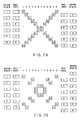
- Figure 7A shows an illustrative diagram of a portion of a display under conditions of proper alignment of the contact pads on the electrophoretic display panel apparatus shown in Figure 1 with the contact pads on the frame shown in Figure 2. More particularly, as shown in Figure 7A, it is assumed that an X is being displayed on a portion of the display panel illustrated in Figure 1 controlled by data supplied to column conductors 1-12 and row conductors 1-12. It will be appreciated that the X will be properly displayed when the rows and columns are connected in the manner illustrated in Figure 7A.
- Figure 7B treats a case of simple misalignment in that while all of the row pads in the odd columns disposed along the left hand portion of the figure are properly aligned, a simple misalignment of one row has occured along the right hand set of pads so that as illustrated in Figure 7B frame pad for row 4 is connected to display pad for row 2 and such misalignment by one row is continued.
- the X which should have been displayed is highly distorted for the simple misalignment condition being considered.
- perfect alignment is much more difficult to obtain and it is not at all infrequent that much time is spent in repositioning the frame structure.
- misalignment by an order of 4 in Figure 7B would result in a much greater case of distortion and of course might well result in misalignment of the columns as well. This of course would produce a rotation of the distorted image.
- misalignment after the assembly of the display within the frame may be simply corrected through electronic means. This is accomplished by effecting a delay in the information applied to the non-misaligned pads which delay corresponds the number of clock pulses associated with the degree of misalignment. Accordingly when correction in this manner is implemented, as shown in Figure 7C, although some loss of information occurs the distorted information being displayed is corrected. Thus, it will be recalled in Figure 7B misalignment of one column had occured resulting in the distorted image of an X shown in Figure 7B. If however the information provided to the rows which are not misaligned, i.e.
- FIG 8 there is shown an illustrative block diagram of an exemplary alignment correction circuit in accordance with the teachings of the instant invention and more particularly an exemplary circuit for implementing the correction illustrated in Figure 7C or the like.
- the circuit illustrated in Figure 8 is connected for example in series with the data input supplied to the circuit shown in Figure 5 for the odd column connectors and receives its input from the data stream normally applied to the Data In input on conductor 50 as illustrated in Figure 5. It is envisioned that one circuit of the type illustrated in Figure 8 shall be applied to each of the odd and even column driver circuits employed with the electrophoretic display panel apparatus according to the instant invention and conversely a circuit of the type illustrated in Figure 8 shall also be applied to each of the odd and even row driver circuits employed.
- the exemplary embodiment of the circuit illustrated in Figure 4 is capable of correcting misalignment problems of the type described in association with Figure 7A-7C for up to eight levels of misalignment of the pads associated with an odd or even row or column.
- the circuit of Figure 8 is basically a delay device and hence if the odd rows were misaligned correction would be implemented on the even rows and vise versa and the same situation obtains for the columns.
- the illustrative block diagram of the alignment correction circuit illustrated in Figure 8 comprises eight switches indicated generally by switches D0-D7, eight gating circuits 119-126 and eight flip flops 130-137.
- the circuit is operative to insert one clock cycle of delay into a signal for each switch D0-D7 that is opened while if the switch is left in a closed position no delay is inserted.
- the switches must be opened in numerical order and the circuit receives data on the right and outputs data at the left.
- each of the switches D0-D7 is a single throw switch which connects between ground as shown in its closed position and a junction connected to 5 volts DC through a resistor R1, an input to an associated inverter I0-I7 and one input to an associated one of gate chips 119-126.
- Each of the gate chips 119-126 may comprise a conventional 7451 chip as available from Texas Instrument Corporation or the like. Each of the gate chips 119-126 has been illustrated as comprising a pair of AND gates A1 and A2 and a NOR gate N1 . Each of the AND gates A1 and A2 act in the conventional manner of this well-known class of device to produce a high output only when both of the inputs thereto are high while producing a low when any input thereto is low.
- the NOR gates N1 comprise conventional forms of this well-known class of device and act to produce a low at the output thereof when either of the inputs thereto are high.
- each of the NOR gates N1 are provided from the outputs of the AND gates A1 and A2 within each of gate chips 119-126. Furthermore, each of gate chips 119-126 are provided with inputs in a corresponding manner. The outputs of each gate chip 119-126 as taken from the output of the NOR gate N1, is inverted through one of inverters 140-147 and provided to either the data output of this circuit in the case of inverter 140 or to the flip flop 130-136 associated with the output of that stage.
- Each of the flip flops 130-137 are conventional D-type flip flops which act in the manner described in connection with Figure 6 to assume the level applied to its D input in the presence of a clock pulse.
- the D inputs to each of the flip flops 130-136 are connected to the inverter 141-147 associated with that stage while the D input to flip flop 137 receives the data input to the circuit as indicated by the terminal 150.
- the Clock input to each of the flip flops 130-137 is supplied with a Clock 1 or Clock 2 input provided to the odd or even row or columns to which it is assigned. This clock input is developed in the precise manner as was described in connection with Figure 6.
- the clock input as indicated in Figure 8 is inverted by a pair of conventional inverters 154 and 156 and thereafter applied to the clock input of each of the flip flops 131-136 through the conductor 158.
- the Data In input which, in the case of column drivers, would correspond to the Data In input on conductor 52 in Figure 5 is applied through a pair of inverters 160 and 162 to the D input of the flip flop 137 and one of the inputs to the A1 AND gate present in each of the gate circuits 119-126.
- one circuit such as illustrated in Figure 8 will be provided for each of the odd and even column driver circuits as well as each of the odd and even row driver circuits.
- all the switches D0-D7 in each of the four delay arrays provided will be closed.
- the display will be energized and the operator will note any misalignment problems on the screen. For instance, if a result such as illustrated in Figure 7B occurred, it would be clear that misalignment has occurred with respect to one of the rows present in the even side of the panel. This would require that one switch D0 be closed in the delay array illustrated in Figure 8 assigned to the odd side of the panel so that the correction illustrated in Figure 7C can be obtained. Under these circumstances switch D0 would be opened while all the remaining switches remain closed.
- switches D1-D7 would remain closed while switch D0 would be opened. Under these conditions a high level would be present at one input to AND gate A2 while a low is imposed on the input of AND gate A1 connected to the inverter I0. Hence AND gate A1 is effectively disabled. Under these conditions gate array 120 would be effectively enabled for the receipt of the first bit of data. Therefore, when this bit of data is applied to AND gate A1 which is enabled by a high from the output of inverter I1, the output of AND gate A1 in gate array 120 would go high placing a high at the input to NOR gate N1.
- one aspect of the present invention provides an electrode panel of an electrophoretic display having a first plurality of conductors extending transversely to, insulated from and forming crossing points with a second plurality of conductors, each of at least one of said pluralities of conductors comprising a plurality of parallel, commonly connected conductor portions.
- Another aspect of the present invention provides an electrophoretic display having a first plurality of conductors crossing a second plurality of conductors and a multiplex driving means including means to introduce a delay into drive signals applied to some of the conductors in at least one of the pluralities of conductors.
Landscapes
- Physics & Mathematics (AREA)
- Engineering & Computer Science (AREA)
- Nonlinear Science (AREA)
- General Physics & Mathematics (AREA)
- Life Sciences & Earth Sciences (AREA)
- Health & Medical Sciences (AREA)
- Theoretical Computer Science (AREA)
- Chemical & Material Sciences (AREA)
- Chemical Kinetics & Catalysis (AREA)
- Electrochemistry (AREA)
- Molecular Biology (AREA)
- Computer Hardware Design (AREA)
- Optics & Photonics (AREA)
- Electrochromic Elements, Electrophoresis, Or Variable Reflection Or Absorption Elements (AREA)
- Devices For Indicating Variable Information By Combining Individual Elements (AREA)
Priority Applications (1)
| Application Number | Priority Date | Filing Date | Title |
|---|---|---|---|
| DE19883889651 DE3889651T2 (de) | 1988-01-20 | 1988-01-20 | Elektrophoretische Anzeigevorrichtung. |
Applications Claiming Priority (1)
| Application Number | Priority Date | Filing Date | Title |
|---|---|---|---|
| US06/799,458 US4742345A (en) | 1985-11-19 | 1985-11-19 | Electrophoretic display panel apparatus and methods therefor |
Publications (2)
| Publication Number | Publication Date |
|---|---|
| EP0325013A1 true EP0325013A1 (fr) | 1989-07-26 |
| EP0325013B1 EP0325013B1 (fr) | 1994-05-18 |
Family
ID=25175966
Family Applications (1)
| Application Number | Title | Priority Date | Filing Date |
|---|---|---|---|
| EP88300448A Expired - Lifetime EP0325013B1 (fr) | 1985-11-19 | 1988-01-20 | Appareil d'affichage électrophorétique à tableau |
Country Status (2)
| Country | Link |
|---|---|
| US (1) | US4742345A (fr) |
| EP (1) | EP0325013B1 (fr) |
Cited By (13)
| Publication number | Priority date | Publication date | Assignee | Title |
|---|---|---|---|---|
| US6727881B1 (en) | 1995-07-20 | 2004-04-27 | E Ink Corporation | Encapsulated electrophoretic displays and methods and materials for making the same |
| US6839158B2 (en) | 1997-08-28 | 2005-01-04 | E Ink Corporation | Encapsulated electrophoretic displays having a monolayer of capsules and materials and methods for making the same |
| US6842657B1 (en) | 1999-04-09 | 2005-01-11 | E Ink Corporation | Reactive formation of dielectric layers and protection of organic layers in organic semiconductor device fabrication |
| US6864875B2 (en) | 1998-04-10 | 2005-03-08 | E Ink Corporation | Full color reflective display with multichromatic sub-pixels |
| US6865010B2 (en) | 2001-12-13 | 2005-03-08 | E Ink Corporation | Electrophoretic electronic displays with low-index films |
| US6900851B2 (en) | 2002-02-08 | 2005-05-31 | E Ink Corporation | Electro-optic displays and optical systems for addressing such displays |
| US6967640B2 (en) | 2001-07-27 | 2005-11-22 | E Ink Corporation | Microencapsulated electrophoretic display with integrated driver |
| US7030412B1 (en) | 1999-05-05 | 2006-04-18 | E Ink Corporation | Minimally-patterned semiconductor devices for display applications |
| US7038655B2 (en) | 1999-05-03 | 2006-05-02 | E Ink Corporation | Electrophoretic ink composed of particles with field dependent mobilities |
| US7071913B2 (en) | 1995-07-20 | 2006-07-04 | E Ink Corporation | Retroreflective electrophoretic displays and materials for making the same |
| US7109968B2 (en) | 1995-07-20 | 2006-09-19 | E Ink Corporation | Non-spherical cavity electrophoretic displays and methods and materials for making the same |
| US7167155B1 (en) | 1995-07-20 | 2007-01-23 | E Ink Corporation | Color electrophoretic displays |
| US7667684B2 (en) | 1998-07-08 | 2010-02-23 | E Ink Corporation | Methods for achieving improved color in microencapsulated electrophoretic devices |
Families Citing this family (106)
| Publication number | Priority date | Publication date | Assignee | Title |
|---|---|---|---|---|
| EP0344367B1 (fr) * | 1988-05-03 | 1994-08-24 | Copytele Inc. | Appareil monolithique d'affichage à tableau |
| US5036317A (en) * | 1988-08-22 | 1991-07-30 | Tektronix, Inc. | Flat panel apparatus for addressing optical data storage locations |
| US5302235A (en) * | 1989-05-01 | 1994-04-12 | Copytele, Inc. | Dual anode flat panel electrophoretic display apparatus |
| US5053763A (en) * | 1989-05-01 | 1991-10-01 | Copytele, Inc. | Dual anode flat panel electrophoretic display apparatus |
| US5066946A (en) * | 1989-07-03 | 1991-11-19 | Copytele, Inc. | Electrophoretic display panel with selective line erasure |
| US5177476A (en) * | 1989-11-24 | 1993-01-05 | Copytele, Inc. | Methods of fabricating dual anode, flat panel electrophoretic displays |
| US5250938A (en) * | 1990-12-19 | 1993-10-05 | Copytele, Inc. | Electrophoretic display panel having enhanced operation |
| WO1992011625A1 (fr) * | 1990-12-19 | 1992-07-09 | Copytele, Inc. | Panneau d'affichage electrophoretique a capacite amelioree |
| US5223823A (en) * | 1991-03-11 | 1993-06-29 | Copytele, Inc. | Electrophoretic display panel with plural electrically independent anode elements |
| US5187609A (en) * | 1991-03-27 | 1993-02-16 | Disanto Frank J | Electrophoretic display panel with semiconductor coated elements |
| US5315312A (en) * | 1991-05-06 | 1994-05-24 | Copytele, Inc. | Electrophoretic display panel with tapered grid insulators and associated methods |
| JP2916260B2 (ja) | 1991-05-06 | 1999-07-05 | コピイテル,インコーポレイテッド | 電気泳動表示装置およびその製造方法 |
| US5223115A (en) * | 1991-05-13 | 1993-06-29 | Copytele, Inc. | Electrophoretic display with single character erasure |
| US5216416A (en) * | 1991-08-19 | 1993-06-01 | Copytele, Inc. | Electrophoretic display panel with interleaved local anode |
| CA2114650C (fr) * | 1991-08-29 | 1999-08-10 | Frank J. Disanto | Panneau d'affichage a electrophorese avec ecran interieur grillage |
| DE69123605T2 (de) * | 1991-09-17 | 1997-04-03 | Copytele Inc | System zum schreiben von daten auf einer elektrophoretischen anzeigetafel. |
| US5266937A (en) * | 1991-11-25 | 1993-11-30 | Copytele, Inc. | Method for writing data to an electrophoretic display panel |
| DE69324675T2 (de) * | 1992-02-25 | 2000-09-07 | Copytele Inc., Huntington Station | Elektrophoretische anzeigetafel fuer angezeigte blinkende zeichen |
| US5412398A (en) * | 1992-02-25 | 1995-05-02 | Copytele, Inc. | Electrophoretic display panel and associated methods for blinking displayed characters |
| WO1995007527A1 (fr) * | 1993-09-09 | 1995-03-16 | Copytele, Inc. | Panneau d'affichage electrophoretique a capacite d'adressage selectif de caracteres |
| CA2172552C (fr) * | 1993-10-01 | 2001-02-06 | Frank J. Disanto | Panneau d'affichage electrophoretique a capacite d'adressage selectif de caracteres |
| US6459418B1 (en) | 1995-07-20 | 2002-10-01 | E Ink Corporation | Displays combining active and non-active inks |
| US6639578B1 (en) | 1995-07-20 | 2003-10-28 | E Ink Corporation | Flexible displays |
| US6118426A (en) * | 1995-07-20 | 2000-09-12 | E Ink Corporation | Transducers and indicators having printed displays |
| US7106296B1 (en) | 1995-07-20 | 2006-09-12 | E Ink Corporation | Electronic book with multiple page displays |
| US6262706B1 (en) | 1995-07-20 | 2001-07-17 | E Ink Corporation | Retroreflective electrophoretic displays and materials for making the same |
| US6515649B1 (en) | 1995-07-20 | 2003-02-04 | E Ink Corporation | Suspended particle displays and materials for making the same |
| US6120839A (en) * | 1995-07-20 | 2000-09-19 | E Ink Corporation | Electro-osmotic displays and materials for making the same |
| US7023420B2 (en) * | 2000-11-29 | 2006-04-04 | E Ink Corporation | Electronic display with photo-addressing means |
| US8139050B2 (en) | 1995-07-20 | 2012-03-20 | E Ink Corporation | Addressing schemes for electronic displays |
| US5724064A (en) * | 1995-12-27 | 1998-03-03 | Xerox Corporation | Computing system with an interactive display |
| US6369792B1 (en) * | 1996-09-19 | 2002-04-09 | Lextron Systems, Inc. | Low power high resolution electrochemical display |
| US7242513B2 (en) | 1997-08-28 | 2007-07-10 | E Ink Corporation | Encapsulated electrophoretic displays having a monolayer of capsules and materials and methods for making the same |
| US6252564B1 (en) | 1997-08-28 | 2001-06-26 | E Ink Corporation | Tiled displays |
| US6067185A (en) * | 1997-08-28 | 2000-05-23 | E Ink Corporation | Process for creating an encapsulated electrophoretic display |
| US6300932B1 (en) | 1997-08-28 | 2001-10-09 | E Ink Corporation | Electrophoretic displays with luminescent particles and materials for making the same |
| US7002728B2 (en) | 1997-08-28 | 2006-02-21 | E Ink Corporation | Electrophoretic particles, and processes for the production thereof |
| US6825829B1 (en) | 1997-08-28 | 2004-11-30 | E Ink Corporation | Adhesive backed displays |
| US7247379B2 (en) | 1997-08-28 | 2007-07-24 | E Ink Corporation | Electrophoretic particles, and processes for the production thereof |
| US6266905B1 (en) * | 1997-10-30 | 2001-07-31 | Ncr Corporation | Apparatus for grouping electronic price labels |
| US6269572B1 (en) * | 1997-10-30 | 2001-08-07 | Ncr Corporation | Apparatus for grouping electronic price labels |
| EP0924551A1 (fr) * | 1997-12-18 | 1999-06-23 | The Technology Partnership Public Limited Company | Procédé et dispositif pour l'adressage matriciel d'un dispositif d'affichage électrophorétique |
| WO1999047970A1 (fr) | 1998-03-18 | 1999-09-23 | E-Ink Corporation | Systemes et dispositifs d'affichage a electrophorese pour l'adressage de ces dispositifs d'affichage |
| US6704133B2 (en) | 1998-03-18 | 2004-03-09 | E-Ink Corporation | Electro-optic display overlays and systems for addressing such displays |
| EP1105772B1 (fr) | 1998-04-10 | 2004-06-23 | E-Ink Corporation | Afficheurs electroniques utilisant des transistors a effet de champ a base organique |
| US6473072B1 (en) | 1998-05-12 | 2002-10-29 | E Ink Corporation | Microencapsulated electrophoretic electrostatically-addressed media for drawing device applications |
| USD485294S1 (en) | 1998-07-22 | 2004-01-13 | E Ink Corporation | Electrode structure for an electronic display |
| US6924781B1 (en) * | 1998-09-11 | 2005-08-02 | Visible Tech-Knowledgy, Inc. | Smart electronic label employing electronic ink |
| US20020167500A1 (en) * | 1998-09-11 | 2002-11-14 | Visible Techknowledgy, Llc | Smart electronic label employing electronic ink |
| DE69905266T2 (de) | 1998-10-07 | 2003-07-10 | E-Ink Corp., Cambridge | Beleuchtungssystem für nicht-emitierende elektronische anzeigeeinrichtungen |
| WO2000020921A1 (fr) | 1998-10-07 | 2000-04-13 | E Ink Corporation | Capsules pour affichages par electrophorese et leur procedes de fabrication |
| US20070285385A1 (en) * | 1998-11-02 | 2007-12-13 | E Ink Corporation | Broadcast system for electronic ink signs |
| AU1811300A (en) * | 1998-11-02 | 2000-05-22 | E-Ink Corporation | Broadcast system for display devices made of electronic ink |
| US6312304B1 (en) | 1998-12-15 | 2001-11-06 | E Ink Corporation | Assembly of microencapsulated electronic displays |
| US6670934B1 (en) | 1999-02-03 | 2003-12-30 | William H. Gates, III | Method and system for distributing art |
| JP4582914B2 (ja) | 1999-04-06 | 2010-11-17 | イー インク コーポレイション | カプセルベースの起電ディスプレイにおける使用のための液滴を作製するための方法 |
| US6498114B1 (en) | 1999-04-09 | 2002-12-24 | E Ink Corporation | Method for forming a patterned semiconductor film |
| US6531997B1 (en) | 1999-04-30 | 2003-03-11 | E Ink Corporation | Methods for addressing electrophoretic displays |
| US6504524B1 (en) | 2000-03-08 | 2003-01-07 | E Ink Corporation | Addressing methods for displays having zero time-average field |
| US8115729B2 (en) | 1999-05-03 | 2012-02-14 | E Ink Corporation | Electrophoretic display element with filler particles |
| US6693620B1 (en) | 1999-05-03 | 2004-02-17 | E Ink Corporation | Threshold addressing of electrophoretic displays |
| DE60045738D1 (de) | 1999-07-01 | 2011-04-28 | E Ink Corp | Elektrophoretisches medium versehen mit abstandselementen |
| WO2001007961A1 (fr) | 1999-07-21 | 2001-02-01 | E Ink Corporation | Utilisation d'un condensateur de memorisation pour ameliorer la performance d'un affichage electronique matriciel actif |
| US6442573B1 (en) * | 1999-12-10 | 2002-08-27 | Ceiva Logic, Inc. | Method and apparatus for distributing picture mail to a frame device community |
| DE60139463D1 (de) | 2000-04-18 | 2009-09-17 | E Ink Corp | Prozess zur herstellung von dünnfilmtransistoren |
| US7893435B2 (en) | 2000-04-18 | 2011-02-22 | E Ink Corporation | Flexible electronic circuits and displays including a backplane comprising a patterned metal foil having a plurality of apertures extending therethrough |
| US20020060321A1 (en) | 2000-07-14 | 2002-05-23 | Kazlas Peter T. | Minimally- patterned, thin-film semiconductor devices for display applications |
| WO2002007503A1 (fr) * | 2000-07-25 | 2002-01-31 | The Regents Of The University Of California | Micropompage par electromouillage |
| US7236290B1 (en) | 2000-07-25 | 2007-06-26 | E Ink Corporation | Electrophoretic medium with improved stability |
| US7289101B1 (en) | 2000-08-17 | 2007-10-30 | Copytele, Inc. | Multi-color electrophoretic image display |
| US6816147B2 (en) * | 2000-08-17 | 2004-11-09 | E Ink Corporation | Bistable electro-optic display, and method for addressing same |
| GB2372369B (en) | 2001-02-15 | 2004-10-06 | Hewlett Packard Co | A display |
| US20050156340A1 (en) | 2004-01-20 | 2005-07-21 | E Ink Corporation | Preparation of capsules |
| US7230750B2 (en) | 2001-05-15 | 2007-06-12 | E Ink Corporation | Electrophoretic media and processes for the production thereof |
| WO2003007067A1 (fr) * | 2001-07-09 | 2003-01-23 | E Ink Corporation | Affichage electro-optique et composition adhesive |
| US6982178B2 (en) | 2002-06-10 | 2006-01-03 | E Ink Corporation | Components and methods for use in electro-optic displays |
| US7110163B2 (en) * | 2001-07-09 | 2006-09-19 | E Ink Corporation | Electro-optic display and lamination adhesive for use therein |
| JP4348180B2 (ja) * | 2001-07-09 | 2009-10-21 | イー インク コーポレイション | 積層接着剤層を有する電気光学ディスプレイ |
| US7535624B2 (en) * | 2001-07-09 | 2009-05-19 | E Ink Corporation | Electro-optic display and materials for use therein |
| US7110164B2 (en) * | 2002-06-10 | 2006-09-19 | E Ink Corporation | Electro-optic displays, and processes for the production thereof |
| US8363299B2 (en) | 2002-06-10 | 2013-01-29 | E Ink Corporation | Electro-optic displays, and processes for the production thereof |
| US7843621B2 (en) | 2002-06-10 | 2010-11-30 | E Ink Corporation | Components and testing methods for use in the production of electro-optic displays |
| US8049947B2 (en) | 2002-06-10 | 2011-11-01 | E Ink Corporation | Components and methods for use in electro-optic displays |
| US9470950B2 (en) | 2002-06-10 | 2016-10-18 | E Ink Corporation | Electro-optic displays, and processes for the production thereof |
| US7583427B2 (en) | 2002-06-10 | 2009-09-01 | E Ink Corporation | Components and methods for use in electro-optic displays |
| DE10230559A1 (de) * | 2002-07-05 | 2004-01-15 | Volkswagen Ag | Kraftfahrzeugschlüssel mit integrierter Anzeige |
| US7312916B2 (en) | 2002-08-07 | 2007-12-25 | E Ink Corporation | Electrophoretic media containing specularly reflective particles |
| US7839564B2 (en) | 2002-09-03 | 2010-11-23 | E Ink Corporation | Components and methods for use in electro-optic displays |
| WO2004023195A2 (fr) * | 2002-09-03 | 2004-03-18 | E Ink Corporation | Affichages electro-optiques |
| US6911132B2 (en) | 2002-09-24 | 2005-06-28 | Duke University | Apparatus for manipulating droplets by electrowetting-based techniques |
| US7329545B2 (en) | 2002-09-24 | 2008-02-12 | Duke University | Methods for sampling a liquid flow |
| US20130063333A1 (en) | 2002-10-16 | 2013-03-14 | E Ink Corporation | Electrophoretic displays |
| CN1816841A (zh) * | 2003-07-04 | 2006-08-09 | 皇家飞利浦电子股份有限公司 | 电泳显示屏 |
| US20050122563A1 (en) | 2003-07-24 | 2005-06-09 | E Ink Corporation | Electro-optic displays |
| DE602004032172D1 (de) * | 2003-09-03 | 2011-05-19 | Visible Tech Knowledgy Inc | Elektronisch aktualisierbares label und display |
| US7672040B2 (en) * | 2003-11-05 | 2010-03-02 | E Ink Corporation | Electro-optic displays, and materials for use therein |
| US7388572B2 (en) * | 2004-02-27 | 2008-06-17 | E Ink Corporation | Backplanes for electro-optic displays |
| US20050253777A1 (en) * | 2004-05-12 | 2005-11-17 | E Ink Corporation | Tiled displays and methods for driving same |
| US8217869B2 (en) * | 2004-12-20 | 2012-07-10 | Palo Alto Research Center Incorporated | Flexible display system |
| CA2594483C (fr) * | 2005-01-28 | 2014-08-26 | Duke University | Appareils et procedes de manipulation de gouttelettes sur une carte de circuits imprimes |
| US20080043318A1 (en) | 2005-10-18 | 2008-02-21 | E Ink Corporation | Color electro-optic displays, and processes for the production thereof |
| US8268246B2 (en) * | 2007-08-09 | 2012-09-18 | Advanced Liquid Logic Inc | PCB droplet actuator fabrication |
| US8228352B1 (en) | 2008-02-01 | 2012-07-24 | Copytele, Inc. | Predetermined voltage applications for operation of a flat panel display |
| US8457013B2 (en) | 2009-01-13 | 2013-06-04 | Metrologic Instruments, Inc. | Wireless dual-function network device dynamically switching and reconfiguring from a wireless network router state of operation into a wireless network coordinator state of operation in a wireless communication network |
| US8234507B2 (en) | 2009-01-13 | 2012-07-31 | Metrologic Instruments, Inc. | Electronic-ink display device employing a power switching mechanism automatically responsive to predefined states of device configuration |
| CN105720028B (zh) * | 2016-02-04 | 2018-06-05 | 京东方科技集团股份有限公司 | 一种覆晶薄膜、柔性显示面板及显示装置 |
Citations (3)
| Publication number | Priority date | Publication date | Assignee | Title |
|---|---|---|---|---|
| EP0097799A2 (fr) * | 1982-06-30 | 1984-01-11 | International Business Machines Corporation | Dispositif d'affichage à cristaux liquides |
| EP0145143A2 (fr) * | 1983-09-16 | 1985-06-19 | Sharp Kabushiki Kaisha | Commande d'un panneau d'affichage à matrice à points |
| EP0187054A1 (fr) * | 1984-11-06 | 1986-07-09 | Thomson-Csf | Procédé de réparation des électrodes d'un panneau d'affichage |
Family Cites Families (7)
| Publication number | Priority date | Publication date | Assignee | Title |
|---|---|---|---|---|
| GB1458045A (en) * | 1973-08-15 | 1976-12-08 | Secr Defence | Display systems |
| US4041481A (en) * | 1974-10-05 | 1977-08-09 | Matsushita Electric Industrial Co., Ltd. | Scanning apparatus for an electrophoretic matrix display panel |
| US4176917A (en) * | 1976-06-14 | 1979-12-04 | Omron Tateisi Electronics Co. | Liquid crystal display device |
| US4266225A (en) * | 1978-12-05 | 1981-05-05 | Burnett Bradley W | Display panel interface circuit |
| US4450440A (en) * | 1981-12-24 | 1984-05-22 | U.S. Philips Corporation | Construction of an epid bar graph |
| US4574280A (en) * | 1983-01-28 | 1986-03-04 | The Board Of Trustees Of The University Of Illinois | Gas discharge logic device for use with AC plasma panels |
| FR2543320B1 (fr) * | 1983-03-23 | 1986-01-31 | Thomson Csf | Dispositif indicateur a commande electrique de deplacement d'un fluide |
-
1985
- 1985-11-19 US US06/799,458 patent/US4742345A/en not_active Expired - Lifetime
-
1988
- 1988-01-20 EP EP88300448A patent/EP0325013B1/fr not_active Expired - Lifetime
Patent Citations (3)
| Publication number | Priority date | Publication date | Assignee | Title |
|---|---|---|---|---|
| EP0097799A2 (fr) * | 1982-06-30 | 1984-01-11 | International Business Machines Corporation | Dispositif d'affichage à cristaux liquides |
| EP0145143A2 (fr) * | 1983-09-16 | 1985-06-19 | Sharp Kabushiki Kaisha | Commande d'un panneau d'affichage à matrice à points |
| EP0187054A1 (fr) * | 1984-11-06 | 1986-07-09 | Thomson-Csf | Procédé de réparation des électrodes d'un panneau d'affichage |
Non-Patent Citations (1)
| Title |
|---|
| CONFERENCE RECORD OF 1980 BIENNIAL DISPLAY RESEARCH CONFERENCE, 21st-23rd October 1980, Cherry Hill, N.J., pages 26-30, IEEE, New York, US; R. LIEBERT et al.: "A 512 character electrophoretic display" * |
Cited By (17)
| Publication number | Priority date | Publication date | Assignee | Title |
|---|---|---|---|---|
| US7167155B1 (en) | 1995-07-20 | 2007-01-23 | E Ink Corporation | Color electrophoretic displays |
| US8593718B2 (en) | 1995-07-20 | 2013-11-26 | E Ink Corporation | Electro-osmotic displays and materials for making the same |
| US7746544B2 (en) | 1995-07-20 | 2010-06-29 | E Ink Corporation | Electro-osmotic displays and materials for making the same |
| US6727881B1 (en) | 1995-07-20 | 2004-04-27 | E Ink Corporation | Encapsulated electrophoretic displays and methods and materials for making the same |
| US7071913B2 (en) | 1995-07-20 | 2006-07-04 | E Ink Corporation | Retroreflective electrophoretic displays and materials for making the same |
| US7109968B2 (en) | 1995-07-20 | 2006-09-19 | E Ink Corporation | Non-spherical cavity electrophoretic displays and methods and materials for making the same |
| US6839158B2 (en) | 1997-08-28 | 2005-01-04 | E Ink Corporation | Encapsulated electrophoretic displays having a monolayer of capsules and materials and methods for making the same |
| US6864875B2 (en) | 1998-04-10 | 2005-03-08 | E Ink Corporation | Full color reflective display with multichromatic sub-pixels |
| US8466852B2 (en) | 1998-04-10 | 2013-06-18 | E Ink Corporation | Full color reflective display with multichromatic sub-pixels |
| US7075502B1 (en) | 1998-04-10 | 2006-07-11 | E Ink Corporation | Full color reflective display with multichromatic sub-pixels |
| US7667684B2 (en) | 1998-07-08 | 2010-02-23 | E Ink Corporation | Methods for achieving improved color in microencapsulated electrophoretic devices |
| US6842657B1 (en) | 1999-04-09 | 2005-01-11 | E Ink Corporation | Reactive formation of dielectric layers and protection of organic layers in organic semiconductor device fabrication |
| US7038655B2 (en) | 1999-05-03 | 2006-05-02 | E Ink Corporation | Electrophoretic ink composed of particles with field dependent mobilities |
| US7030412B1 (en) | 1999-05-05 | 2006-04-18 | E Ink Corporation | Minimally-patterned semiconductor devices for display applications |
| US6967640B2 (en) | 2001-07-27 | 2005-11-22 | E Ink Corporation | Microencapsulated electrophoretic display with integrated driver |
| US6865010B2 (en) | 2001-12-13 | 2005-03-08 | E Ink Corporation | Electrophoretic electronic displays with low-index films |
| US6900851B2 (en) | 2002-02-08 | 2005-05-31 | E Ink Corporation | Electro-optic displays and optical systems for addressing such displays |
Also Published As
| Publication number | Publication date |
|---|---|
| US4742345A (en) | 1988-05-03 |
| EP0325013B1 (fr) | 1994-05-18 |
Similar Documents
| Publication | Publication Date | Title |
|---|---|---|
| EP0325013B1 (fr) | Appareil d'affichage électrophorétique à tableau | |
| EP0396247B1 (fr) | Dispositif d'affichage électrophorétique à panneau plat pourvu d'une anode dédoublée | |
| US5066946A (en) | Electrophoretic display panel with selective line erasure | |
| US5223823A (en) | Electrophoretic display panel with plural electrically independent anode elements | |
| EP0600878B1 (fr) | Panneau d'affichage electrophoretique a element de fond interne a mailles | |
| US4896149A (en) | Addressing structure using ionizable gaseous medium | |
| US5077553A (en) | Apparatus for and methods of addressing data storage elements | |
| US5266937A (en) | Method for writing data to an electrophoretic display panel | |
| US4345249A (en) | Liquid crystal display panel | |
| CA2133453C (fr) | Panneau d'affichage electrophoretique et methodes connexes pour faire clignoter les caracteres affiches | |
| EP0500085B1 (fr) | Procédé de fabrication d'un Dispositif électro-optique | |
| EP0591272A1 (fr) | Appareil d'affichage electrophoretique a double anode et a panneau plat | |
| JPH09504618A (ja) | 書込み時間の短い電気泳動表示装置 | |
| WO1993017414A1 (fr) | Panneau d'affichage electrophoretique et procedes associes permettant l'effacage d'un pixel unique | |
| WO1999032932A1 (fr) | Procede et appareil d'adressage matriciel d'un dispositif d'affichage electrophoretique | |
| CA2119247C (fr) | Methode d'ecriture de donnees sur un panneau d'affichage electrophoretique | |
| EP0575475B1 (fr) | Panneau d'affichage electrophoretique pourvu d'un ensemble d'elements d'anode electriquement independants | |
| US5627431A (en) | Electro-optical device | |
| GB2214342A (en) | Liquid crystal display apparatus | |
| EP0326254B1 (fr) | Appareil et méthode d'adressage d'éléments d'emmagasinage de données | |
| JPH03204615A (ja) | 磁気光学素子とそれを用いた表示装置 | |
| JPH0854603A (ja) | アクティブマトリックス液晶表示装置 | |
| US5896008A (en) | Electro-optical device | |
| US6081245A (en) | Plasma-addressed liquid crystal display device | |
| KR19990072786A (ko) | 플라즈마어드레스표시장치 |
Legal Events
| Date | Code | Title | Description |
|---|---|---|---|
| PUAI | Public reference made under article 153(3) epc to a published international application that has entered the european phase |
Free format text: ORIGINAL CODE: 0009012 |
|
| AK | Designated contracting states |
Kind code of ref document: A1 Designated state(s): BE DE FR GB IT NL SE |
|
| 17P | Request for examination filed |
Effective date: 19900110 |
|
| 17Q | First examination report despatched |
Effective date: 19911218 |
|
| GRAA | (expected) grant |
Free format text: ORIGINAL CODE: 0009210 |
|
| AK | Designated contracting states |
Kind code of ref document: B1 Designated state(s): BE DE FR GB IT NL SE |
|
| ITF | It: translation for a ep patent filed | ||
| REF | Corresponds to: |
Ref document number: 3889651 Country of ref document: DE Date of ref document: 19940623 |
|
| ET | Fr: translation filed | ||
| EAL | Se: european patent in force in sweden |
Ref document number: 88300448.3 |
|
| PLBE | No opposition filed within time limit |
Free format text: ORIGINAL CODE: 0009261 |
|
| STAA | Information on the status of an ep patent application or granted ep patent |
Free format text: STATUS: NO OPPOSITION FILED WITHIN TIME LIMIT |
|
| 26N | No opposition filed | ||
| PGFP | Annual fee paid to national office [announced via postgrant information from national office to epo] |
Ref country code: SE Payment date: 20010105 Year of fee payment: 14 |
|
| PGFP | Annual fee paid to national office [announced via postgrant information from national office to epo] |
Ref country code: DE Payment date: 20010115 Year of fee payment: 14 |
|
| PGFP | Annual fee paid to national office [announced via postgrant information from national office to epo] |
Ref country code: GB Payment date: 20010118 Year of fee payment: 14 |
|
| PGFP | Annual fee paid to national office [announced via postgrant information from national office to epo] |
Ref country code: FR Payment date: 20010125 Year of fee payment: 14 |
|
| PGFP | Annual fee paid to national office [announced via postgrant information from national office to epo] |
Ref country code: NL Payment date: 20010131 Year of fee payment: 14 |
|
| PGFP | Annual fee paid to national office [announced via postgrant information from national office to epo] |
Ref country code: BE Payment date: 20010314 Year of fee payment: 14 |
|
| REG | Reference to a national code |
Ref country code: GB Ref legal event code: IF02 |
|
| PG25 | Lapsed in a contracting state [announced via postgrant information from national office to epo] |
Ref country code: GB Free format text: LAPSE BECAUSE OF NON-PAYMENT OF DUE FEES Effective date: 20020120 |
|
| PG25 | Lapsed in a contracting state [announced via postgrant information from national office to epo] |
Ref country code: SE Free format text: LAPSE BECAUSE OF NON-PAYMENT OF DUE FEES Effective date: 20020121 |
|
| PG25 | Lapsed in a contracting state [announced via postgrant information from national office to epo] |
Ref country code: BE Free format text: LAPSE BECAUSE OF NON-PAYMENT OF DUE FEES Effective date: 20020131 |
|
| BERE | Be: lapsed |
Owner name: COPYTELE INC. Effective date: 20020131 |
|
| PG25 | Lapsed in a contracting state [announced via postgrant information from national office to epo] |
Ref country code: NL Free format text: LAPSE BECAUSE OF NON-PAYMENT OF DUE FEES Effective date: 20020801 Ref country code: DE Free format text: LAPSE BECAUSE OF NON-PAYMENT OF DUE FEES Effective date: 20020801 |
|
| EUG | Se: european patent has lapsed |
Ref document number: 88300448.3 |
|
| GBPC | Gb: european patent ceased through non-payment of renewal fee |
Effective date: 20020120 |
|
| PG25 | Lapsed in a contracting state [announced via postgrant information from national office to epo] |
Ref country code: FR Free format text: LAPSE BECAUSE OF NON-PAYMENT OF DUE FEES Effective date: 20020930 |
|
| NLV4 | Nl: lapsed or anulled due to non-payment of the annual fee |
Effective date: 20020801 |
|
| REG | Reference to a national code |
Ref country code: FR Ref legal event code: ST |
|
| PG25 | Lapsed in a contracting state [announced via postgrant information from national office to epo] |
Ref country code: IT Free format text: LAPSE BECAUSE OF NON-PAYMENT OF DUE FEES;WARNING: LAPSES OF ITALIAN PATENTS WITH EFFECTIVE DATE BEFORE 2007 MAY HAVE OCCURRED AT ANY TIME BEFORE 2007. THE CORRECT EFFECTIVE DATE MAY BE DIFFERENT FROM THE ONE RECORDED. Effective date: 20050120 |