EP0325318A2 - Central de commutation - Google Patents
Central de commutation Download PDFInfo
- Publication number
- EP0325318A2 EP0325318A2 EP89200057A EP89200057A EP0325318A2 EP 0325318 A2 EP0325318 A2 EP 0325318A2 EP 89200057 A EP89200057 A EP 89200057A EP 89200057 A EP89200057 A EP 89200057A EP 0325318 A2 EP0325318 A2 EP 0325318A2
- Authority
- EP
- European Patent Office
- Prior art keywords
- switching
- data
- sub
- switching matrix
- input
- Prior art date
- Legal status (The legal status is an assumption and is not a legal conclusion. Google has not performed a legal analysis and makes no representation as to the accuracy of the status listed.)
- Granted
Links
Images
Classifications
-
- H—ELECTRICITY
- H04—ELECTRIC COMMUNICATION TECHNIQUE
- H04Q—SELECTING
- H04Q11/00—Selecting arrangements for multiplex systems
- H04Q11/04—Selecting arrangements for multiplex systems for time-division multiplexing
-
- H—ELECTRICITY
- H04—ELECTRIC COMMUNICATION TECHNIQUE
- H04Q—SELECTING
- H04Q1/00—Details of selecting apparatus or arrangements
- H04Q1/18—Electrical details
- H04Q1/20—Testing circuits or apparatus; Circuits or apparatus for detecting, indicating, or signalling faults or troubles
- H04Q1/22—Automatic arrangements
- H04Q1/24—Automatic arrangements for connection devices
- H04Q1/245—Automatic arrangements for connection devices in time-division multiplex systems
Definitions
- the invention relates to a switching system for the computer-controlled switching of digital input data words with a constant data word length, which are fed to a switching matrix via a plurality of input lines and which are transmitted through the switching matrix to an output line corresponding to a connection request.
- Switching systems of this type in which the switching networks in particular have different structures, are generally known and are used for switching a large number of subscriber stations. Since a fault-related failure of such a switching system affects a large number of subscribers, high demands are placed on the reliability of such switching systems, in particular on the computers for generating the control data for setting the switching networks, since an error in this control computer can cause the entire switching system to fail . It is therefore customary to provide at least the control computer for switching systems twice or three times, as can be seen, for example, from the magazine "Philips Technical Review" Vol. 41, No. 1983/84, No. 1, pages 1 to 11. It also explains how a special error protection concept can ensure that the entire switching system does not collapse if one of several computers should fail.
- encoders are connected upstream of the switching network and decoders are connected downstream.
- DE-PS 35 37 451 From DE-PS 35 37 451 it is also known to subdivide the switching matrix into several partial switching matrixes.
- a code word generated by a coder from the input data word is divided into four partial code words, each of these partial code words being only half as long as the input data word.
- Each partial code word is then transmitted over a partial switching matrix.
- a decoder which regenerates the original code word from all partial code words, is connected downstream of the partial switching networks. Code words and partial code words are constructed in such a way that the decoder is able to correct the data word accordingly and to generate an error signal if the partial code word is corrupted.
- the error signal is used to indicate the sub-switching matrix at which the transmission error occurred.
- the division into four sub-switching networks offers the advantage that a defective sub-switching network can be exchanged during the ongoing operation of the switching system without interfering with connections.
- the coding and decoding of the data to be transmitted causes a not inconsiderable amount of circuitry.
- the signal propagation times in encoders and decoders are particularly noticeable at high signal transmission rates.
- the object of the invention is to provide a switching system Specify the type mentioned at the outset, in which the data to be transmitted are transmitted in such a way that they are error-protected via the switching matrix, that in the event of defects, in particular in the switching matrix, corrupted data words can be recognized as corrupted and corrected if necessary, and a repair of defective parts is possible in a simple manner without disrupting the switching operation , the circuitry complexity should be kept as low as possible.
- the switching matrix is constructed from three parallel partial switching matrixes, each data switching matrix being supplied with each data input word once, and in each case three of the corresponding outputs of the partial switching matrixes each having one of the three inputs of a multiplexer and combined in pairs with the inputs from three comparators are connected, the outputs of the comparators being fed to a selection logic whose output is connected to the control input of the multiplexer.
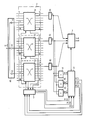
- the switching matrix 2 consists of three individual, mutually identical, parallel ones Sub-switching networks 21, 22 and 23 each with m input lines and k output lines. For the sake of clarity, only one line of the m input lines leading to this switching matrix and of the k output lines leading away from this switching matrix and the circuit arrangements lying in these lines is shown in the drawing with the circuit arrangements lying in these two lines.
- the signal path between an nth input nE via switching matrix 2 and an lth output lX is shown.
- Each of the input lines E leading to the switching matrix is divided into three sub-switching fields by a distributor, which is designed m-fold according to the number of input lines.
- the nth input line is fed to the distributor 10, for example.
- Each distributor consists of three decoupling stages - the distributor 10, for example, the decoupling stages 11, 12 and 13 - the inputs of which are connected to one another.
- Each output of a decoupling stage is connected to an input of a sub-switching network, the order of the connections of the sub-switching networks being chosen to be the same.
- nth input nE is connected to the nth distributor 10 and the output of the first decoupling component 11 of this nth distributor 10 is connected to the nth input of the first sub-switching matrix 21, and the output of the second decoupling component 12 is connected to the
- the n-th input of the second sub-switching network 22 and the output of the third decoupling module 23 are connected to the n-th input of the third sub-switching network 23.
- the setting data for the partial switching networks are calculated by a setting computer 3 and all partial switching networks fed at the same time. In this way, the same connection path is switched through in each sub-switching network for one and the same switching process. In a known manner, the setting computer 3 is executed several times in order to also carry out the connection setup in an error-protected manner.
- Each output of the sub-switching matrix is fed to a register in which the transmitted data is temporarily stored. With k output lines, k registers are provided three times. In this case, comparable outputs of the three sub-switching networks are combined in groups of three.
- the lth output of the first sub-switching matrix 21 is fed to a first register 41, the lth output of the second sub-switching matrix 22 to a second register 42 and the lth output of the third sub-switching matrix 23 to a third register 43.
- Data words A, B and C are present at the outputs of registers 41, 42, 43. As long as there are no signal falsifications on the signal path via the switching matrix, data words A, B and C have the same data content as each other, since they all originate from the same input data word.
- Each output of the register is connected on the one hand to a data input of a multiplexer 7 and on the other hand to the inputs of comparators 51, 52 and 53 which compare the data words A, B, C in pairs so that all possible combinations of two are checked.
- data words A and B are fed to the two inputs of first comparator 51, data words B and C to two inputs of second comparator 52, and data words A and C to the two inputs of third comparator 53. If the two data words to be compared match, the comparator in question delivers one at its output positive logic level.
- the outputs of these comparators 51, 52, 53 are fed to an evaluation logic 6 which controls a multiplexer 7. With the help of the multiplexer 7, one of the three data words A, B, C is selected as the output value.
- the comparators are executed three times k, multiplexer 7 and selection logic 6 times.
- the selection logic is constructed such that in this case the data word A is always selected using corresponding control information which is applied to the data selection input of the multiplexer 7.
- first data word A and the second data word B match, then A is again selected as the output word via the multiplexer 7 and an error signal F (3) which indicates an error in the third sub-switching network 23 is generated. If the second data word B and the third data word C match, then the second data word B is selected and an error signal F (1) for the first sub-switching matrix 21 generated; if, on the other hand, the first data word A and the third data word C match, then the first data word A is again selected and an error signal F (2) is generated for the second sub-switching network 22.
- a data word is always selected that has the highest probability of matching the input data word.
- All error signals assigned to a sub-switching matrix are combined in an OR circuit, not shown, to form an error signal, so that a defect in the affected sub-switching matrix is already indicated in the case of a corrupted data word.
- the error signal is used, for example, for an optical status display.
- the use of three sub-switching networks offers the advantage that if one sub-switching network fails, two data words still remain which can be compared with one another. In this way, the switching system can continue to be operated without problems in most cases, the remaining two switching networks being checked together for transmission errors. A partial switching matrix marked as defective can therefore be replaced while the switching system is in operation, without interfering with the course of the switching operation.
- the circuitry for the selection and error detection logic is very low and due to the simple Structure of the logic results in only insignificant signal delays in the evaluation logic.
- the operation of the switching system is not interrupted as described above.
- the logic level "high” is supplied to all inputs of the registers 51, 52, 53 via pull-up resistors, not shown. If one of the two remaining sub-switching networks becomes defective in such a way that it also constantly delivers high levels at one or more outputs, these two falsified output values would match and would be selected as correct values. If such an error occurs in all output data of a sub-switching matrix, then an error signal is not even generated.
- the selection logic 6 is therefore supplied with a presence signal P (1), P (2) or P (3) via three further inputs. This signal indicates whether the switching matrix assigned to each signal is ready for operation.
- this signal is generated by a switch which is switched on after a partial switching matrix has been inserted into the switching matrix and is switched off before a partial switching matrix is removed.
- the selection logic 6 is constructed in such a way that, in the case of a presence signal which is not present, the output data of the relevant switching matrix is not used to select the data which is considered correct for this switching matrix. In any case, an error signal is generated.
- the system can even be operated with only one partial switching matrix. Since the missing two sub-switching networks are not taken into account due to the lack of their assigned presence signal when selecting the correct data word. Although the registers concerned consistently consistently high level hold, only the output data of the sub-switching network remaining in the switching system are switched through.
- the presence signal is generated by a permanent self-test of elementary functions of the sub-switching matrix concerned. These functions include compliance with the operating voltage and the presence of the system clock.
- a corresponding monitoring device is arranged in each sub-switching matrix, which feeds the presence signal generated by it via a signal line to the relevant inputs of the evaluation circuits.
- this sub-switching network After inserting a sub-switching network, this sub-switching network initially still supplies incorrect data words because it does not have the setting information for the existing connections. Therefore, in a further embodiment of the invention, only the setting computer 3 receives the presence signals of the sub-switching networks.
- the computer controls an update routine with which all setting data are transmitted to the newly used sub-switching network via the existing switching channels. Since the computer continues to receive the error signals, it can monitor whether the newly installed sub-switching network is working properly. Only then is the corresponding presence signal passed on to the selection logic and only from this point in time on are the output data of the newly used sub-switching matrix used for the selection. In this way, high operational reliability of the entire switching system is achieved.
Landscapes
- Engineering & Computer Science (AREA)
- Computer Networks & Wireless Communication (AREA)
- Data Exchanges In Wide-Area Networks (AREA)
- Detection And Prevention Of Errors In Transmission (AREA)
Applications Claiming Priority (2)
| Application Number | Priority Date | Filing Date | Title |
|---|---|---|---|
| DE3801123 | 1988-01-16 | ||
| DE3801123A DE3801123A1 (de) | 1988-01-16 | 1988-01-16 | Vermittlungsanlage |
Publications (3)
| Publication Number | Publication Date |
|---|---|
| EP0325318A2 true EP0325318A2 (fr) | 1989-07-26 |
| EP0325318A3 EP0325318A3 (en) | 1990-11-14 |
| EP0325318B1 EP0325318B1 (fr) | 1994-08-17 |
Family
ID=6345401
Family Applications (1)
| Application Number | Title | Priority Date | Filing Date |
|---|---|---|---|
| EP89200057A Expired - Lifetime EP0325318B1 (fr) | 1988-01-16 | 1989-01-11 | Central de commutation |
Country Status (4)
| Country | Link |
|---|---|
| US (1) | US4995042A (fr) |
| EP (1) | EP0325318B1 (fr) |
| JP (1) | JP2849819B2 (fr) |
| DE (2) | DE3801123A1 (fr) |
Cited By (9)
| Publication number | Priority date | Publication date | Assignee | Title |
|---|---|---|---|---|
| EP0371570A3 (fr) * | 1988-11-01 | 1991-01-30 | Dsc Communications Corporation | Dispositif de commutation de remplacement |
| EP0466224A1 (fr) * | 1990-07-10 | 1992-01-15 | Telefonaktiebolaget L M Ericsson | Procédé et dispositif pour surveiller et vérifier un vote majoritaire |
| EP0535396A1 (fr) * | 1991-09-30 | 1993-04-07 | Siemens Aktiengesellschaft | Procédé pour la réduction de fautes de bit dans un système de communication digital |
| EP0517442A3 (fr) * | 1991-06-05 | 1994-03-02 | American Telephone & Telegraph | |
| DE4232955A1 (de) * | 1992-10-01 | 1994-04-07 | Philips Patentverwaltung | Vermittlungssystem |
| EP0582848A3 (fr) * | 1992-08-11 | 1995-06-21 | Siemens Ag | Procédé de détection d'erreurs dans des systèmes de communication numériques. |
| EP0665701A1 (fr) * | 1994-01-26 | 1995-08-02 | Siemens Aktiengesellschaft | Procédé pour la surveillance des chemins de connexion dans un central de commutation numérique à division dans le temps |
| WO1997020436A3 (fr) * | 1995-11-29 | 1997-07-31 | Ericsson Telefon Ab L M | Procede et appareil pour la verification de la connexion entre elements de circuits |
| WO1999045688A3 (fr) * | 1998-03-06 | 1999-10-21 | Nokia Telecommunications Oy | Systeme de commutation redondant |
Families Citing this family (6)
| Publication number | Priority date | Publication date | Assignee | Title |
|---|---|---|---|---|
| GB8921082D0 (en) * | 1989-09-18 | 1989-11-01 | Plessey Telecomm | Message routing check system |
| DE4228361C1 (de) * | 1992-08-26 | 1994-04-14 | Siemens Nixdorf Inf Syst | Digitales Koppelnetzwerk |
| ES2173079T3 (es) * | 1992-11-20 | 2002-10-16 | Siemens Ag | Procedimiento para la supervision de conexiones telefonicas existentes, especialmente conexiones telefonicas conmutadas de forma permanente. |
| DE4326919A1 (de) * | 1993-08-11 | 1995-02-16 | Teves Gmbh Alfred | Regelschaltung für Bremsanlagen mit ABS und/oder ASR |
| KR100301575B1 (ko) * | 1995-12-22 | 2001-11-22 | 박종섭 | 신호 전송장치 |
| US5903574A (en) * | 1997-04-18 | 1999-05-11 | Sarnoff Corporation | Studio transmitter link method and apparatus |
Family Cites Families (15)
| Publication number | Priority date | Publication date | Assignee | Title |
|---|---|---|---|---|
| US3431557A (en) * | 1964-03-12 | 1969-03-04 | Bendix Corp | Monitoring system for redundant systems |
| US3770948A (en) * | 1972-05-26 | 1973-11-06 | Gte Automatic Electric Lab Inc | Data handling system maintenance arrangement |
| JPS5419128B2 (fr) * | 1974-06-21 | 1979-07-12 | ||
| JPS5155643A (ja) * | 1974-11-11 | 1976-05-15 | Omron Tateisi Electronics Co | Denshikeisankiseigyohoshiki |
| DE2718317A1 (de) * | 1977-04-25 | 1978-11-02 | Gen Electric Co Ltd | Digital koppelnde fernmeldevermittlungseinrichtung |
| US4233682A (en) * | 1978-06-15 | 1980-11-11 | Sperry Corporation | Fault detection and isolation system |
| US4271515A (en) * | 1979-03-23 | 1981-06-02 | John Fluke Mfg. Co., Inc. | Universal analog and digital tester |
| DE2936439C2 (de) * | 1979-09-08 | 1983-02-17 | Wabco Westinghouse Fahrzeugbremsen GmbH, 3000 Hannover | Anordnung zur asynchronen Übertragung von digitalen Radgeschwindigkeits-Meßwerten |
| DE3003291C2 (de) * | 1980-01-30 | 1983-02-24 | Siemens AG, 1000 Berlin und 8000 München | Zweikanalige Datenverarbeitungsanordnung für Eisenbahnsicherungszwecke |
| JPS5736356A (en) * | 1980-08-12 | 1982-02-27 | Nippon Signal Co Ltd:The | Mutiplexing system |
| JPS5857843A (ja) * | 1981-09-30 | 1983-04-06 | Fujitsu Ltd | デ−タ回線交換装置のチエツク方式 |
| DE3336747C2 (de) * | 1983-10-08 | 1985-11-28 | Deutsche Thomson-Brandt Gmbh, 7730 Villingen-Schwenningen | Verfahren zur Auswertung eines aus mehreren Codeelementen bestehenden Steuercodewortes |
| JPS6182201A (ja) * | 1984-09-29 | 1986-04-25 | Nec Home Electronics Ltd | フエイルセ−フ制御回路 |
| DE3537451A1 (de) * | 1985-10-22 | 1987-04-23 | Philips Patentverwaltung | Vermittlungsanlage mit fehlerkorrektur |
| US4817094A (en) * | 1986-12-31 | 1989-03-28 | International Business Machines Corporation | Fault tolerant switch with selectable operating modes |
-
1988
- 1988-01-16 DE DE3801123A patent/DE3801123A1/de not_active Withdrawn
-
1989
- 1989-01-09 US US07/296,269 patent/US4995042A/en not_active Expired - Fee Related
- 1989-01-11 EP EP89200057A patent/EP0325318B1/fr not_active Expired - Lifetime
- 1989-01-11 DE DE58908195T patent/DE58908195D1/de not_active Expired - Fee Related
- 1989-01-13 JP JP505189A patent/JP2849819B2/ja not_active Expired - Lifetime
Cited By (14)
| Publication number | Priority date | Publication date | Assignee | Title |
|---|---|---|---|---|
| EP0371570A3 (fr) * | 1988-11-01 | 1991-01-30 | Dsc Communications Corporation | Dispositif de commutation de remplacement |
| AU653739B2 (en) * | 1990-07-10 | 1994-10-13 | Telefonaktiebolaget Lm Ericsson (Publ) | A method and a device for supervising and testing majority voting |
| EP0466224A1 (fr) * | 1990-07-10 | 1992-01-15 | Telefonaktiebolaget L M Ericsson | Procédé et dispositif pour surveiller et vérifier un vote majoritaire |
| WO1992001357A1 (fr) * | 1990-07-10 | 1992-01-23 | Telefonaktiebolaget Lm Ericsson | Procede et dispositif de surveillance et de controle d'un vote majoritaire |
| EP0517442A3 (fr) * | 1991-06-05 | 1994-03-02 | American Telephone & Telegraph | |
| EP0535396A1 (fr) * | 1991-09-30 | 1993-04-07 | Siemens Aktiengesellschaft | Procédé pour la réduction de fautes de bit dans un système de communication digital |
| US5436915A (en) * | 1991-09-30 | 1995-07-25 | Siemens Aktiengesellschaft | Bit error reduction by using checksums in a switching network implemented as triplets |
| EP0582848A3 (fr) * | 1992-08-11 | 1995-06-21 | Siemens Ag | Procédé de détection d'erreurs dans des systèmes de communication numériques. |
| DE4232955A1 (de) * | 1992-10-01 | 1994-04-07 | Philips Patentverwaltung | Vermittlungssystem |
| EP0665701A1 (fr) * | 1994-01-26 | 1995-08-02 | Siemens Aktiengesellschaft | Procédé pour la surveillance des chemins de connexion dans un central de commutation numérique à division dans le temps |
| WO1997020436A3 (fr) * | 1995-11-29 | 1997-07-31 | Ericsson Telefon Ab L M | Procede et appareil pour la verification de la connexion entre elements de circuits |
| US5937032A (en) * | 1995-11-29 | 1999-08-10 | Telefonaktiebolaget L M | Testing method and apparatus for verifying correct connection of curcuit elements |
| WO1999045688A3 (fr) * | 1998-03-06 | 1999-10-21 | Nokia Telecommunications Oy | Systeme de commutation redondant |
| US6226261B1 (en) | 1998-03-06 | 2001-05-01 | Nokia Networks Oy | Redundant switching arrangement |
Also Published As
| Publication number | Publication date |
|---|---|
| EP0325318B1 (fr) | 1994-08-17 |
| EP0325318A3 (en) | 1990-11-14 |
| JP2849819B2 (ja) | 1999-01-27 |
| US4995042A (en) | 1991-02-19 |
| DE58908195D1 (de) | 1994-09-22 |
| JPH025657A (ja) | 1990-01-10 |
| DE3801123A1 (de) | 1989-07-27 |
Similar Documents
| Publication | Publication Date | Title |
|---|---|---|
| EP0325318B1 (fr) | Central de commutation | |
| DE3111447C2 (fr) | ||
| EP0219917B1 (fr) | Dispositif de commutation avec correction de fautes | |
| DE2053836C3 (de) | Anordnung zur Korrektur von Fehlerbündeln in binär codierten Datengruppen | |
| EP0127118B1 (fr) | Dispositif de commande de mémoire en particulier pour un système de central téléphonique tolérant des fautes | |
| DE69534316T2 (de) | Telekommunikationsanlage mit einem prozessorsystem und ein prozessorsystem | |
| DE68919963T2 (de) | Schutz gegen Verlust oder Verfälschung von Daten während der Umschaltung eines redundanten Systems. | |
| EP0182134A2 (fr) | Méthode de mise en oeuvre d'un système multicalculateurs à sécurité intrinsèque comportant plusieur circuits inprimés d'entrées/sorties à sécurité non intrinsèque | |
| DE3843564A1 (de) | Verfahren zur ueberpruefung von verbindungs- und/oder schalteinrichtungen und/oder -leitungen | |
| DE4300025C1 (de) | Verfahren und Einrichtung zur fehlercodierenden Datenübertragung | |
| DE69011590T2 (de) | Verfahren und Vorrichtung zur Detektierung und Ortung von Fehlern in einer mehretagigen Einheit eines digitalen Zeitumschaltungsmoduls. | |
| EP0094902A2 (fr) | Procédé pour localiser des sources d'erreur dans des systèmes numériques et brouilleur/débrouilleur pour la réalisation de ce procédé | |
| EP0263563B1 (fr) | Central à multiplexage temporel | |
| DE3010803C2 (de) | Schalteinrichtung für ein Dreirechner-System in Eisenbahnanlagen | |
| EP0029216A1 (fr) | Dispositif pour la transmission de données avec une mémoire-tampon et dispositifs pour la protection des données | |
| DE3821871A1 (de) | Breitbandkoppeleinrichtung | |
| EP0294678B1 (fr) | Dispositif de sécurité pour protéger les données dans des unités de mémoire d'un ordinateur par l'utilisation de codes de détection et correction d'erreurs | |
| EP0162270B1 (fr) | Méthode pour tester des chemins commutés d'un réseau de connexion multiplex à division dans l'espace | |
| DE3010803C3 (fr) | ||
| DE2504006A1 (de) | Verfahren zur gesicherten datenuebertragung parallel binaer codierter daten | |
| DE3315269C2 (de) | Schaltungsanordnung zur Erhöhung der Betriebssicherheit beim Informationsaustausch zwischen Steuereinrichtungen von Fernmelde-, insbesondere Fernsprechvermittlungsanlagen | |
| EP0665701A1 (fr) | Procédé pour la surveillance des chemins de connexion dans un central de commutation numérique à division dans le temps | |
| EP0029215B1 (fr) | Dispositif pour la transmission de données avec une mémoire-tampon et dispositifs pour la protection des données | |
| DE2025916B2 (de) | Dekodiernetzwerk mit fehlersicherung und fehleranzeige | |
| DE2831960C2 (de) | Sicherungseinrichtung für die empfangsseitige Auswerteschaltung einer Datenübertragungsanlage mit sich paarweise ausschließenden Informationen |
Legal Events
| Date | Code | Title | Description |
|---|---|---|---|
| PUAI | Public reference made under article 153(3) epc to a published international application that has entered the european phase |
Free format text: ORIGINAL CODE: 0009012 |
|
| AK | Designated contracting states |
Kind code of ref document: A2 Designated state(s): DE FR GB |
|
| PUAL | Search report despatched |
Free format text: ORIGINAL CODE: 0009013 |
|
| AK | Designated contracting states |
Kind code of ref document: A3 Designated state(s): DE FR GB |
|
| RHK1 | Main classification (correction) |
Ipc: H04Q 11/04 |
|
| 17P | Request for examination filed |
Effective date: 19910513 |
|
| 17Q | First examination report despatched |
Effective date: 19931118 |
|
| GRAA | (expected) grant |
Free format text: ORIGINAL CODE: 0009210 |
|
| AK | Designated contracting states |
Kind code of ref document: B1 Designated state(s): DE FR GB |
|
| REF | Corresponds to: |
Ref document number: 58908195 Country of ref document: DE Date of ref document: 19940922 |
|
| GBT | Gb: translation of ep patent filed (gb section 77(6)(a)/1977) |
Effective date: 19941110 |
|
| ET | Fr: translation filed | ||
| REG | Reference to a national code |
Ref country code: FR Ref legal event code: CD |
|
| PLBE | No opposition filed within time limit |
Free format text: ORIGINAL CODE: 0009261 |
|
| STAA | Information on the status of an ep patent application or granted ep patent |
Free format text: STATUS: NO OPPOSITION FILED WITHIN TIME LIMIT |
|
| 26N | No opposition filed | ||
| REG | Reference to a national code |
Ref country code: FR Ref legal event code: CD |
|
| REG | Reference to a national code |
Ref country code: GB Ref legal event code: IF02 |
|
| PGFP | Annual fee paid to national office [announced via postgrant information from national office to epo] |
Ref country code: FR Payment date: 20020125 Year of fee payment: 14 |
|
| PGFP | Annual fee paid to national office [announced via postgrant information from national office to epo] |
Ref country code: GB Payment date: 20020131 Year of fee payment: 14 |
|
| PGFP | Annual fee paid to national office [announced via postgrant information from national office to epo] |
Ref country code: DE Payment date: 20020320 Year of fee payment: 14 |
|
| PG25 | Lapsed in a contracting state [announced via postgrant information from national office to epo] |
Ref country code: GB Free format text: LAPSE BECAUSE OF NON-PAYMENT OF DUE FEES Effective date: 20030111 |
|
| PG25 | Lapsed in a contracting state [announced via postgrant information from national office to epo] |
Ref country code: DE Free format text: LAPSE BECAUSE OF NON-PAYMENT OF DUE FEES Effective date: 20030801 |
|
| GBPC | Gb: european patent ceased through non-payment of renewal fee | ||
| PG25 | Lapsed in a contracting state [announced via postgrant information from national office to epo] |
Ref country code: FR Free format text: LAPSE BECAUSE OF NON-PAYMENT OF DUE FEES Effective date: 20030930 |
|
| REG | Reference to a national code |
Ref country code: FR Ref legal event code: ST |